4-2017
Fachzeitschrift für Hochfrequenz- und Mikrowellentechnik
Fachzeitschrift für Hochfrequenz- und Mikrowellentechnik

Erfolgreiche ePaper selbst erstellen
Machen Sie aus Ihren PDF Publikationen ein blätterbares Flipbook mit unserer einzigartigen Google optimierten e-Paper Software.
RF & Wireless<br />
<br />
<br />
<br />
done by first doing a resonance scan with<br />
an unpowered system to determine the location,<br />
frequency and Q of a resonant circuits<br />
(The amount of coupling enhancement due<br />
to resonance depends on the Q of the circuit.).<br />
Since one cannot reasonably test<br />
every point at every frequency for sensitivity,<br />
it’s reasonable to test only the identified<br />
locations and frequencies which will<br />
significantly reduce test time.<br />
When the engineer can determine what resonances<br />
exist in a design – location, frequency<br />
and Q – steps can be taken to minimize the<br />
potential for RF Immunity problems.<br />
Once the RF immunity scan at resonant locations<br />
is complete, the engineer will have a<br />
complete set of information: location, frequency,<br />
Q and the relative sensitivity at<br />
each location and therefore the likelihood<br />
that any resonant location will be a problem.<br />
Scanning and Shield<br />
Effectiveness Evaluation<br />
Using an automated scanning system with<br />
field measurement software and specialized<br />
probes can provide very accurate shielding<br />
effectiveness measurements to 18 GHz.<br />
With the correct probes, some as small as<br />
.025 mm or even 0.1 mm, it’s possible to<br />
achieve enough spatial resolution to accurately<br />
measure the shielding effectiveness<br />
of small DUTs and IC’s. Software can provide<br />
full test reports to minimize the engineers<br />
time evaluating the results.<br />
Current Spreading<br />
Current Spreading is a method of using an<br />
EMC Scanner to visually re-constructing<br />
the current flow on a board caused by a<br />
transient event.<br />
Using a well-controlled current sources and<br />
specially designed probes, it is possible to<br />
make measurements over an entire DUT and<br />
produce a video that shows how the injected<br />
currents flow with a resolution of better<br />
than 100 ps. This can be extremely useful<br />
to determine the performance of protection<br />
components and aide in determining where<br />
protective devices may need to be located.<br />
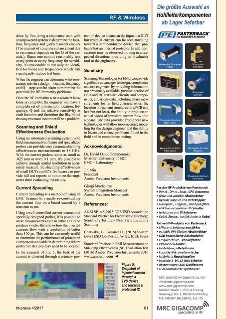
In the example of Fig. 5, the bulk of the<br />
current is diverted through a primary protection<br />
device located at the input to a DUT<br />
but residual current can be seen traveling<br />
toward a semiconductor device that probably<br />
has an internal protector. In addition,<br />
currents may be observed moving in unexpected<br />
directions providing an invaluable<br />
tool to the engineers.<br />
Summary<br />
Scanning Technologies for EMC can provide<br />
significant advantages to design, compliance<br />
and test engineers by providing information<br />
not previously available: precise location of<br />
ESD and RF sensitive circuits and components,<br />
emissions data including phase measurements<br />
for far field characteristics, the<br />
location of resonant structures on a PCB and<br />
last but not least, the ability to produce an<br />
actual video of transient current flow into<br />
a board. The data provided from these new<br />
technologies will allow more accurate modeling<br />
for the design engineer and the ability<br />
to locate and correct problems found in the<br />
field and in compliance testing.<br />
Acknowledgments:<br />
Dr. David David Pommerenke<br />
Missouri University of S&T<br />
EMC – Laboratory<br />
Jin Min<br />
President<br />
Amber Precision Instruments<br />
Giorgi Muchaidze<br />
System Integration Manager<br />
Amber Precision Instruments<br />
References:<br />
ANSI SP14.5-2015 EOS/ESD Association<br />
Standard Practice for Electrostatic Discharge<br />
Sensitivity Testing – Near Field Immunity<br />
Scanning<br />
Charvaka, D., Gossner H., (2015) System<br />
Level ESD Co-Design, Wiley, IEEE Press<br />
Standard Practice in EMI Measurement on<br />
Shielding Effectiveness (SE) Evaluation Test<br />
(2016) Amber Precision Instruments 2016<br />
www.amberpi.com ◄<br />
Figure 5:<br />
Snapshot of<br />
injected current<br />
through a<br />
TVS device<br />
and towards a<br />
protected IC<br />
<br />
<br />
<br />
<br />
<br />
<br />
<br />
<br />
!<br />
<br />
<br />
<br />
<br />
<br />
<br />
<br />
!<br />
<br />
"#<br />
<br />
<br />
<br />
<br />
<br />
<br />
!"<br />
<br />
#<br />
! !!<br />
<br />
$%&$'<br />
#%( <br />
<br />
")* <br />
#%(<br />
"$' <br />
!+,!-<br />
!!"<br />
!+../<br />
,(#$<br />
0 !%$<br />
<br />
<br />
<br />
!"#$%&%'(!<br />
!)$#$&*'&+,<br />
-!,.'/$/'"0"%//'*#(1'%<br />
hf-praxis 4/<strong>2017</strong> 81