EF 2019-2020
Fachzeitschrift für Hochfrequenz- und Mikrowellentechnik
Fachzeitschrift für Hochfrequenz- und Mikrowellentechnik

Erfolgreiche ePaper selbst erstellen
Machen Sie aus Ihren PDF Publikationen ein blätterbares Flipbook mit unserer einzigartigen Google optimierten e-Paper Software.
RF & Wireless<br />
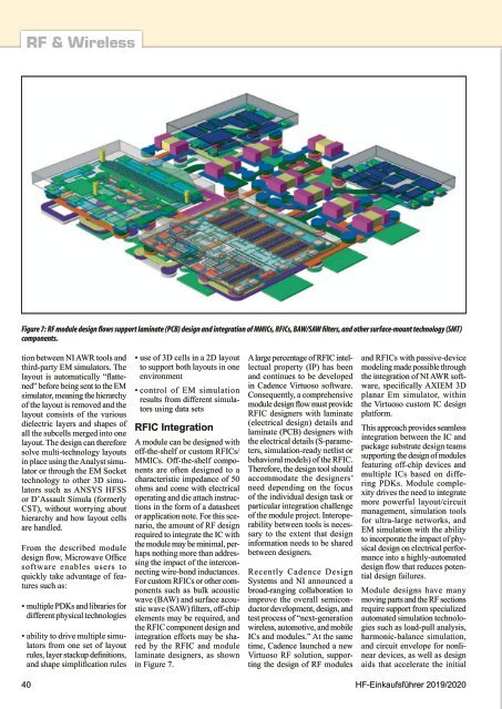
Figure 7: RF module design flows support laminate (PCB) design and integration of MMICs, RFICs, BAW/SAW filters, and other surface-mount technology (SMT)<br />
components.<br />
tion between NI AWR tools and<br />
third-party EM simulators. The<br />
layout is automatically “flattened”<br />
before being sent to the EM<br />
simulator, meaning the hierarchy<br />
of the layout is removed and the<br />
layout consists of the various<br />
dielectric layers and shapes of<br />
all the subcells merged into one<br />
layout. The design can therefore<br />
solve multi-technology layouts<br />
in place using the Analyst simulator<br />
or through the EM Socket<br />
technology to other 3D simulators<br />
such as ANSYS HFSS<br />
or D’Assault Simula (formerly<br />
CST), without worrying about<br />
hierarchy and how layout cells<br />
are handled.<br />
From the described module<br />
design flow, Microwave Office<br />
software enables users to<br />
quickly take advantage of features<br />
such as:<br />
• multiple PDKs and libraries for<br />
different physical technologies<br />
• ability to drive multiple simulators<br />
from one set of layout<br />
rules, layer stackup definitions,<br />
and shape simplification rules<br />
• use of 3D cells in a 2D layout<br />
to support both layouts in one<br />
environment<br />
• control of EM simulation<br />
results from different simulators<br />
using data sets<br />
RFIC Integration<br />
A module can be designed with<br />
off-the-shelf or custom RFICs/<br />
MMICs. Off-the-shelf components<br />
are often designed to a<br />
characteristic impedance of 50<br />
ohms and come with electrical<br />
operating and die attach instructions<br />
in the form of a datasheet<br />
or application note. For this scenario,<br />
the amount of RF design<br />
required to integrate the IC with<br />
the module may be minimal, perhaps<br />
nothing more than addressing<br />
the impact of the interconnecting<br />
wire-bond inductances.<br />
For custom RFICs or other components<br />
such as bulk acoustic<br />
wave (BAW) and surface acoustic<br />
wave (SAW) filters, off-chip<br />
elements may be required, and<br />
the RFIC component design and<br />
integration efforts may be shared<br />
by the RFIC and module<br />
laminate designers, as shown<br />
in Figure 7.<br />
A large percentage of RFIC intellectual<br />
property (IP) has been<br />
and continues to be developed<br />
in Cadence Virtuoso software.<br />
Consequently, a comprehensive<br />
module design flow must provide<br />
RFIC designers with laminate<br />
(electrical design) details and<br />
laminate (PCB) designers with<br />
the electrical details (S-parameters,<br />
simulation-ready netlist or<br />
behavioral models) of the RFIC.<br />
Therefore, the design tool should<br />
accommodate the designers’<br />
need depending on the focus<br />
of the individual design task or<br />
particular integration challenge<br />
of the module project. Interoperability<br />
between tools is necessary<br />
to the extent that design<br />
information needs to be shared<br />
between designers.<br />
Recently Cadence Design<br />
Systems and NI announced a<br />
broad-ranging collaboration to<br />
improve the overall semiconductor<br />
development, design, and<br />
test process of “next-generation<br />
wireless, automotive, and mobile<br />
ICs and modules.” At the same<br />
time, Cadence launched a new<br />
Virtuoso RF solution, supporting<br />
the design of RF modules<br />
and RFICs with passive-device<br />
modeling made possible through<br />
the integration of NI AWR software,<br />
specifically AXIEM 3D<br />
planar Em simulator, within<br />
the Virtuoso custom IC design<br />
platform.<br />
This approach provides seamless<br />
integration between the IC and<br />
package substrate design teams<br />
supporting the design of modules<br />
featuring off-chip devices and<br />
multiple ICs based on differing<br />
PDKs. Module complexity<br />
drives the need to integrate<br />
more powerful layout/circuit<br />
management, simulation tools<br />
for ultra-large networks, and<br />
EM simulation with the ability<br />
to incorporate the impact of physical<br />
design on electrical performance<br />
into a highly-automated<br />
design flow that reduces potential<br />
design failures.<br />
Module designs have many<br />
moving parts and the RF sections<br />
require support from specialized<br />
automated simulation technologies<br />
such as load-pull analysis,<br />
harmonic-balance simulation,<br />
and circuit envelope for nonlinear<br />
devices, as well as design<br />
aids that accelerate the initial<br />
40 HF-Einkaufsführer <strong>2019</strong>/<strong>2020</strong>