EF 2019-2020
Fachzeitschrift für Hochfrequenz- und Mikrowellentechnik
Fachzeitschrift für Hochfrequenz- und Mikrowellentechnik

Sie wollen auch ein ePaper? Erhöhen Sie die Reichweite Ihrer Titel.
YUMPU macht aus Druck-PDFs automatisch weboptimierte ePaper, die Google liebt.
RF & Wireless<br />
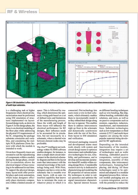
Figure 4: EM simulation is often required to electrically characterize passive components and interconnects such as transitions between layers<br />
of multi-layer substrates.<br />
is a challenging task at higher<br />
frequencies where electrical characterization<br />
must be performed<br />
using EM simulation of structures<br />
implemented via layoutfocused<br />
design tools, as shown in<br />
Figure 4. In this design phase, the<br />
focus is on electrical modeling of<br />
the floor plan while addressing<br />
the physical I/O requirements of<br />
the IC, integrating the package<br />
substrate constraints and variables,<br />
and considering the multiple<br />
PCB platforms (form factors)<br />
with which the module is<br />
intended to work.<br />
Given how frequently traces are<br />
rerouted to suit the repositioning<br />
of components within a module<br />
during the design phase, circuit/<br />
EM co-simulation allows the<br />
electrical impact of trace rerouting<br />
to be addressed in real time.<br />
To support the physical design,<br />
many layout tools offer powerful<br />
place-and-route automation,<br />
which helps designers efficiently<br />
place electronic components<br />
within a limited amount of<br />
space. This is followed by routing,<br />
which determines the optimum<br />
wiring path based on a set<br />
of defined rules and limitations<br />
of the manufacturing process.<br />
Since the width and length of<br />
these traces will influence the<br />
electrical performance for RF<br />
designs, their influence needs<br />
to be accounted for in simulation,<br />
but not necessarily in a<br />
schematic, where a shorted wire<br />
between element nodes may be<br />
preferable.<br />
The iNet intelligent net technology<br />
within NI AWR software<br />
enables designer, for instance, to<br />
draw a simple short-circuit interconnect<br />
in the electrical schematic<br />
diagram and then in the layout<br />
route that interconnect with the<br />
internal knowledge of the technology<br />
being used. With iNets,<br />
designers can have a wire on the<br />
schematic that is routable over<br />
many layers, with an auto via<br />
insertion capability that knows<br />
how to terminate the route on<br />
whatever pin(s) to which it is<br />
connected. iNet technology lets<br />
users route a wire in their schematic,<br />
which ultimately enables<br />
them to incrementally model it<br />
as they refined their design along<br />
the way to tapeout. This enables<br />
them to address interconnects<br />
right up front in the schematic<br />
and dynamically synchronize<br />
them with the rest of the flow,<br />
from layout to EM simulation<br />
and verification.<br />
Advanced packaging research<br />
and development teams must<br />
work closely with system and<br />
circuit design teams to optimize<br />
interconnect and embedded passive<br />
technologies for size, reliability,<br />
and performance, and to<br />
develop and incorporate parametric-based<br />
RF models within existing<br />
design flows. Considerable<br />
research activity is dedicated to<br />
characterizing and modeling the<br />
RF properties of various assembly<br />
techniques in order to reduce<br />
parasitics and optimize the<br />
signal transmission characteristics.<br />
Special interest focuses<br />
on different bonding techniques<br />
such as wire bonding, flip chip,<br />
ribbon bonding, embedded chip<br />
solutions, and more, as well as<br />
on-passive components such as<br />
resistors, capacitors, inductors,<br />
transformers, and transmission<br />
lines. Substrate technologies<br />
such as low-temperature co-fired<br />
ceramic (LTCC) and multi-layer<br />
organics are among the more<br />
popular materials being developed<br />
for RF applications.<br />
Depending on the intended<br />
functionality of the module,<br />
integration may require a set<br />
of technologies such as wafer<br />
thinning, embedded passive<br />
components, vertical system<br />
integration, assembly of thin<br />
components, thin interconnect<br />
technologies, bumping/ball<br />
placing, and dicing. All these<br />
technologies need to be optimized<br />
and adapted in a modular<br />
integrated process flow. Advanced<br />
module packaging acts as<br />
a system-integration carrier,<br />
with the potential to reduce the<br />
38 HF-Einkaufsführer <strong>2019</strong>/<strong>2020</strong>