shot noise in mesoscopic conductors - Low Temperature Laboratory
shot noise in mesoscopic conductors - Low Temperature Laboratory
shot noise in mesoscopic conductors - Low Temperature Laboratory

Create successful ePaper yourself
Turn your PDF publications into a flip-book with our unique Google optimized e-Paper software.
86 Ya.M. Blanter, M. Bu( ttiker / Physics Reports 336 (2000) 1}166<br />
4. Shot <strong>noise</strong> <strong>in</strong> hybrid normal and superconduct<strong>in</strong>g structures<br />
The dissipationless current (supercurrent) <strong>in</strong> super<strong>conductors</strong> is a property of a ground state, and<br />
therefore is <strong>noise</strong>less } it is not accompanied by any #uctuations. However, <strong>noise</strong> appears if the<br />
superconductor is <strong>in</strong> contact with piece(s) of normal metals. This section is devoted to the<br />
description of <strong>shot</strong> <strong>noise</strong> <strong>in</strong> these hybrid structures, which exhibit a variety of <strong>in</strong>terest<strong>in</strong>g phenomena.<br />
Follow<strong>in</strong>g the po<strong>in</strong>t of view of the previous sections, we present here a description which<br />
is based on an extension of the scatter<strong>in</strong>g approach to hybrid structures.<br />
4.1. Shot <strong>noise</strong> of normal-superconductor <strong>in</strong>terfaces<br />
4.1.1. Simple NS <strong>in</strong>terface, scatter<strong>in</strong>g theory and general expressions<br />
We consider "rst an <strong>in</strong>terface of normal metal and superconductor (NS). If the applied voltage is<br />
below the superconduct<strong>in</strong>g gap , the only mechanism of charge transport is Andreev re#ection at<br />
the NS <strong>in</strong>terface: an electron with energy E approach<strong>in</strong>g the <strong>in</strong>terface from the normal side is<br />
converted <strong>in</strong>to a hole with energy !E. The velocity of the hole is directed back from the <strong>in</strong>terface<br />
to a normal metal. The miss<strong>in</strong>g charge 2e on the normal side appears as a new Cooper pair on the<br />
superconduct<strong>in</strong>g side. There is, of course, also a reverse process, when a Cooper pair recomb<strong>in</strong>es<br />
with a hole <strong>in</strong> the normal conductor, and creates an electron. At equilibrium, both processes have<br />
the same probability, and there is thus no net current. However, if a voltage is applied, a "nite<br />
current #ows across the NS <strong>in</strong>terface.<br />
The scatter<strong>in</strong>g theory which we described <strong>in</strong> Section 2 has to be extended to take <strong>in</strong>to account<br />
the Andreev scatter<strong>in</strong>g processes [167]. We give here only a sketch of the derivation; a more<br />
detailed description, as well as a comprehensive list of references, may be found <strong>in</strong> Refs. [72,168].<br />
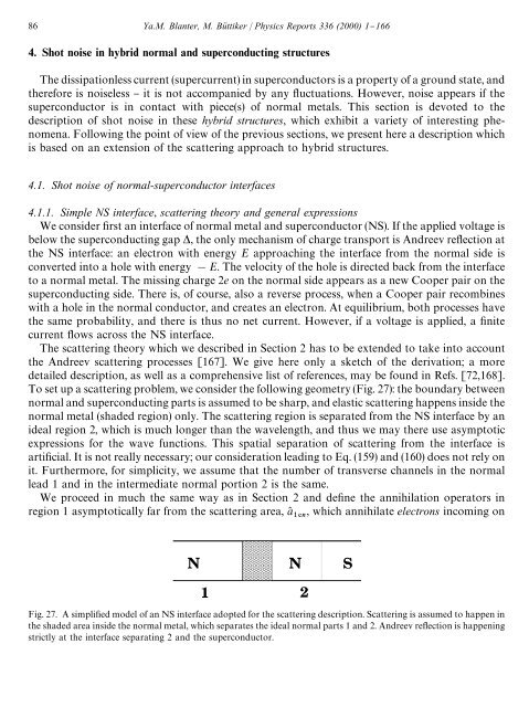
To set up a scatter<strong>in</strong>g problem, we consider the follow<strong>in</strong>g geometry (Fig. 27): the boundary between<br />
normal and superconduct<strong>in</strong>g parts is assumed to be sharp, and elastic scatter<strong>in</strong>g happens <strong>in</strong>side the<br />
normal metal (shaded region) only. The scatter<strong>in</strong>g region is separated from the NS <strong>in</strong>terface by an<br />
ideal region 2, which is much longer than the wavelength, and thus we may there use asymptotic<br />
expressions for the wave functions. This spatial separation of scatter<strong>in</strong>g from the <strong>in</strong>terface is<br />
arti"cial. It is not really necessary; our consideration lead<strong>in</strong>g to Eq. (159) and (160) does not rely on<br />
it. Furthermore, for simplicity, we assume that the number of transverse channels <strong>in</strong> the normal<br />
lead 1 and <strong>in</strong> the <strong>in</strong>termediate normal portion 2 is the same.<br />
We proceed <strong>in</strong> much the same way as <strong>in</strong> Section 2 and de"ne the annihilation operators <strong>in</strong><br />
region 1 asymptotically far from the scatter<strong>in</strong>g area, a( , which annihilate electrons <strong>in</strong>com<strong>in</strong>g on<br />
Fig. 27. A simpli"ed model of an NS <strong>in</strong>terface adopted for the scatter<strong>in</strong>g description. Scatter<strong>in</strong>g is assumed to happen <strong>in</strong><br />
the shaded area <strong>in</strong>side the normal metal, which separates the ideal normal parts 1 and 2. Andreev re#ection is happen<strong>in</strong>g<br />
strictly at the <strong>in</strong>terface separat<strong>in</strong>g 2 and the superconductor.