Photonics Driving Economic Growth in Europe - Photonics21
Photonics Driving Economic Growth in Europe - Photonics21
Photonics Driving Economic Growth in Europe - Photonics21

Create successful ePaper yourself
Turn your PDF publications into a flip-book with our unique Google optimized e-Paper software.
2. <strong>Photonics</strong> Research and Innovation Challenges<br />
photonics, III-V semiconductors and dielectric and<br />
polymer materials. Furthermore, just as <strong>in</strong> microelectronics,<br />
we must <strong>in</strong>vest significant scientific<br />
resources <strong>in</strong> the development and evolution of<br />
robust, accurate and efficient simulation and computer<br />
aided design (CAD) tools and <strong>in</strong> process and<br />
packag<strong>in</strong>g technologies support<strong>in</strong>g the generic<br />
platform approach. Consideration should also be<br />
given to the <strong>in</strong>tegration of optical circuit design<br />
tools with systems-level simulation tools, <strong>in</strong> order<br />
to facilitate a holistic approach to the development<br />
of application-specific products based on<br />
PIC technology.<br />
In order to expedite the future evolution of our<br />
chosen platforms, we propose research on largescale<br />
<strong>in</strong>tegration processes allow<strong>in</strong>g the seamless<br />
<strong>in</strong>troduction of new technologies. It is vital that<br />
the platforms can embrace new technologies with<br />
potential for improvements <strong>in</strong> functionality, compactness,<br />
energy efficiency, manufacturability or<br />
cost-effectiveness. Technologies such as photonic<br />
circuits based on membranes, nanowires, photonic<br />
crystals, metamaterials and plasmonics, <strong>in</strong>clud<strong>in</strong>g<br />
optical antenna structures, should be supported,<br />
and opportunities sought to <strong>in</strong>tegrate these ele-<br />
ments <strong>in</strong>to generic PIC capabilities at the earliest<br />
opportunity. In addition, extension to new wavelength<br />
ranges (for example, visible, UV) should<br />
be addressed. Further advances <strong>in</strong> manufactur<strong>in</strong>g<br />
techniques will certa<strong>in</strong>ly also be required, for example,<br />
developments <strong>in</strong> high-volume, high precision,<br />
and cost-effective techniques, such as nanoimpr<strong>in</strong>t<br />
lithography (NIL).<br />
Alongside the development of device and circuit<br />
technology, a concerted attack must be made on<br />
the challenges of cost-effective manufactur<strong>in</strong>g<br />
of components and subsystems. Here we need<br />
to deploy <strong>Europe</strong>an expertise on robotics, automated<br />
precision assembly and test technologies<br />
to offset the cost advantage of Far-Eastern manufacturers,<br />
and ensure that the full value cha<strong>in</strong> can<br />
be addressed with<strong>in</strong> <strong>Europe</strong>. We envisage here a<br />
synergistic exploitation of electronic, optical and<br />
mechanical technologies <strong>in</strong> an optimum comb<strong>in</strong>ation.<br />
New structures with improved capacity for<br />
heat dissipation and thermal control are essential,<br />
as are strategies for manag<strong>in</strong>g electromagnetic<br />
design challenges. <strong>Europe</strong>an strengths <strong>in</strong> hybrid<br />
photonic <strong>in</strong>tegration, <strong>in</strong>clud<strong>in</strong>g photonic lightwave<br />
circuit technologies, should be exploited, along<br />
<strong>Europe</strong>an strengths <strong>in</strong><br />
hybrid photonic <strong>in</strong>tegration,<br />
73<br />
<strong>in</strong>clud<strong>in</strong>g photonic lightwave<br />
circuit technologies, are<br />
a major advantage.<br />
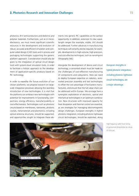
High frequency wafer level test<strong>in</strong>g<br />
of germanium photodiodes on silicon.<br />
© CEA-Leti