Photonics Driving Economic Growth in Europe - Photonics21
Photonics Driving Economic Growth in Europe - Photonics21
Photonics Driving Economic Growth in Europe - Photonics21

Create successful ePaper yourself
Turn your PDF publications into a flip-book with our unique Google optimized e-Paper software.
74 Towards 2020 – <strong>Photonics</strong> driv<strong>in</strong>g economic growth <strong>in</strong> <strong>Europe</strong><br />
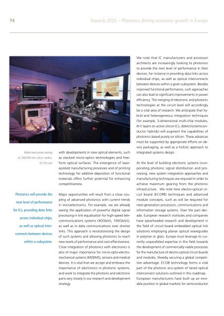
Wafer-level probe test<strong>in</strong>g<br />
on 200/300 mm silicon wafers.<br />
© CEA-Leti<br />
<strong>Photonics</strong> will provide the<br />
next level of performance<br />
for ICs, provid<strong>in</strong>g data l<strong>in</strong>ks<br />
across <strong>in</strong>dividual chips,<br />
as well as optical <strong>in</strong>ter-<br />
connects between devices<br />
with<strong>in</strong> a subsystem.<br />
with developments <strong>in</strong> new optical elements, such<br />
as stacked micro-optics technologies and free-<br />
form optical surfaces. The emergence of laser-<br />
assisted manufactur<strong>in</strong>g processes and of pr<strong>in</strong>t<strong>in</strong>g<br />
technology for additive deposition of functional<br />
materials offers further potential for enhanc<strong>in</strong>g<br />
competitiveness.<br />
Major opportunities will result from a close coupl<strong>in</strong>g<br />
of advanced photonics with current trends<br />
<strong>in</strong> microelectronics. For example, we are already<br />
see<strong>in</strong>g the application of powerful digital signal<br />
process<strong>in</strong>g <strong>in</strong> l<strong>in</strong>k equalisation for high-speed telecommunications<br />
systems (40Gbit/s, 100Gbit/s),<br />
as well as <strong>in</strong> data communications over shorter<br />
l<strong>in</strong>ks. This approach is revolutionis<strong>in</strong>g the design<br />
of such systems and allow<strong>in</strong>g photonics to reach<br />
new levels of performance and cost-effectiveness.<br />
Close <strong>in</strong>tegration of photonics with electronics is<br />
also of major importance for micro-opto-electromechanical<br />
systems (MOEMS), sensors and medical<br />
devices. It is vital that we accept and embrace the<br />
importance of electronics <strong>in</strong> photonic systems,<br />
and work to <strong>in</strong>tegrate the photonic and electronic<br />
parts very closely <strong>in</strong> our research and development<br />
strategy.<br />
We note that IC manufacturers and processor<br />
architects are <strong>in</strong>creas<strong>in</strong>gly look<strong>in</strong>g to photonics<br />
to provide the next level of performance <strong>in</strong> their<br />
devices, for <strong>in</strong>stance <strong>in</strong> provid<strong>in</strong>g data l<strong>in</strong>ks across<br />
<strong>in</strong>dividual chips, as well as optical <strong>in</strong>terconnects<br />
between devices with<strong>in</strong> a given subsystem. Besides<br />
improved functional performance, such approaches<br />
can also lead to significant improvements <strong>in</strong> power<br />
efficiency. The merg<strong>in</strong>g of electronic and photonic<br />
technologies at the circuit level will accord<strong>in</strong>gly<br />
be a vital area of research. We anticipate that hybrid<br />
and heterogeneous <strong>in</strong>tegration techniques<br />
(for example, 3-dimensional multi-chip modules,<br />
III-V layers on active silicon ICs, dielectric/semiconductor<br />
hybrids) will augment the capabilities of<br />
photonics based purely on silicon. These advances<br />
must be supported by appropriate efforts on device<br />
packag<strong>in</strong>g, as well as a holistic approach to<br />
<strong>in</strong>tegrated systems design.<br />
At the level of build<strong>in</strong>g electronic systems <strong>in</strong>corporat<strong>in</strong>g<br />
photonic signal distribution and process<strong>in</strong>g,<br />
new system <strong>in</strong>tegration approaches and<br />
manu factur<strong>in</strong>g techniques are required <strong>in</strong> order to<br />
achieve maximum gear<strong>in</strong>g from the photonic<br />
<strong>in</strong>fra structure. We note here electro-optical circuit<br />
board (ECOPB) techniques and advanced<br />
module concepts, such as will be required for<br />
next-generation processors, communications and<br />
<strong>in</strong>formation storage systems. Over the past decade,<br />
<strong>Europe</strong>an research <strong>in</strong>stitutes and companies<br />
have spear headed research and development <strong>in</strong><br />
the field of circuit board embedded optical l<strong>in</strong>k<br />
solutions employ<strong>in</strong>g planar optical waveguides<br />
<strong>in</strong> polymer or glass. <strong>Europe</strong> must leverage its currently<br />
unparalleled expertise <strong>in</strong> this field towards<br />
the development of commercially viable processes<br />
for the manufacture of electro-optical circuit boards<br />
and modules, thereby secur<strong>in</strong>g a global competitive<br />
advantage. ECOB technology forms a vital<br />
part of the photonic eco-system of tiered optical<br />
<strong>in</strong>terconnect solutions outl<strong>in</strong>ed <strong>in</strong> this roadmap.<br />
<strong>Europe</strong>an manufacturers have built up an enviable<br />
position <strong>in</strong> global markets for semiconductor