

Demystifying Auto-Zero Amplifiers—Part 1 - Analog Devices
Demystifying Auto-Zero Amplifiers—Part 1 - Analog Devices
Demystifying Auto-Zero Amplifiers—Part 1 - Analog Devices

You also want an ePaper? Increase the reach of your titles
YUMPU automatically turns print PDFs into web optimized ePapers that Google loves.
<strong>Demystifying</strong> <strong>Auto</strong>-<strong>Zero</strong><br />
<strong>Amplifiers—Part</strong> 1<br />
They essentially eliminate offset, drift,<br />
and 1/f noise. How do they work?<br />
Is there a downside?<br />
by Eric Nolan<br />
INTRODUCTION<br />
Whenever the subject of auto-zero or chopper-stabilized amplifiers<br />
comes up, the inevitable first question is “How do they really work?”<br />
Beyond curiosity about the devices’ inner workings, the real<br />
question in most engineers’ minds is, perhaps, “The dc precision<br />
looks incredible, but what kind of weird behavior am I going to<br />
have to live with if I use one of these in my circuit; and how can I<br />
design around the problems?” Part 1 of this article will attempt to<br />
answer both questions. In Part 2, to appear in the next issue, some<br />
very popular and timely applications will be mentioned to illustrate<br />
the significant advantages, as well as some of the drawbacks, of<br />
these parts.<br />
Chopper Amplifiers—How They Work<br />
The first chopper amplifiers were invented more than 50 years<br />
ago to combat the drift of dc amplifiers by converting the dc voltage<br />
to an ac signal. Initial implementations used switched ac coupling<br />
of the input signal and synchronous demodulation of the ac signal<br />
to re-establish the dc signal at the output. These amplifiers had<br />
limited bandwidth and required post-filtering to remove the large<br />
ripple voltages generated by the chopping action.<br />
Chopper-stabilized amplifiers solved the bandwidth limitations by<br />
using the chopper amplifier to stabilize a conventional wide-band<br />
amplifier that remained in the signal path * . Early chopper-stabilized<br />
designs were only capable of inverting operation, since the<br />
stabilizing amplifier’s output was connected directly to the noninverting<br />
input of the wide-band differential amplifier. Modern<br />
IC “chopper” amplifiers actually employ an auto-zero approach<br />
using a two-or-more-stage composite amplifier structure similar<br />
to the chopper-stabilized scheme. The difference is that the<br />
stabilizing amplifier signals are connected to the wide-band or main<br />
amplifier through an additional “nulling” input terminal, rather<br />
than one of the differential inputs. Higher-frequency signals bypass<br />
the nulling stage by direct connection to the main amplifier or<br />
through the use of feed-forward techniques, maintaining a stable<br />
zero in wide-bandwidth operation.<br />
This technique thus combines dc stability and good frequency<br />
response with the accessibility of both inverting and noninverting<br />
configurations. However, it may produce interfering signals<br />
consisting of high levels of digital switching “noise” that limit the<br />
usefulness of the wider available bandwidth. It also causes<br />
intermodulation distortion (IMD), which looks like aliasing between<br />
the clock signal and the input signal, producing error signals at<br />
the sum and difference frequencies. More about that later.<br />
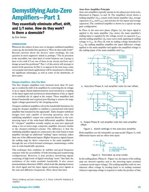
<strong>Auto</strong>-<strong>Zero</strong> Amplifier Principle<br />
<strong>Auto</strong>-zero amplifiers typically operate in two phases per clock cycle,<br />
illustrated in Figures 1a and 1b. The simplified circuit shows a<br />
nulling amplifier (A A ), a main (wide-band) amplifier (A B ), storage<br />
capacitors (C M1 and C M2 ), and switches for the inputs and storage<br />
capacitors. The combined amplifier is shown in a typical op-amp<br />
gain configuration.<br />
In Phase A, the auto-zero phase (Figure 1a), the input signal is<br />
applied to the main amplifier (A B ) alone; the main amplifier’s<br />
nulling input is supplied by the voltage stored on capacitor C M2 ;<br />
and the nulling amplifier (A A ) auto-zeros itself, applying its nulling<br />
voltage to C M1 . In Phase B, with its nulling voltage furnished by<br />
C M1 , the nulling amplifier amplifies the input difference voltage<br />
applied to the main amplifier and applies the amplified voltage to<br />
the nulling input of the main amplifier and C M2 .<br />
V I+<br />
V I–<br />
B<br />
A<br />
V OSB<br />
A B<br />
V NB<br />
EXTERNAL<br />
FEEDBACK<br />
V OSA<br />
A A<br />
V NA A B<br />
C M1 C M2<br />
V O<br />
a. <strong>Auto</strong>-<strong>Zero</strong> Phase A: null amplifier nulls its own offset.<br />
V I+<br />
V I–<br />
B<br />
A<br />
V OSB<br />
A B<br />
V NB<br />
EXTERNAL<br />
FEEDBACK<br />
V OSA<br />
A A<br />
V NA A B<br />
C M1 C M2<br />
V O<br />
b. Output Phase B: null amplifier nulls the main amplifier<br />
offset.<br />
Figure 1. Switch settings in the auto-zero amplifier.<br />
Both amplifiers use the trimmable op-amp model (Figure 2), with<br />
differential inputs and an offset-trim input.<br />
V<br />
V<br />
V I+<br />
A<br />
V I–<br />
B<br />
N<br />
O<br />
V O = A(V I+ –V I– ) +BV N<br />
A = DIFFERENTIAL GAIN<br />
B = TRIM GAIN<br />
Figure 2. Trimmable op amp model.<br />
In the nulling phase (Phase A—Figure 1a), the inputs of the nulling<br />
amp are shorted together and to the inverting input terminal<br />
(common-mode input voltage). The nulling amplifier nulls its own<br />
inherent offset voltage by feeding back to its nulling terminal<br />
whatever opposing voltage is required to make the product of that<br />
*<br />
Edwin Goldberg and Jules Lehmann, U. S. Patent 2,684,999: Stabilized dc<br />
amplifier.<br />
<strong>Analog</strong> Dialogue 34-2 (2000) 25


