

Demystifying Auto-Zero Amplifiers—Part 1 - Analog Devices
Demystifying Auto-Zero Amplifiers—Part 1 - Analog Devices
Demystifying Auto-Zero Amplifiers—Part 1 - Analog Devices

Create successful ePaper yourself
Turn your PDF publications into a flip-book with our unique Google optimized e-Paper software.
Selecting an <strong>Analog</strong><br />
Front-End for Imaging<br />
Applications<br />
by Kevin Buckley<br />
INTRODUCTION<br />
Every imaging system starts with an image sensor. The signal from<br />
the sensor must be processed in the analog domain, converted to<br />
digital, and further processed in the digital domain. This allows<br />
the image to be analyzed, manipulated, and enhanced, prior to<br />
storage, display, transmission, and/or further processing. Imaging<br />
applications typically involve three chips—an image sensor, an<br />
analog front-end (AFE), and a digital ASIC. The AFE conditions<br />
the analog signal received from the image sensor and performs<br />
the analog-to-digital (A/D) conversion. The digital ASIC contains<br />
image-processing and timing-generation circuitry. Figure 1 shows<br />
a block diagram of a typical imaging system. Additional<br />
application-specific circuitry following the digital imageprocessing<br />
ASIC depends upon whether the imaging system is a<br />
camera, scanner or copier.<br />
OPTICS<br />
IMAGE<br />
SENSOR<br />
RAW<br />
ANALOG<br />
IMAGE<br />
ANALOG<br />
FRONT<br />
END<br />
RAW<br />
DIGITAL<br />
IMAGE<br />
IMAGE<br />
PROCESSING<br />
UNIT<br />
TIMING<br />
GENERATION<br />
PROCESSED<br />
DIGITAL<br />
IMAGE<br />
Figure 1. Block diagram of a typical imaging application.<br />
<strong>Analog</strong> front-ends. A typical AFE starts with an input clamp.<br />
The common-mode level of the image sensor’s output signal could<br />
range from 0 V to more than 9 V, so the signal must be ac-coupled<br />
to the AFE. The input clamp restores the dc level of the signal to<br />
an optimum point within the supply range of the AFE.<br />
A sampling function follows the input clamp. AFEs designed to<br />
work with charge-coupled devices (CCDs) use a correlated double<br />
sampler (CDS). The CDS takes two samples of each pixel, one at<br />
the reset level and one at the video level, and performs a differential<br />
measurement between the two. The CDS improves the signal-tonoise<br />
ratio (SNR) by eliminating the correlated kT/C noise<br />
associated with the output stage of the CCD, and by attenuating<br />
low frequency drift. Contact image-sensors (CIS) and focal-plane<br />
arrays (FPA) used in commercial infrared (IR)-imaging<br />
applications typically output a single-ended, ground-referenced<br />
signal, and do not require a differential measurement. AFEs<br />
designed to work with these sensors use a sample-hold amplifier<br />
(SHA) in place of the CDS. A coarse black-level offset-correction<br />
stage is integrated with the CDS or SHA.<br />
A programmable- (or variable-) gain amplifier (PGA or VGA)<br />
follows the CDS to amplify the signal and better utilize the full<br />
dynamic range of the A/D converter (ADC). If black-level offset<br />
correction is not performed ahead of the PGA, the dynamic range<br />
of the imaging system will suffer. A high-speed ADC converts the<br />
conditioned analog image signal to the digital domain, allowing<br />
for additional processing by a digital ASIC.<br />
The AFE is programmed via a standard serial port that easily<br />
interfaces with most off-the-shelf microcontrollers or the digital<br />
ASIC. The PGA-gain registers, offset-correction registers, and<br />
sampling modes are all programmed through this interface.<br />
The choice of an AFE for an imaging application depends on many<br />
factors, including: the type of sensor being used, dynamic range,<br />
resolution, speed, noise, and power requirements. This article is<br />
intended to provide a guide to making appropriate AFE choices<br />
for imaging applications.<br />
DIGITAL VIDEO AND STILL CAMERA APPLICATIONS<br />
Digital video and still cameras are among the fastest-growing<br />
segments in consumer electronics today. Camera manufacturers<br />
continually need to create higher-performance cameras at lower<br />
cost in order to remain competitive. This need has driven IC<br />
manufacturers to higher levels of circuit integration in order to<br />
reduce the size and cost of camera components.<br />
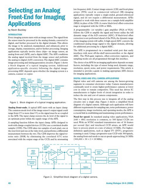
The first step in this process was to integrate all of the analog<br />
circuitry into a single chip. Figure 2 shows a simplified block<br />
diagram of a digital camera. Although each application will have<br />
different requirements for sampling rate, noise performance, power<br />
consumption, image resolution, and operating modes, the AFE is<br />
a crucial link in establishing and maintaining system performance.<br />
Need for speed. In standard analog video applications, VGA<br />
(640 × 480) resolution is common, so 300 kpixel CCDs are<br />
used. With an NTSC-standard transmission rate of 30 frames<br />
per second (fps) and interlaced CCD arrays, an AFE would<br />
have to process pixels at a rate of almost 10 MHz. For higherdefinition<br />
applications, such as digital TV (DTV), progressive<br />
scanning is used. Using a progressive-scan CCD with 300 kpixels,<br />
the analog front-end needs to run at speeds approaching 20 MHz<br />
(300,000 × 30 × 2 = 18 MHz).<br />
AREA<br />
CCD<br />
ARRAY<br />
ANALOG<br />
FRONT<br />
END<br />
+<br />
CDS<br />
VGA<br />
ADC<br />
10/12<br />
IMAGE<br />
PROCESSING<br />
UNIT<br />
VIDEO<br />
DAC<br />
LCD<br />
DISPLAY<br />
VERTICAL<br />
DRIVE<br />
DC BIAS<br />
CLP<br />
COMPRESSION<br />
HOST<br />
INTERFACE<br />
TIMING<br />
GENERATION<br />
Figure 2. Simplified block diagram of a digital camera.<br />
40 <strong>Analog</strong> Dialogue 34-6 (2000)


