Full Custom IC Desig..
Full Custom IC Desig..
Full Custom IC Desig..

You also want an ePaper? Increase the reach of your titles
YUMPU automatically turns print PDFs into web optimized ePapers that Google loves.
Introduction<br />
This manual assumes you are able to do some basic things in a Linux environment such as create<br />
a folder, change directories....etc. If you want to learn how to use Linux here are many good<br />
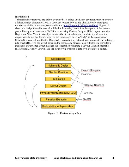
tutorials available on the web, such as this one: http://tldp.org/LDP/gs/node5.html. Figure I.1<br />
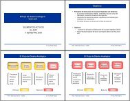
shows the design flow this tutorial will be implementing. In the first three parts of this manual<br />
you will design and simulate a CMOS inverter using <strong>Custom</strong> <strong>Desig</strong>nerSE in conjunction with<br />
Hspice and WaveView to visually assemble the circuit schematic, simulate it, and view the<br />
output waveforms. For further help you are encouraged to go to “Help” in the menu bar of<br />
CosmosSE. You will use Custon <strong>Desig</strong>nerSE to create a layout, and use Hercules to run a design<br />
rule check (DRC) on the layout based on the technology process. You will also use Hercules to<br />
make sure our inverter layout matches our schematic by running a Layout Versus Schematic<br />
(LVS) check. Finally, you will use the inverter we create in a gate level design of a buffer.<br />
Figure I.1: <strong>Custom</strong> design flow<br />
San Francisco State University Nano‐electronics and Computing Research Lab 3