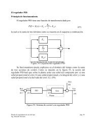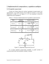
Full Custom IC Desig..
Full Custom IC Desig..
Full Custom IC Desig..

Create successful ePaper yourself
Turn your PDF publications into a flip-book with our unique Google optimized e-Paper software.
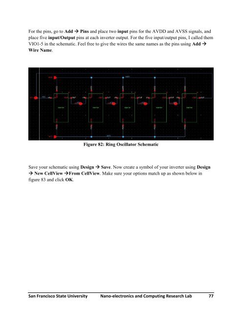
For the pins, go to Add Pins and place two input pins for the AVDD and AVSS signals, and<br />
place five input/Output pins at each inverter output. For the five input/output pins, I called them<br />
VIO1-5 in the schematic. Feel free to give the wires the same names as the pins using Add <br />
Wire Name.<br />
Figure 82: Ring Oscillator Schematic<br />
Save your schematic using <strong>Desig</strong>n Save. Now create a symbol of your inverter using <strong>Desig</strong>n<br />
New CellView From CellView. Make sure your options match up as shown below in<br />
figure 83 and click OK.<br />
San Francisco State University Nano‐electronics and Computing Research Lab 77