

Application Note AN-1035 - International Rectifier
Application Note AN-1035 - International Rectifier
Application Note AN-1035 - International Rectifier

You also want an ePaper? Increase the reach of your titles
YUMPU automatically turns print PDFs into web optimized ePapers that Google loves.
Design considerations<br />
Substrates<br />
DirectFET technology was originally developed and<br />
evaluated for use with epoxy and polyimide glasswoven<br />
substrates. The test substrates were finished in<br />
electroless nickel immersion gold but any of the<br />
numerous surface finishes available are suitable.<br />
Subsequent evaluations have confirmed that<br />
DirectFET devices can be used with insulated metal<br />
substrates made from aluminum silicon carbide<br />
(AlSiC) and copper (Cu). For more information, refer<br />
to the DirectFET Technology Materials and Practices<br />
<strong>Application</strong> <strong>Note</strong> (<strong>AN</strong>-1050), available at:<br />
www.irf.com/technical-info/appnotes/an-1050.pdf<br />
The substrate finish can affect the amount of energy<br />
required to make solder joints; this can in turn be a<br />
factor in solder quality issues such as solder balling,<br />
tombstoning (or tilt) and the formation of voids. It is<br />
important to ensure that the appropriate reflow profile<br />
is used for the selected substrate finish.<br />
Substrate designs<br />
To achieve low-loss track layouts, DirectFET devices<br />
were designed for use with solder-mask-defined<br />
layouts. Although the devices can be used with paddefined<br />
(non-solder-mask-defined) layouts, these have<br />
not been evaluated. The outline of DirectFET devices<br />
and the use of solder-mask-defined pads contribute to<br />
efficient substrate design. Large-area tracks optimize<br />
electrical and thermal performance.<br />
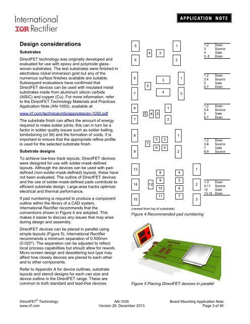
If pad numbering is required to produce a component<br />
outline within the library of a CAD system,<br />
<strong>International</strong> <strong>Rectifier</strong> recommends that the<br />
conventions shown in Figure 4 are adopted. This<br />
makes it easier to discuss any issues that may arise<br />
during design and assembly.<br />
DirectFET devices can be placed in parallel using<br />
simple layouts (Figure 5). <strong>International</strong> <strong>Rectifier</strong><br />
recommends a minimum separation of 0.500mm<br />
(0.020"). The separation can be adjusted to reflect<br />
local process capabilities but should allow for rework.<br />
Micro-screen design and desoldering tool type may<br />
affect how closely devices are placed to each other<br />
and to other components.<br />
Refer to Appendix A for device outlines, substrate<br />
layouts and stencil designs for each can size and<br />
device outline in the DirectFET range. These are<br />
common to both standard and lead-free devices.<br />
5<br />
6<br />
6<br />
7<br />
6<br />
7<br />
5<br />
4<br />
8<br />
1<br />
5 3<br />
7<br />
6 4<br />
9 2<br />
13<br />
3<br />
8<br />
9 5<br />
14 12<br />
2<br />
10 6<br />
15<br />
5<br />
4 3<br />
3<br />
4<br />
1<br />
2<br />
1<br />
2<br />
4<br />
11 7<br />
(viewed from top of substrate)<br />
Figure 4 Recommended pad numbering<br />
Figure 5 Placing DirectFET devices in parallel<br />
1<br />
2<br />
1<br />
3<br />
1,2 Drain<br />
3 Source<br />
4 Gate<br />
5, 6 Drain<br />
1,2 Drain<br />
3,4 Source<br />
5 Gate<br />
6,7 Drain<br />
1,2 Drain<br />
3,4 Source<br />
5 Gate<br />
6,7 Drain<br />
1,2 Drain<br />
3-6 Source<br />
7 Gate<br />
8,9 Source<br />
1-3 Drain<br />
4-11 Source<br />
12 Gate<br />
13-15 Drain<br />
DirectFET ® Technology <strong>AN</strong>-<strong>1035</strong> Board Mounting <strong>Application</strong> <strong>Note</strong><br />
www.irf.com Version 26, December 2013 Page 3 of 40


