

Application Note AN-1035 - International Rectifier
Application Note AN-1035 - International Rectifier
Application Note AN-1035 - International Rectifier

Create successful ePaper yourself
Turn your PDF publications into a flip-book with our unique Google optimized e-Paper software.
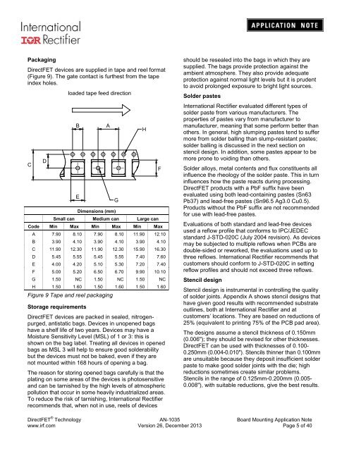
Packaging<br />
DirectFET devices are supplied in tape and reel format<br />
(Figure 9). The gate contact is furthest from the tape<br />
index holes.<br />
C<br />
D<br />
loaded tape feed direction<br />
B<br />
E<br />
Dimensions (mm)<br />
Small can Medium can Large can<br />
Code Min Max Min Max Min Max<br />
A 7.90 8.10 7.90 8.10 11.90 12.10<br />
B 3.90 4.10 3.90 4.10 3.90 4.10<br />
C 11.90 12.30 11.90 12.30 15.90 16.30<br />
D 5.45 5.55 5.45 5.55 7.40 7.60<br />
E 4.00 4.20 5.10 5.30 7.20 7.40<br />
F 5.00 5.20 6.50 6.70 9.90 10.10<br />
G 1.50 NC 1.50 NC 1.50 NC<br />
H 1.50 1.60 1.50 1.60 1.50 1.60<br />
Figure 9 Tape and reel packaging<br />
Storage requirements<br />
DirectFET devices are packed in sealed, nitrogenpurged,<br />
antistatic bags. Devices in unopened bags<br />
have a shelf life of two years. Devices may have a<br />
Moisture Sensitivity Level (MSL) of 1 or 3: this is<br />
shown on the bag label. Treating all devices in opened<br />
bags as MSL 3 will help to ensure good solderability<br />
but the devices must not be baked, even if they are<br />
not mounted within 168 hours of opening a bag.<br />
The reason for storing opened bags carefully is that the<br />
plating on some areas of the devices is photosensitive<br />
and can be tarnished by the high levels of atmospheric<br />
pollution that occur in some heavily industrialized areas.<br />
To reduce the risk of tarnishing, <strong>International</strong> <strong>Rectifier</strong><br />
recommends that, when not in use, reels of devices<br />
A<br />
G<br />
H<br />
F<br />
should be resealed into the bags in which they are<br />
supplied. The bags provide protection against the<br />
ambient atmosphere. They also provide adequate<br />
protection against normal light levels but it is prudent<br />
to avoid prolonged exposure to bright light sources.<br />
Solder pastes<br />
<strong>International</strong> <strong>Rectifier</strong> evaluated different types of<br />
solder paste from various manufacturers. The<br />
properties of pastes vary from manufacturer to<br />
manufacturer, meaning that some perform better than<br />
others. In general, high slumping pastes tend to suffer<br />
more from solder balling than slump-resistant pastes;<br />
solder balling is discussed in the next section on<br />
stencil design. In addition, some pastes appear to be<br />
more prone to voiding than others.<br />
Solder alloys, metal contents and flux constituents all<br />
influence the rheology of the solder paste. This in turn<br />
influences how the paste reacts during processing.<br />
DirectFET products with a PbF suffix have been<br />
evaluated using both lead-containing pastes (Sn63<br />
Pb37) and lead-free pastes (Sn96.5 Ag3.0 Cu0.5).<br />
Products without the PbF suffix are not recommended<br />
for use with lead-free pastes.<br />
Evaluations of both standard and lead-free devices<br />
used a reflow profile that conforms to IPC/JEDEC<br />
standard J-STD-020C (July 2004 revision). As devices<br />
may be subjected to multiple reflows when PCBs are<br />
double-sided or reworked, the evaluations used up to<br />
three reflows. <strong>International</strong> <strong>Rectifier</strong> recommends that<br />
customers should conform to J-STD-020C in setting<br />
reflow profiles and should not exceed three reflows.<br />
Stencil design<br />
Stencil design is instrumental in controlling the quality<br />
of solder joints. Appendix A shows stencil designs that<br />
have given good results with recommended substrate<br />
outlines, both at <strong>International</strong> <strong>Rectifier</strong> and at<br />
customers’ locations. They are based on reductions of<br />
25% (equivalent to printing 75% of the PCB pad area).<br />
The designs assume a stencil thickness of 0.150mm<br />
(0.006"); they should be revised for other thicknesses.<br />
DirectFET can be used with thicknesses of 0.100-<br />
0.250mm (0.004-0.010"). Stencils thinner than 0.100mm<br />
are unsuitable because they deposit insufficient solder<br />
paste to make good solder joints with the die; high<br />
reductions sometimes create similar problems.<br />
Stencils in the range of 0.125mm-0.200mm (0.005-<br />
0.008"), with suitable reductions, give the best results.<br />
DirectFET ® Technology <strong>AN</strong>-<strong>1035</strong> Board Mounting <strong>Application</strong> <strong>Note</strong><br />
www.irf.com Version 26, December 2013 Page 5 of 40


