

Application Note AN-1035 - International Rectifier
Application Note AN-1035 - International Rectifier
Application Note AN-1035 - International Rectifier

Create successful ePaper yourself
Turn your PDF publications into a flip-book with our unique Google optimized e-Paper software.
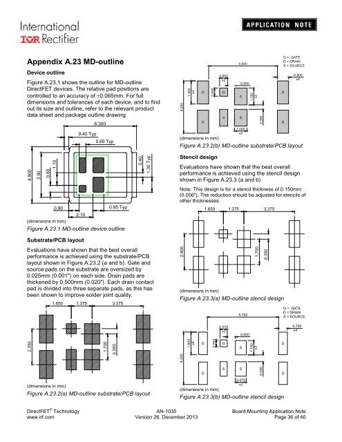
Appendix A.23 MD-outline<br />
Device outline<br />
Figure A.23.1 shows the outline for MD-outline<br />
DirectFET devices. The relative pad positions are<br />
controlled to an accuracy of ±0.065mm. For full<br />
dimensions and tolerances of each device, and to find<br />
out its size and outline, refer to the relevant product<br />
data sheet and package outline drawing<br />
6.300<br />
0.40 Typ<br />
0.60 Typ<br />
4.200<br />
1.850<br />
x4<br />
D<br />
D<br />
0.650<br />
0.650<br />
x2<br />
G<br />
S<br />
5.500<br />
0.550<br />
S<br />
S<br />
1.000<br />
x2<br />
1.350<br />
x3<br />
0.350<br />
G = GATE<br />
D = DRAIN<br />
S = SOURCE<br />
0.900<br />
x4<br />
(dimensions in mm)<br />
Figure A.23.2(b) MD-outline substrate/PCB layout<br />
D<br />
D<br />
4.900<br />
3.90<br />
0.60<br />
1.10<br />
0.40<br />
1.30 Typ<br />
Stencil design<br />
Evaluations have shown that the best overall<br />
performance is achieved using the stencil design<br />
shown in Figure A.23.3 (a and b)<br />
0.90<br />
0.95 Typ<br />
2.10<br />
(dimensions in mm)<br />
Figure A.23.1 MD-outline device outline<br />
<strong>Note</strong>: This design is for a stencil thickness of 0.150mm<br />
(0.006"). The reduction should be adjusted for stencils of<br />
other thicknesses.<br />
1.650 1.375 3.375<br />
Substrate/PCB layout<br />
Evaluations have shown that the best overall<br />
performance is achieved using the substrate/PCB<br />
layout shown in Figure A.23.2 (a and b). Gate and<br />
source pads on the substrate are oversized by<br />
0.025mm (0.001") on each side. Drain pads are<br />
thickened by 0.500mm (0.020"). Each drain contact<br />
pad is divided into three separate pads, as this has<br />
been shown to improve solder joint quality.<br />
1.650 1.375 3.375<br />
2.400<br />
1.700<br />
0.350<br />
(dimensions in mm)<br />
Figure A.23.3(a) MD-outline stencil design<br />
5.700<br />
G = GATE<br />
D = DRAIN<br />
S = SOURCE<br />
0.575<br />
x2<br />
0.650<br />
0.700<br />
x4<br />
2.350<br />
1.700<br />
0.350<br />
1.800<br />
x4<br />
D<br />
0.550<br />
G<br />
S<br />
1.150<br />
x3<br />
D<br />
4.200<br />
(dimensions in mm)<br />
Figure A.23.2(a) MD-outline substrate/PCB layout<br />
D<br />
S<br />
0.875<br />
x2<br />
(dimensions in mm)<br />
Figure A.23.3(b) MD-outline stencil design<br />
S<br />
0.550<br />
D<br />
DirectFET ® Technology <strong>AN</strong>-<strong>1035</strong> Board Mounting <strong>Application</strong> <strong>Note</strong><br />
www.irf.com Version 26, December 2013 Page 36 of 40


