

Application Note AN-1035 - International Rectifier
Application Note AN-1035 - International Rectifier
Application Note AN-1035 - International Rectifier

Create successful ePaper yourself
Turn your PDF publications into a flip-book with our unique Google optimized e-Paper software.
heatsink<br />
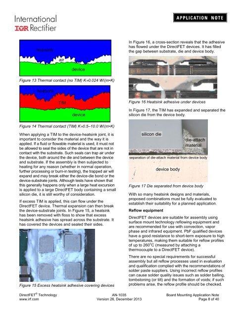
In Figure 16, a cross-section reveals that the adhesive<br />
has flowed under the DirectFET devices. It has filled<br />
the gap between substrate, die and device body.<br />
air<br />
device<br />
Figure 13 Thermal contact (no TIM) K≈0.024 W/(m•K)<br />
heatsink<br />
TIM<br />
device<br />
Figure 16 Heatsink adhesive under devices<br />
In Figure 17, the TIM has expanded and separated the<br />
silicon die from the device body.<br />
Figure 14 Thermal contact (TIM) K≈0.5–10.0 W/(m•K)<br />
When applying a TIM to the device-heatsink joint, it is<br />
important to consider the material and the way it is<br />
applied. If a fluid or flowable material is used, it must not<br />
be allowed to seal the sides of the device that are not in<br />
contact with the substrate. Such seals can trap air under<br />
the device, both around the die and between the device<br />
and substrate. If the assembly is then subjected to<br />
heating for any reason (whether in normal operation,<br />
further processing or burn-in testing), the trapped air will<br />
expand and may break either the device-die bond or the<br />
device-substrate joints. Although tests have shown that<br />
this generally happens only when a large heat excursion<br />
is applied to a large DirectFET body containing a small<br />
silicon die, it is still worthy of consideration.<br />
If excess TIM is applied, this can flow under the<br />
DirectFET device. Thermal expansion can then break<br />
the device-substrate joints. In Figure 15, a heatsink<br />
has been removed with floss to show that excess<br />
heatsink adhesive has spread across the substrate. It<br />
has covered the devices and sealed their sides.<br />
Figure 15 Excess heatsink adhesive covering devices<br />
silicon die<br />
die-attach<br />
material<br />
separation of die-attach material from device body<br />
device body<br />
Figure 17 Die separated from device body<br />
With so many heatsink designs and materials,<br />
proposed combinations must be fully evaluated to<br />
establish their suitability for a planned application.<br />
Reflow equipment<br />
DirectFET devices are suitable for assembly using<br />
surface mount technology reflowing equipment and<br />
are recommended for use with convection, vapor<br />
phase and infrared equipment. PbF qualified devices<br />
have a good resistance to short-term exposure to high<br />
temperatures, making them suitable for reflow profiles<br />
of up to 260 o C (measured by attaching a<br />
thermocouple to a DirectFET device).<br />
There are no special requirements for successful<br />
assembly but all reflow processes used in evaluation<br />
and qualification complied with the recommendations of<br />
solder paste suppliers. Using incorrect reflow profiles<br />
can cause solder quality issues such as solder balling,<br />
tombstoning (or tilt) and the formation of voids; if such<br />
problems arise, the reflow profile should be checked.<br />
DirectFET ® Technology <strong>AN</strong>-<strong>1035</strong> Board Mounting <strong>Application</strong> <strong>Note</strong><br />
www.irf.com Version 26, December 2013 Page 8 of 40


