

Application Note AN-1035 - International Rectifier
Application Note AN-1035 - International Rectifier
Application Note AN-1035 - International Rectifier

Create successful ePaper yourself
Turn your PDF publications into a flip-book with our unique Google optimized e-Paper software.
Post-reflow evaluations can help to assess how a stencil<br />
is performing within a given process. Two main problem<br />
areas can be addressed by improving stencil design:<br />
• Solder balling around the perimeter of the die.<br />
This can be caused by too much solder paste, in<br />
which case the stencil might need to be reduced by<br />
more than 25%. The reduction can be symmetrical<br />
but biasing it unevenly may help to prevent solder<br />
balling; the stencil designs in Appendix A have<br />
apertures moved further from the die edge for this<br />
reason. Solder balling can result from other external<br />
factors, such as the moisture content of the board<br />
and incorrect ramp rates or insufficient soak times<br />
in the reflow profile. Leadless devices like<br />
DirectFET can sometime accentuate existing<br />
deficiencies within a process.<br />
• Misshapen joints. If the joints are smaller or<br />
seem to be only partially made, this might suggest<br />
that there is insufficient solder to make the joint. If,<br />
however, the joints have what appear to be<br />
additional areas extending from their edges, they<br />
are usually the result of too much solder; this<br />
almost certainly the case if solder balls are also<br />
present. Insufficient solder can also cause voiding<br />
but this is more likely to arise from other factors,<br />
including surface finish, solder paste and substrate<br />
condition.<br />
Device placement<br />
Due to the recessed position of the die, DirectFET<br />
devices should ideally be depressed into the solder<br />
paste by at least 0.050mm (0.002") to ensure that the<br />
contact areas are in full contact with the paste.<br />
Placement machines operate on various principles,<br />
some based on over-travel and others on placement<br />
pressure. Good results have been achieved using<br />
over-travel of 0.050mm-0.100mm (0.002-0.004") and<br />
placement pressure of 150-250g.<br />
Insufficient placement pressure may result in poor<br />
solder joints or in devices being tilted and/or<br />
misaligned. Although it is better to avoid perceptible<br />
tilt, poor placement does not always cause reflow<br />
problems. Ideally, devices should be placed to an<br />
accuracy of 0.050mm on both X and Y axes but,<br />
during evaluations, devices centered themselves from<br />
placement inaccuracies of more than 0.200mm.<br />
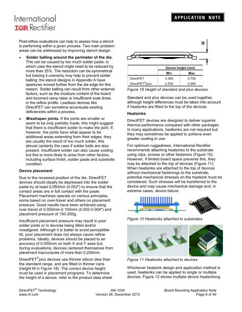
DirectFET ® plus devices use thinner silicon dies than<br />
the standard range, and are fitted in thinner cans<br />
(height M in Figure 18). The correct device height<br />
must be used in placement programs. To determine<br />
the height of a device, refer to the product data sheet.<br />
Device height (mm)<br />
Min<br />
Max<br />
DirectFET 0.590 0.700<br />
DirectFET ® plus 0.535 0.595<br />
Figure 18 Height of standard and plus devices<br />
Standard and plus devices can be used together,<br />
although height differences must be taken into account<br />
if heatsinks are fitted to the top of the devices.<br />
Heatsinks<br />
DirectFET devices are designed to deliver superior<br />
thermal performance compared with other packages.<br />
In many applications, heatsinks are not required but<br />
they may sometimes be applied to achieve even<br />
greater cooling in use.<br />
For optimum ruggedness, <strong>International</strong> <strong>Rectifier</strong><br />
recommends attaching heatsinks to the substrate<br />
using clips, screws or other fasteners (Figure 10).<br />
However, if limited board space prevents this, they<br />
may be attached to the top of devices (Figure 11).<br />
When heatsinks are attached to the top of devices<br />
without mechanical fastenings to the substrate,<br />
potential mechanical stresses on the heatsink must be<br />
considered. Such stresses will be transferred to the<br />
device and may cause mechanical damage and, in<br />
extreme cases, device failure.<br />
Figure 10 Heatsinks attached to substrates<br />
Figure 11 Heatsinks attached to devices<br />
Whichever heatsink design and application method is<br />
used, heatsinks can be applied to single or multiple<br />
devices. Figure 12 shows multiple device heatsinking.<br />
DirectFET ® Technology <strong>AN</strong>-<strong>1035</strong> Board Mounting <strong>Application</strong> <strong>Note</strong><br />
www.irf.com Version 26, December 2013 Page 6 of 40


