

Application Note AN-1035 - International Rectifier
Application Note AN-1035 - International Rectifier
Application Note AN-1035 - International Rectifier

Create successful ePaper yourself
Turn your PDF publications into a flip-book with our unique Google optimized e-Paper software.
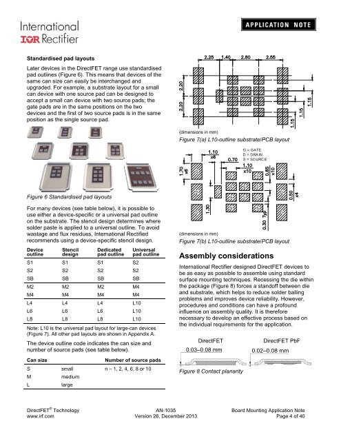
Standardised pad layouts<br />
Later devices in the DirectFET range use standardised<br />
pad outlines (Figure 6). This means that devices of the<br />
same can size can easily be interchanged and<br />
upgraded. For example, a substrate layout for a small<br />
can device with one source pad can be designed to<br />
accept a small can device with two source pads; the<br />
gate pads are in the same positions on the two<br />
devices and the first of two source pads is in the same<br />
position as the single source pad.<br />
(dimensions in mm)<br />
Figure 7(a) L10-outline substrate/PCB layout<br />
G = GATE<br />
D = DRA IN<br />
S = SOURC E<br />
D<br />
S<br />
S<br />
D<br />
Figure 6 Standardised pad layouts<br />
D<br />
G<br />
S<br />
S<br />
S<br />
S<br />
S<br />
S<br />
D<br />
For many devices (see table below), it is possible to<br />
use either a device-specific or a universal pad outline<br />
on the substrate. The stencil design determines where<br />
solder paste is applied to a universal outline. To avoid<br />
wastage and flux residues, <strong>International</strong> Rectified<br />
recommends using a device-specific stencil design.<br />
Device<br />
outline<br />
Stencil<br />
design<br />
Dedicated<br />
pad outline<br />
S1 S1 S1 S2<br />
S2 S2 S2 S2<br />
SB SB SB SB<br />
M2 M2 M2 M4<br />
M4 M4 M4 M4<br />
L4 L4 L4 L10<br />
L6 L6 L6 L10<br />
L8 L8 L8 L10<br />
Universal<br />
pad outline<br />
<strong>Note</strong>: L10 is the universal pad layout for large-can devices<br />
(Figure 7). All other pad layouts are shown in Appendix A.<br />
The device outline code indicates the can size and<br />
number of source pads (see table below).<br />
Can size<br />
Number of source pads<br />
S small n – 1, 2, 4, 6, 8 or 10<br />
M<br />
medium<br />
L<br />
large<br />
D<br />
S<br />
(dimensions in mm)<br />
Figure 7(b) L10-outline substrate/PCB layout<br />
Assembly considerations<br />
<strong>International</strong> <strong>Rectifier</strong> designed DirectFET devices to<br />
be as easy as possible to assemble using standard<br />
surface mounting techniques. Recessing the die within<br />
the package (Figure 8) forces a standoff between die<br />
and substrate, which helps to reduce solder balling<br />
problems and improves device reliability. However,<br />
procedures and conditions can have a profound<br />
influence on assembly quality. It is therefore<br />
necessary to develop an effective process based on<br />
the individual requirements for the application.<br />
DirectFET<br />
DirectFET PbF<br />
0.03–0.08 mm 0.02–0.08 mm<br />
Figure 8 Contact planarity<br />
S<br />
D<br />
DirectFET ® Technology <strong>AN</strong>-<strong>1035</strong> Board Mounting <strong>Application</strong> <strong>Note</strong><br />
www.irf.com Version 26, December 2013 Page 4 of 40


