SC16IS740/750/760 Single UART with I2C-bus/SPI interface, 64 ...
SC16IS740/750/760 Single UART with I2C-bus/SPI interface, 64 ...
SC16IS740/750/760 Single UART with I2C-bus/SPI interface, 64 ...

You also want an ePaper? Increase the reach of your titles
YUMPU automatically turns print PDFs into web optimized ePapers that Google loves.
NXP Semiconductors<br />
<strong>SC16IS740</strong>/<strong>750</strong>/<strong>760</strong><br />
<strong>Single</strong> <strong>UART</strong> <strong>with</strong> I 2 C-<strong>bus</strong>/<strong>SPI</strong> <strong>interface</strong>, <strong>64</strong>-byte FIFOs, IrDA SIR<br />
[1] FIFO reset requires at least two XTAL1 clocks, therefore, they cannot be reset <strong>with</strong>out the presence of the<br />
XTAL1 clock.<br />
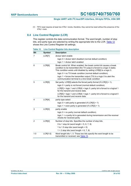
8.4 Line Control Register (LCR)<br />
This register controls the data communication format. The word length, number of stop<br />
bits, and parity type are selected by writing the appropriate bits to the LCR. Table 12<br />
shows the Line Control Register bit settings.<br />
Table 12. Line Control Register bits description<br />
Bit Symbol Description<br />
7 LCR[7] divisor latch enable<br />
logic 0 = divisor latch disabled (normal default condition)<br />
logic 1 = divisor latch enabled<br />
6 LCR[6] Break control bit. When enabled, the break control bit causes a break<br />
condition to be transmitted (the TX output is forced to a logic 0 state).<br />
This condition exists until disabled by setting LCR[6] to a logic 0.<br />
logic 0 = no TX break condition (normal default condition).<br />
logic 1 = forces the transmitter output (TX) to a logic 0 to alert the<br />
communication terminal to a line break condition<br />
5 LCR[5] Set parity. LCR[5] selects the forced parity format (if LCR[3] = 1).<br />
logic 0 = parity is not forced (normal default condition).<br />
LCR[5] = logic 1 and LCR[4] = logic 0: parity bit is forced to a logical 1<br />
for the transmit and receive data.<br />
LCR[5] = logic 1 and LCR[4] = logic 1: parity bit is forced to a logical 0<br />
for the transmit and receive data.<br />
4 LCR[4] parity type select<br />
logic 0 = odd parity is generated (if LCR[3] = 1)<br />
logic 1 = even parity is generated (if LCR[3] = 1)<br />
3 LCR[3] parity enable<br />
logic 0 = no parity (normal default condition).<br />
logic 1 = a parity bit is generated during transmission and the receiver<br />
checks for received parity<br />
2 LCR[2] Number of stop bits. Specifies the number of stop bits.<br />
0 to 1 stop bit (word length = 5, 6, 7, 8)<br />
1 to 1.5 stop bits (word length = 5)<br />
1 = 2 stop bits (word length = 6, 7, 8)<br />
1:0 LCR[1:0] Word length bits 1, 0. These two bits specify the word length to be<br />
transmitted or received; see Table 15.<br />
<strong>SC16IS740</strong>_<strong>750</strong>_<strong>760</strong>_6<br />
© NXP B.V. 2008. All rights reserved.<br />
Product data sheet Rev. 06 — 13 May 2008 24 of 62