SC16IS740/750/760 Single UART with I2C-bus/SPI interface, 64 ...
SC16IS740/750/760 Single UART with I2C-bus/SPI interface, 64 ...
SC16IS740/750/760 Single UART with I2C-bus/SPI interface, 64 ...

You also want an ePaper? Increase the reach of your titles
YUMPU automatically turns print PDFs into web optimized ePapers that Google loves.
NXP Semiconductors<br />
<strong>SC16IS740</strong>/<strong>750</strong>/<strong>760</strong><br />
<strong>Single</strong> <strong>UART</strong> <strong>with</strong> I 2 C-<strong>bus</strong>/<strong>SPI</strong> <strong>interface</strong>, <strong>64</strong>-byte FIFOs, IrDA SIR<br />
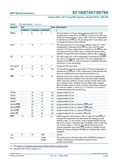
Table 2. Pin description …continued<br />
Symbol Pin Type Description<br />
TSSOP16 TSSOP24 HVQFN24<br />
CS/A0 2 9 6 I <strong>SPI</strong> chip select or I 2 C-<strong>bus</strong> device address select A0. If <strong>SPI</strong><br />
configuration is selected by <strong>I2C</strong>/<strong>SPI</strong> pin, this pin is the <strong>SPI</strong> chip<br />
select pin (Schmitt-trigger, active LOW). If I 2 C-<strong>bus</strong> configuration<br />
is selected by <strong>I2C</strong>/<strong>SPI</strong> pin, this pin along <strong>with</strong> A1 pin allows user<br />
to change the device’s base address.<br />
SI/A1 3 10 7 I <strong>SPI</strong> data input pin or I 2 C-<strong>bus</strong> device address select A1. If <strong>SPI</strong><br />
configuration is selected by <strong>I2C</strong>/<strong>SPI</strong> pin, this is the <strong>SPI</strong> data<br />
input pin. If I 2 C-<strong>bus</strong> configuration is selected by <strong>I2C</strong>/<strong>SPI</strong> pin, this<br />
pin along <strong>with</strong> A0 pin allows user to change the device’s base<br />
address. To select the device address, please refer to Table 32.<br />
SO 4 11 8 O <strong>SPI</strong> data output pin. If <strong>SPI</strong> configuration is selected by <strong>I2C</strong>/<strong>SPI</strong><br />
pin, this is a 3-stateable output pin. If I 2 C-<strong>bus</strong> configuration is<br />
selected by <strong>I2C</strong>/<strong>SPI</strong> pin, this pin function is undefined and must<br />
be left as n.c. (not connected).<br />
SCL/SCLK 5 12 9 I I 2 C-<strong>bus</strong> or <strong>SPI</strong> input clock.<br />
SDA 6 13 10 I/O I 2 C-<strong>bus</strong> data input/output, open-drain if I 2 C-<strong>bus</strong> configuration is<br />
selected by <strong>I2C</strong>/<strong>SPI</strong> pin. If <strong>SPI</strong> configuration is selected then this<br />
pin is an undefined pin and must be connected to V SS .<br />
IRQ 7 14 11 O Interrupt (open-drain, active LOW). Interrupt is enabled when<br />
interrupt sources are enabled in the Interrupt Enable Register<br />
(IER). Interrupt conditions include: change of state of the input<br />
pins, receiver errors, available receiver buffer data, available<br />
transmit buffer space, or when a modem status flag is detected.<br />
An external resistor (1 kΩ for 3.3 V, 1.5 kΩ for 2.5 V) must be<br />
connected between this pin and V DD .<br />
GPIO0 - 15 12 I/O programmable I/O pin<br />
GPIO1 - 16 13 I/O programmable I/O pin<br />
GPIO2 - 17 14 I/O programmable I/O pin<br />
GPIO3 - 18 15 I/O programmable I/O pin<br />
GPIO4/DSR - 20 17 I/O programmable I/O pin or modem’s DSR pin [2]<br />
GPIO5/DTR - 21 18 I/O programmable I/O pin or modem’s DTR pin [2]<br />
GPIO6/CD - 22 19 I/O programmable I/O pin or modem’s CD pin [2]<br />
GPIO7/RI - 23 20 I/O programmable I/O pin or modem’s RI pin [2]<br />
RTS 10 24 21 O <strong>UART</strong> request to send (active LOW). A logic 0 on the RTS pin<br />
indicates the transmitter has data ready and waiting to send.<br />
Writing a logic 1 in the modem control register MCR[1] will set<br />
this pin to a logic 0, indicating data is available. After a reset this<br />
pin is set to a logic 1. This pin only affects the transmit and<br />
receive operations when auto RTS function is enabled via the<br />
Enhanced Feature Register (EFR[6]) for hardware flow control<br />
operation.<br />
V SS 9 19 16 [3] - ground<br />
V SS - - center<br />
pad [3] - The center pad on the back side of the HVQFN24 package is<br />
metallic and should be connected to ground on the<br />
printed-circuit board.<br />
[1] See Section 7.4 “Hardware reset, Power-On Reset (POR) and software reset”<br />
[2] Selectable <strong>with</strong> IOControl register bit 1.<br />
<strong>SC16IS740</strong>_<strong>750</strong>_<strong>760</strong>_6<br />
© NXP B.V. 2008. All rights reserved.<br />
Product data sheet Rev. 06 — 13 May 2008 8 of 62