SC16IS740/750/760 Single UART with I2C-bus/SPI interface, 64 ...
SC16IS740/750/760 Single UART with I2C-bus/SPI interface, 64 ...
SC16IS740/750/760 Single UART with I2C-bus/SPI interface, 64 ...

Create successful ePaper yourself
Turn your PDF publications into a flip-book with our unique Google optimized e-Paper software.
NXP Semiconductors<br />
<strong>SC16IS740</strong>/<strong>750</strong>/<strong>760</strong><br />
<strong>Single</strong> <strong>UART</strong> <strong>with</strong> I 2 C-<strong>bus</strong>/<strong>SPI</strong> <strong>interface</strong>, <strong>64</strong>-byte FIFOs, IrDA SIR<br />
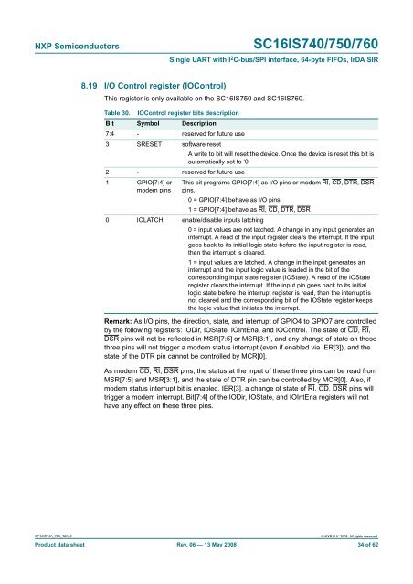
8.19 I/O Control register (IOControl)<br />
This register is only available on the SC16IS<strong>750</strong> and SC16IS<strong>760</strong>.<br />
Table 30. IOControl register bits description<br />
Bit Symbol Description<br />
7:4 - reserved for future use<br />
3 SRESET software reset<br />
A write to bit will reset the device. Once the device is reset this bit is<br />
automatically set to ‘0’<br />
2 - reserved for future use<br />
1 GPIO[7:4] or<br />
modem pins<br />
This bit programs GPIO[7:4] as I/O pins or modem RI, CD, DTR, DSR<br />
pins.<br />
0 = GPIO[7:4] behave as I/O pins<br />
1 = GPIO[7:4] behave as RI, CD, DTR, DSR<br />
0 IOLATCH enable/disable inputs latching<br />
0 = input values are not latched. A change in any input generates an<br />
interrupt. A read of the input register clears the interrupt. If the input<br />
goes back to its initial logic state before the input register is read,<br />
then the interrupt is cleared.<br />
1 = input values are latched. A change in the input generates an<br />
interrupt and the input logic value is loaded in the bit of the<br />
corresponding input state register (IOState). A read of the IOState<br />
register clears the interrupt. If the input pin goes back to its initial<br />
logic state before the interrupt register is read, then the interrupt is<br />
not cleared and the corresponding bit of the IOState register keeps<br />
the logic value that initiates the interrupt.<br />
Remark: As I/O pins, the direction, state, and interrupt of GPIO4 to GPIO7 are controlled<br />
by the following registers: IODir, IOState, IOIntEna, and IOControl. The state of CD, RI,<br />
DSR pins will not be reflected in MSR[7:5] or MSR[3:1], and any change of state on these<br />
three pins will not trigger a modem status interrupt (even if enabled via IER[3]), and the<br />
state of the DTR pin cannot be controlled by MCR[0].<br />
As modem CD, RI, DSR pins, the status at the input of these three pins can be read from<br />
MSR[7:5] and MSR[3:1], and the state of DTR pin can be controlled by MCR[0]. Also, if<br />
modem status interrupt bit is enabled, IER[3], a change of state of RI, CD, DSR pins will<br />
trigger a modem interrupt. Bit[7:4] of the IODir, IOState, and IOIntEna registers will not<br />
have any effect on these three pins.<br />
<strong>SC16IS740</strong>_<strong>750</strong>_<strong>760</strong>_6<br />
© NXP B.V. 2008. All rights reserved.<br />
Product data sheet Rev. 06 — 13 May 2008 34 of 62