Program and Abstract Book - SRON
Program and Abstract Book - SRON
Program and Abstract Book - SRON

You also want an ePaper? Increase the reach of your titles
YUMPU automatically turns print PDFs into web optimized ePapers that Google loves.
19 th International Symposium on Space Terahertz Technology<br />
P5-6<br />
A Novel Thermal Detector for Far-Infrared <strong>and</strong> THZ imaging Arrays<br />
Pekka Rantakari <strong>and</strong> Arttu Luukanen<br />
Millimetre Wave Laboratory of Finl<strong>and</strong> – MilliLab, Espoo, Finl<strong>and</strong><br />
Steven Deiker, Lockheed Martin Solar <strong>and</strong> Astrophysics Laboratory, Palo Alto,<br />
U.S.A.<br />
This paper reports on novel MEMS based thermal detector architecture, which could allow the construction of very<br />
large focal plane arrays of bolometers for far-infrared <strong>and</strong> THz imaging. The principal challenge in developing large<br />
format cryogenic bolometer arrays is related to the multiplexing <strong>and</strong> readout of cryogenic detectors. The readout<br />
architectures that are being developed <strong>and</strong> deployed are mostly based on Superconducting Quantum Interference<br />
Devices (SQUIDs), which are highly sensitive but also relatively complex devices <strong>and</strong> have shortcomings with respect<br />
to the robustness of SQUIDs for operation in nonideal condition.<br />
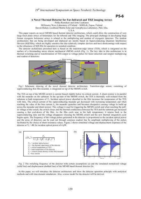
The detector architecture presented here is based on the transition-edge sensor (TES), which is integrated on the<br />
surface of a freest<strong>and</strong>ing micro electro mechanical (MEM) switch (Fig. 1). The key idea in this architecture is in<br />
thermal switching <strong>and</strong> in transformation of TES output to voltage pulses for faster detection <strong>and</strong> simpler multiplexing<br />
<strong>and</strong> readout of detectors.<br />
Shunt resistor<br />
Superconducting me<strong>and</strong>er<br />
I b<br />
I b<br />
MEMS switch<br />
Substrate (T=T b)<br />
Fig.1 Schematic drawing of the novel thermal detector architecture. Transition-edge sensor, consisting of<br />
superconducting thin film me<strong>and</strong>er, is integrated on top of the MEMS switch.<br />
The TES on top of the MEMS switch is current biased slightly below its critical current. A shunt resistor is in parallel<br />
with the me<strong>and</strong>er on the substrate. In the up-state of the MEMS switch, the TES is thermally well-isolated from the<br />
substrate at bath temperature of T b . Incident optical power absorbed to the film increases the temperature of the TES<br />
with time. The critical current of the superconducting me<strong>and</strong>er get decreased with increasing temperature <strong>and</strong> when<br />
reaching the value of the bias current I b , the me<strong>and</strong>er quenches <strong>and</strong> becomes dissipative causing voltage to build up<br />
across the me<strong>and</strong>er <strong>and</strong> shunt resistor. This voltage is used for triggering the MEMS switch <strong>and</strong> when reaching the pullin<br />
voltage of the switch, the switch closes <strong>and</strong> the thermal conductance between the TES <strong>and</strong> the substrate get increased<br />
causing a fast cool-down of the film. As the film cools near to the bath temperature, it returns back to the<br />
superconducting state <strong>and</strong> the voltage disappears releasing the MEMS switch <strong>and</strong> the new thermal integration cycle<br />
begins again. The frequency of the voltage pulses generated in the detector is proportional to the incident optical power<br />
<strong>and</strong> the array of detectors can be read out through common readout line by amplitude multiplexing of the pulses<br />
facilitated by the choice of shunt resistance values. Figure 2 shows simulated voltage <strong>and</strong> displacement responses of the<br />
detector at T b = 4K for incident optical power of 4 pW.<br />
(a)<br />
f<br />
0<br />
( P )<br />
opt<br />
=<br />
T C<br />
P<br />
opt<br />
( −T<br />
T − ( I I ) )<br />
2/3<br />
c th<br />
1<br />
b c b c0<br />
P opt = incident optical power<br />
C th = the thermal capacitance of the detector<br />
T c = critical temperature of TES<br />
T b = bath temperature of the detector<br />
I c0 = critical current density of thin film me<strong>and</strong>er<br />
I b = bias current<br />
(b)<br />
Normalized amplitude<br />
1<br />
0.8<br />
0.6<br />
0.4<br />
0.2<br />
0<br />
-0.2<br />
-0.4<br />
-0.6<br />
-0.8<br />
-1<br />
1 1.5 2 2.5 3 3.5 4 4.5<br />
Time (s)<br />
x 10 -3<br />
Fig. 2 The switching frequency of the detector with certain assumptions (a) <strong>and</strong> the simulated normalized voltage<br />
(solid line) <strong>and</strong> displacement (dodded line) of the MEMS based thermal detector (b).<br />
In this paper, we will introduce the detector architecture <strong>and</strong> show the detector operation principle with analytical<br />
methods <strong>and</strong> with time domain simulations. Also, a noise model for the detector will be derived.<br />
129