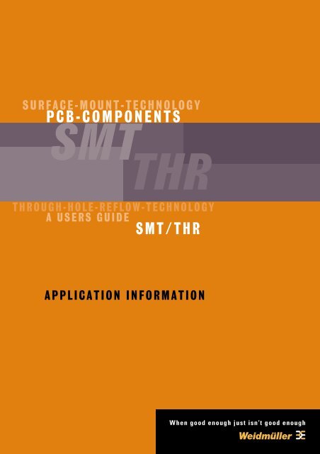
SMT/THR PCB-COMPONENTS
SMT/THR PCB-COMPONENTS
SMT/THR PCB-COMPONENTS

Create successful ePaper yourself
Turn your PDF publications into a flip-book with our unique Google optimized e-Paper software.
SURFACE-MOUNT-TECHNOLOGY<br />
<strong>PCB</strong>-<strong>COMPONENTS</strong><br />
<strong>SMT</strong><br />
<strong>THR</strong><br />
<strong>THR</strong>OUGH-HOLE-REFLOW-TECHNOLOGY<br />
A USERS GUIDE<br />
<strong>SMT</strong>/<strong>THR</strong><br />
APPLICATION INFORMATION
EDITORIAL<br />
EDITORIAL<br />
In the past years, the process of printed circuit board assembly has undergone a<br />
fundamental transformation. Conventional Through-Hole-Technology (THT) has been<br />
increasingly replaced by Surface-Mount-Technology (<strong>SMT</strong>). The reasons for this<br />
were both constantly changing requirements such as miniaturisation of components,<br />
increased density of functions and lower production costs as well as the great<br />
advances achieved in the development of Surface-Mount-Devices (SMD), which only<br />
made use of the <strong>SMT</strong> production process possible at all. Today, <strong>SMT</strong> has established<br />
itself as the standard in printed circuit board (<strong>PCB</strong>) assembly.<br />
But there are still a few components (mainly electromechanical components such as<br />
connectors or relays) which are not available as SMD versions and which, up to now,<br />
still had to be placed on the <strong>PCB</strong> after the actual <strong>SMT</strong> process and in accordance with<br />
the classical THT production method. This is why Weidmüller has developed a product<br />
range for the so-called Through-Hole-Reflow (<strong>THR</strong>) process which makes it possible to<br />
use leaded components in the <strong>SMT</strong> process as well, thus ensuring one hundred percent<br />
consistency in <strong>SMT</strong> production.<br />
With this brochure, we would like to provide you with a practical guide on the basis<br />
of which you can choose the notes on pcb assembly that conform best to your<br />
requirements. The brochure's design does justice to this. If you wish to find out briefly<br />
and concisely what solution or product Weidmüller recommends within the scope of the<br />
technology, then simply read the text in the separate boxes.<br />
2 APPLICATION INFORMATION
TABLE OF CONTENTS<br />
TABLE OF CONTENTS<br />
1 From THT to <strong>SMT</strong> – the evolution of <strong>PCB</strong> assembly 4<br />
2 <strong>THR</strong> – the revolution in <strong>PCB</strong> assembly 5<br />
3 The <strong>SMT</strong> process for modules with <strong>THR</strong> components 6<br />
3.1 The process steps at a glance 6<br />
3.2 Design of the <strong>PCB</strong> and stencil 6<br />
3.3 Paste printing 10<br />
3.4 Placement 12<br />
3.5 Reflow soldering 14<br />
3.6 Quality control 16<br />
4 SL-<strong>SMT</strong> – Weidmüller’s innovative <strong>THR</strong> components 18<br />
for the <strong>SMT</strong> process<br />
APPLICATION INFORMATION 3
1 FROM THT TO <strong>SMT</strong><br />
THE EVOLUTION OF <strong>PCB</strong> ASSEMBLY<br />
THT – assembly with leaded<br />
components<br />
When use is made of Through-Hole-<br />
Technology (THT), which was the<br />
standard process in module production<br />
up to a few years ago, the wire terminals<br />
of the components are inserted into<br />
the holes on the printed circuit board.<br />
Boards are assembled manually or<br />
with special placement machines. The<br />
so-called manual or wave soldering<br />
process is used.<br />
Drawbacks of THT:<br />
• production is time-consuming and<br />
costly<br />
• low function density<br />
• increased susceptibility to faults<br />
due to a lack of manual precision<br />
Single-side <strong>PCB</strong> assembly with<br />
THT components<br />
<strong>SMT</strong> – assembly with<br />
SMD components<br />
With the advent of Surface-Mount-<br />
Devices (SMD), Surface-Mount-<br />
Technology has increasingly taken the<br />
place of THT. And the trend towards<br />
producing electronic modules by surface<br />
mounting is continuing.<br />
As the current standard process in<br />
electronic module production, <strong>SMT</strong> is<br />
defined by the method of processing<br />
components and the soldering process<br />
employed. Thus, when the <strong>SMT</strong> process<br />
is used, <strong>PCB</strong>s can be equipped with SMD<br />
components both on one side and on<br />
both sides. They are assembled with<br />
machines, for example "Pick & Place" or<br />
"Collect & Place" systems, which<br />
process all components in the state in<br />
which they were delivered, dispensing<br />
with special preparation of components.<br />
In the <strong>SMT</strong> process, use is made of<br />
reflow soldering, for example infrared,<br />
convection and vapour phase soldering.<br />
Contrary to the wave soldering process,<br />
only a solder paste deposit applied to the<br />
<strong>PCB</strong> is melted on.<br />
<strong>PCB</strong> double-sided assembly with<br />
SMD components<br />
Advantages of <strong>SMT</strong>:<br />
• high quality<br />
• lower processing cost<br />
• smaller components<br />
• high packing and integration density<br />
• optionally single-sided or doublesided<br />
assembly<br />
<strong>SMT</strong> compatibility in the case of<br />
modules with component mixes<br />
There are still applications in which<br />
SMDs and leaded components have<br />
to be placed on the <strong>PCB</strong>. Up to now,<br />
in the case of modules with such<br />
component mixes use has been made of<br />
two different soldering processes: firstly<br />
reflow soldering for the SMDs followed<br />
by (mostly manual) placement of the<br />
leaded components with subsequent<br />
manual or wave soldering.<br />
<strong>PCB</strong> double-sided mixed assembly with<br />
THT and SMD components<br />
Manual placement and the use of<br />
manual/wave soldering for <strong>SMT</strong><br />
manufactured <strong>PCB</strong>s is a costly and<br />
critical process,<br />
which can lead to<br />
quality defects. There is a need for<br />
achieving consistent <strong>SMT</strong> compatibility,<br />
i.e. making leaded components suitable<br />
for the <strong>SMT</strong> reflow soldering process in<br />
order to reduce manufacturing costs and<br />
to eliminate the wave soldering process,<br />
which is susceptible to faults.<br />
The special process developed for this<br />
purpose is known by various names on<br />
the market, namely Through-Hole-Reflow<br />
(<strong>THR</strong>), Pin-in-Paste (PIP) or Pin-In-Hole-<br />
Intrusive-Reflow (PIHIR).<br />
4 APPLICATION INFORMATION
2 <strong>THR</strong><br />
THE REVOLUTION IN <strong>PCB</strong> ASSEMBLY<br />
Through-Hole-Reflow is a process for<br />
joining THT components using the <strong>SMT</strong><br />
reflow soldering process. In addition to<br />
conventional SMD placement, when <strong>THR</strong><br />
is employed the SMD components are<br />
placed onto the <strong>SMT</strong> board together with<br />
leaded components and are soldered in<br />
the reflow process.<br />
Mechanically not stressable connection: e.g."Gull Wing" type<br />
The <strong>THR</strong> process was the result of the<br />
awareness that stable soldered joints are<br />
still needed for heavy components such<br />
as coils or transformers and wherever<br />
mechanical forces act on the <strong>PCB</strong><br />
(e.g. in the case of connection terminals,<br />
connectors, relay sockets, etc.).<br />
Considering mechanical criteria, SMD<br />
soldered joints are not suitable for heavy<br />
components.<br />
A <strong>SMT</strong> compatible product is always<br />
a compromise between optimum <strong>SMT</strong><br />
capability and maximum stability of the<br />
soldered joint. With push-through pins,<br />
<strong>THR</strong> ensures a stable joint between the<br />
THT components and the <strong>PCB</strong>.<br />
100% <strong>SMT</strong> process compatibility is<br />
achieved at the same time.<br />
Advantages of <strong>THR</strong>:<br />
• stable connection to the <strong>PCB</strong><br />
• only one soldering process<br />
• manual/wave soldering is eliminated<br />
• automatic component placement<br />
• lower production cost<br />
For <strong>THR</strong> components to be processed in<br />
the <strong>SMT</strong> process, certain demands have<br />
to be met. These are described in greater<br />
detail in Chapter 3.<br />
Mechanically stressable connection: THT<br />
APPLICATION INFORMATION 5
3 THE <strong>SMT</strong> PROCESS<br />
FOR MODULES WITH <strong>THR</strong> <strong>COMPONENTS</strong><br />
3.1 The process steps at a glance<br />
1Design-In: design of the <strong>PCB</strong> and<br />
stencil layout for <strong>THR</strong> components<br />
3.2 Design-in<br />
The <strong>SMT</strong> production process begins with<br />
design of the <strong>PCB</strong>. It is as early as in<br />
this first step that the later smooth<br />
sequence of the production process and<br />
thus the quality of the <strong>PCB</strong> assembly<br />
process are defined. In comparison<br />
with the classical SMD or Through-Hole-<br />
Technology, a few special features have<br />
to be observed in the design of <strong>PCB</strong>s<br />
for <strong>THR</strong> components. Special design<br />
recommendations contribute towards<br />
ensuring an optimum production<br />
process.<br />
The design of a printed circuit board<br />
for SMD components is generally very<br />
easy to produce. Once the design of the<br />
soldered joints has been defined, to<br />
avoid process errors the hole layout of<br />
the stencils for paste printing is often<br />
defined about 10% smaller.<br />
By contrast, in the case of <strong>THR</strong><br />
components a drill hole must be filled<br />
with solder paste. In this case, the<br />
quality of the soldering process depends<br />
on what degree of filling of the holes<br />
with solder paste can be achieved in the<br />
printing process.<br />
2Paste printing: solder paste applied<br />
into <strong>THR</strong> placement holes<br />
To optimise the degree of filling,<br />
Weidmüller recommends the following<br />
steps:<br />
3.2.1 define the diameters of placement<br />
holes and soldering eyelets<br />
3Placement: inserting the <strong>THR</strong><br />
component pins in the solder paste<br />
4Reflow soldering: melting on the<br />
solder paste<br />
3.2.2 calculate the solder volume or<br />
the necessary paste volume<br />
3.2.3 determine the degree of solder<br />
paste filling<br />
3.2.4 design the stencil layout<br />
5Quality control: assessment of the<br />
finished <strong>THR</strong> soldered joint<br />
6 APPLICATION INFORMATION
3.2.1 Defining the diameters of<br />
placement holes and soldering<br />
eyelets<br />
To calculate the necessary paste volume,<br />
first define the volume of the soldered<br />
joint in accordance with the required<br />
quality. For an adequate soldered joint,<br />
the internationally recognised quality<br />
standard IPC A610B calls for a 75%<br />
filling height in the <strong>PCB</strong> (see also<br />
Section 3.5 "Quality control").<br />
The designer first defines the relevant<br />
diameter of the placement hole and of<br />
the soldering eyelet. Both parameters<br />
determine the necessary soldering<br />
volume for a given <strong>THR</strong> component.<br />
Placement hole diameter:<br />
For <strong>THR</strong> soldered joints (contrary to<br />
wave soldering), a slightly larger<br />
placement hole diameter is advisable<br />
because melting-on of the paste in the<br />
hole needs sufficient space.<br />
Solder<br />
pastes also consists of a mixture of<br />
soldering globules and admixtures (flux),<br />
and are categorised according to grain<br />
sizes. To avoid jamming or friction of<br />
the pin in the hole with these soldering<br />
globules during the placement process,<br />
the chosen grain size should be as small<br />
as possible.<br />
The tolerances of the <strong>PCB</strong>s, the<br />
placement machine and the component<br />
must be taken into account as further<br />
factors in determining the placement<br />
hole diameter for the automatic<br />
placement process. For example, in<br />
the case of connectors the position of<br />
the pin end in the pitch is subject to<br />
special tolerances, with the result that<br />
it is the respective manufacturer's task<br />
to optimise the pin end position's circle<br />
of throwout.<br />
Weidmüller recommends the following<br />
as suitable placement hole diameters<br />
for <strong>THR</strong> soldering processes:<br />
For round pins:<br />
pin diameter + at least 0.3 mm<br />
For rectangular pins:<br />
pin diameter + at least 0.25 mm<br />
Soldering eyelet diameter:<br />
Soldering eyelet diameter<br />
The volume of the soldering meniscuses<br />
should also be optimised so as to<br />
minimise the solder volume. This is<br />
achieved by minimising the soldering<br />
eyelet diameter in comparison with<br />
diameters as are usual in classical<br />
Through-Hole-Technology.<br />
Recommended soldering eyelet diameter<br />
for through-hole soldered joints:<br />
placement hole diameter<br />
+<br />
2 x residual ring width<br />
=<br />
soldering eyelet diameter<br />
The residual ring width usually amounts<br />
to 0.3 mm. For <strong>THR</strong> components such<br />
as connectors a slight increase in the<br />
residual ring width to about 0.4 mm is<br />
advisable for reasons of higher soldered<br />
joint stability and reparability.<br />
Residual ring<br />
width<br />
Placement hole diameter<br />
Placement hole layout for <strong>THR</strong> pins<br />
APPLICATION INFORMATION 7
3 THE <strong>SMT</strong> PROCESS<br />
FOR MODULES WITH <strong>THR</strong> <strong>COMPONENTS</strong><br />
3.2.2 Calculating the solder volume<br />
or the necessary paste volume<br />
3.2.3 Determining the degree of<br />
solder paste filling<br />
The solder volume that is necessary for<br />
an optimum soldered joint is calculated<br />
as follows:<br />
placement hole volume<br />
+<br />
meniscus volume<br />
–<br />
terminal pin volume<br />
=<br />
solder volume<br />
Solder meniscus<br />
Necessary solder volume for <strong>THR</strong> soldered joint<br />
For an optimum layout of the <strong>PCB</strong>, it<br />
makes sense to check whether the<br />
previously calculated necessary paste<br />
volume can be achieved at all. Therefore,<br />
in a test the degree of solder paste filling<br />
should be determined in a <strong>PCB</strong> hole.<br />
According to the test setting, a test <strong>PCB</strong><br />
with the defined hole diameters, for<br />
example is entered in the paste printing<br />
process. The filling height of the holes in<br />
the <strong>PCB</strong> can then be checked visually.<br />
Pin<br />
Placement hole<br />
Degree of filling approx. 120 %<br />
Determining the degree of filling<br />
3.2.4 Design of the stencil layout<br />
If the optimal degree of solder paste<br />
filling was achieved, the standard design<br />
rule can be used for the stencil hole<br />
design: stencil hole diameter about 10%<br />
smaller then soldering eyelet. Diverse<br />
process parameters contribute towards<br />
a situation in which the degree of hole<br />
filling is not achieved. In this case,<br />
several possibilities of optimising the<br />
degree of filling are at the printed<br />
circuit board designer's disposal:<br />
Once the solder volume has been<br />
determined, the necessary paste volume<br />
can also be calculated. Due to the high<br />
evaporation factor of the solder paste in<br />
the soldering process (generally about<br />
50%), it amounts to approximately twice<br />
the volume:<br />
paste volume<br />
=<br />
solder volume x 2<br />
The following applies:<br />
100% filling of the <strong>PCB</strong>s thickness<br />
=<br />
100% degree of filling<br />
• optimising the printing parameters<br />
(see Section 3.3 "Paste printing")<br />
• optimising the stencil layout: If there<br />
is not enough paste, printing over the<br />
soldering eyelet is advisable. Various<br />
forms of asymmetrical printing can<br />
also be applied. As an alternative,<br />
stepped and additive stencils or<br />
double printing by means of<br />
extremely thick stencils can also<br />
be applied. If there is too much paste,<br />
webs over the breakouts of the stencil<br />
may function as a paste brake.<br />
8 APPLICATION INFORMATION
Additional design factors :<br />
Stencil hole diameter<br />
For a smooth <strong>SMT</strong> production process,<br />
the following factors should also be<br />
observed when designing a module:<br />
• shadow formation in the reflow<br />
oven, caused by high housings of<br />
the <strong>THR</strong> components, can be avoided<br />
by an adequate distance between the<br />
components<br />
• the components' contact faces must<br />
be taken into account to ensure that<br />
the insulator does not come into<br />
contact with the paste<br />
• fixing by glueing may be necessary<br />
if, in the case of double-sided<br />
modules, a <strong>THR</strong> component is placed<br />
on the first placement side<br />
Stencil hole layout assuming adequate degree of paste filling<br />
Stencil hole diameter about<br />
10% smaller than soldering<br />
eyelet diameter<br />
Solutions and recommendations from Weidmüller<br />
In a first draft of the printed circuit board and stencil layout, you can safely work<br />
with the known standard process parameters.<br />
For their SL-<strong>SMT</strong> pin headers with short pins (1.5 mm), Weidmüller suggests the<br />
following <strong>PCB</strong> design:<br />
Placement hole diameter: 1.5 mm<br />
Soldering eyelet diameter: 2.3 mm<br />
Stencil hole diameter: 2.1 mm (assuming adequate degree of paste filling)<br />
Stencil hole diameter: 2.8 mm (if the degree of paste filling is not enough)<br />
Valid for:<br />
<strong>PCB</strong> thickness: 1.5 - 1.6 mm<br />
Stencil thickness: 0.12 - 0.18 mm<br />
APPLICATION INFORMATION 9
3 THE <strong>SMT</strong> PROCESS<br />
FOR MODULES WITH <strong>THR</strong> <strong>COMPONENTS</strong><br />
3.3 Paste printings<br />
Preparation of the <strong>PCB</strong>, i.e. applying<br />
solder paste on the soldering pads, is<br />
one of the most important steps in the<br />
<strong>SMT</strong> production process. The quality<br />
achieved here has a crucial influence<br />
on the quality of all further process<br />
steps. The soldering result in the<br />
subsequent placement and reflow<br />
process is determined by the necessary<br />
paste volume and thus the degree<br />
of solder paste filling during paste<br />
application. For optimum filling of the<br />
<strong>THR</strong> holes within the usual process<br />
tolerances, printing of the solder paste in<br />
two different stencil printing processes<br />
has asserted itself, namely the open and<br />
closed stencil printing processes.<br />
In the open stencil printing process,<br />
a metal or plastic squeegee pushes the<br />
roll of solder paste over the stencil.<br />
The drawback of this process is that both<br />
the pressure and the printing speed<br />
can only be varied within a very limited<br />
range.<br />
Open stencil printing process<br />
In closed printing systems such as<br />
"ProFlow", however, a paste deposit with<br />
a variably adjustable pressure travels<br />
over the stencil. The advantage: better<br />
monitoring of the pressure and printing<br />
speed permits paste printing by High-<br />
Speed Fine-Pitch Technology as well as<br />
controlled filling of the <strong>THR</strong> hole. Various<br />
stencil variants can be used depending<br />
on the chosen technology, namely the<br />
low-cost standard metal stencils or even<br />
expensive "exotic" variants such as<br />
stepped or double printing stencils.<br />
For an optimum degree of solder paste<br />
filling, the following process parameters<br />
must be taken into account in the paste<br />
printing process:<br />
• stencil thickness:<br />
generally 120 to 200 µm<br />
• optimum coordination of the solder<br />
paste grain size (20-40 µm) and<br />
volume percentage of the flux<br />
(mostly 50%)<br />
• coordination of squeegee speed and<br />
pressure: a higher degree of filling<br />
with open paste systems is achieved<br />
by a lower speed or a flatter angle<br />
(e.g. 45° instead of 60°)<br />
Pin header (open and closed ended): 2 to 8 poles 9 to 24 poles<br />
Pin header (flanged LF):<br />
2 to 24 poles<br />
recommended inside diameter d I = 1.4 +0.1 mm d I = 1.5 +0.1 mm<br />
finished hole *1):<br />
paste volume VP [mm 3 ] /<br />
filling level fp [%] after print<br />
minimum solder joint shape 2.4 mm 3 / 70 % 3.1 mm 3 / 85 %<br />
optimum solder joint shape 2.9 mm 3 / 90 % 3.5 mm 3 / 100 %<br />
Example of a recommended paste volume or degree of filling for SL-<strong>SMT</strong> pin headers accord. to data sheet<br />
10 APPLICATION INFORMATION
Various requirements for the leaded<br />
components can now be derived from<br />
these parameters:<br />
• as the housing of the leaded<br />
component must not touch the solder<br />
paste, its stand-off height should be<br />
at least 0.3 mm<br />
• the pin cross-section geometry, the<br />
pin tip and its length must be<br />
optimised to minimise the paste<br />
volume needed<br />
If the degree of solder paste filling is too<br />
low, then it is advisable to overprint to<br />
achieve the necessary paste volume.<br />
Overprinting means that the stencil hole<br />
diameter is designed to be larger than<br />
the soldering eyelet diameter and the<br />
paste is printed over an area larger than<br />
the soldering eyelet, and out onto the<br />
<strong>PCB</strong>. This can, of course, cause soiling<br />
of the underside of the stencil, which<br />
can be removed by a shorter cleaning<br />
cycle of the stencil.<br />
Overprinting can lead to soiling of the underside of the stencil<br />
Solutions and recommendations from Weidmüller<br />
To realise the lowest possible paste volume in stencil printing, the SL-<strong>SMT</strong> pin<br />
headers from Weidmüller feature short octagonal pins with chamfered pin ends.<br />
Above all thanks to the pin length of only 1.5 mm for standard pc boards with a<br />
thickness of 1.6 mm, a filling degree of 90 % only is adequate for an optimal solder<br />
joint shape. Therefore in most cases normal single-layer stencils for fine-pitch<br />
technology and the standard process parameters for the squeegee speed and<br />
pressure can be used during paste printing.<br />
Further advantage: in the placement process, the paste is forced out of the<br />
placement hole to a lesser extent.<br />
APPLICATION INFORMATION 11
3 THE <strong>SMT</strong> PROCESS<br />
FOR MODULES WITH <strong>THR</strong> <strong>COMPONENTS</strong><br />
3.4 The placement process<br />
Automatic sequential placement is one of<br />
the placement processes that is used<br />
most frequently in the <strong>SMT</strong> process. Use<br />
is made of both pick & place systems<br />
and of collect & place systems (chip<br />
shooter). In the pick & place station, only<br />
one components is taken from the<br />
component feeder by means of a vacuum<br />
pipette, and is placed on the pcb.<br />
Pick & Place head transports SL-<strong>SMT</strong> 3.5<br />
By contrast, a chip shooter transports<br />
several components to the corresponding<br />
placement position and deposits them<br />
there.<br />
Packaging of the components is the<br />
basis for the use of both processes.<br />
A distinction is made between tape-onreel,<br />
tray, tube and bulk. The pick & place<br />
process with tape-on-reel or tray has<br />
established itself for leaded terminal<br />
elements.<br />
The following parameters must be<br />
observed with regard to the optimum<br />
placement suitability of leaded terminal<br />
elements and thus easy integration<br />
into the placement process with usual<br />
standard placement systems:<br />
Tray packaging accord. to IEC 286-5<br />
• packaging in line with standards:<br />
fully automatic feeding of the<br />
terminal elements with tape-on-reel<br />
or tray is possible<br />
• dimensional stability of the<br />
component: lowest possible water<br />
absorption during storage under<br />
normal climatic conditions ensuring<br />
pitch fidelity of the component<br />
• suction surface of the component:<br />
determined in relation to the weight<br />
or size for the use of standardised<br />
vacuum nozzles<br />
• precision of the pin end position:<br />
smallest possible tolerances<br />
(in addition to hole position and<br />
machine placement tolerance)<br />
prevent problems caused by collision<br />
of the component with the <strong>PCB</strong><br />
This results in the following<br />
requirements for leaded terminal<br />
elements:<br />
• minimised weight for an placement<br />
speed that is as high as possible<br />
• minimised component length for a<br />
high rotation and transport speed<br />
and thus maximum placement<br />
performance<br />
• minimised height to avoid a<br />
restriction of the travel height<br />
over the <strong>PCB</strong> and thus to prevent<br />
collisions<br />
Tape-on-reel packaging accord. to IEC 286-3<br />
• minimised tooling effort by using<br />
components in high packed numbers<br />
to achieve lower product and tooling<br />
costs<br />
12 APPLICATION INFORMATION
%<br />
Changes in length because<br />
of water absorption<br />
1.0<br />
0.03<br />
PA 4.6: 1 % => 0.5 mm / 50 mm =><br />
„50.5“ mm (total length for a 10 pole pin header)<br />
50.5<br />
LCP: 0.03 % => 0.015 mm / 50 mm =><br />
„50.015“ mm (total length for a 10 pole pin header)<br />
50.015<br />
mm<br />
Total length for a 10 pole pin header with pitch 5.00 mm<br />
Pin header SL-<strong>SMT</strong> with<br />
pick & place pad<br />
Dimension changes because of water absorption for different materials.<br />
Solutions and recommendations from Weidmüller<br />
To avoid quality-reducing dimensional changes, the SL-<strong>SMT</strong> pin headers from<br />
Weidmüller are made of LCP (Liquid Crystal Polymer). LCP is particularly<br />
distinguished by very low water absorption.<br />
The SL-<strong>SMT</strong> pin headers have a low height thanks to the use of short pins (1.5 mm).<br />
This is why the height of the tape-on-reel or tray packaging can also be very low.<br />
The result: a large number of packaged units in each reel. The antistatic packaging<br />
in line with standards also permits fully automatic placement using commercially<br />
available pick & place systems.<br />
Further advantages of the short pins of the SL-<strong>SMT</strong> are optimised travel height<br />
and the precision of the pin end position, thus avoiding collisions between the<br />
components and the <strong>PCB</strong>. And, as the <strong>SMT</strong>-optimised pin headers from Weidmüller<br />
are very light, they also maximise placement performance.<br />
APPLICATION INFORMATION 13
3 THE <strong>SMT</strong> PROCESS<br />
FOR MODULES WITH <strong>THR</strong> <strong>COMPONENTS</strong><br />
3.5 Reflow soldering<br />
The most important step in the <strong>SMT</strong><br />
production process besides paste<br />
printing is the reflow soldering process.<br />
This process is characterised by melting<br />
of an existing solder deposit. During the<br />
process about 50% of the paste volume<br />
evaporates. The aim of reflow soldering<br />
is to enable soldering of all <strong>THR</strong> joints in<br />
all soldering processes.<br />
Currently three different reflow soldering<br />
processes are needed in industrial<br />
applications:<br />
• Infrared soldering:<br />
exploits heat radiation with natural<br />
convection, as generated by quartz<br />
or area radiators, for example, to heat<br />
the module.<br />
• Convection soldering:<br />
heats up the module by force<br />
convection by means of the<br />
circulation of large volumes of a<br />
Each of the three processes calls for a<br />
special process temperature curve,<br />
which also applies to <strong>THR</strong> components.<br />
As increased use will be made of<br />
unleaded soldering processes with<br />
increased temperatures in the future,<br />
the demands on the temperature load<br />
carrying capacity of components will<br />
continue to rise.<br />
For use in the reflow soldering process,<br />
the following factors or requirements are<br />
crucial in regards to <strong>THR</strong> components:<br />
• Soldering heat resistance:<br />
the shape and the functionality of the<br />
component must not be damaged by<br />
the soldering process. In this respect,<br />
all components can be checked with<br />
a test method that is described in<br />
EN 61760-1. This process permits the<br />
measurement of <strong>THR</strong> component’s<br />
thermal resistance by means of a<br />
simulation.<br />
Soldering heat resistance is tested for<br />
the highest category A, by dipping the<br />
component in a soldering bath:<br />
The insulator floats on the surface of<br />
the solder and all soldering contacts<br />
are immersed. The minimum<br />
requirement is 260 °C/10 sec.<br />
Melted isolation body due to inadequat thermal<br />
resistance of the plastic<br />
Moreover, the component's suitability<br />
for passing through the soldering<br />
process twice (double-sided<br />
assembly) must be guaranteed.<br />
process gas such as air or nitrogen.<br />
• Vapour phase soldering:<br />
uses a condensating saturated<br />
Temperature (°C)<br />
240° C<br />
230° C<br />
215° C<br />
Melting<br />
vapour phase as the transmission<br />
medium which dissipates its<br />
condensation heat directly to the<br />
surface of the medium.<br />
180° C<br />
Pre-heating<br />
160° C<br />
150° C<br />
130° C<br />
Approx. 60sec<br />
> 180° C<br />
Usual<br />
Time (sec)<br />
Infrared soldering, convection soldering – temperature/time diagram (temperature on connection)<br />
14 APPLICATION INFORMATION
• Thermal coefficient of expansion:<br />
very long components such as<br />
multiple-pin connectors, which<br />
exhibit a significantly different<br />
thermal response to that of the <strong>PCB</strong><br />
material may lead to sagging of the<br />
module after soldering or in the<br />
cooling phase. To avoid this problem,<br />
the temperature response of the<br />
components and <strong>PCB</strong> materials<br />
should be as similar as possible.<br />
Usual materials such as PBT or<br />
PA 6.6, which are used in connectors<br />
designed for wave soldering<br />
processes are therefore not suitable<br />
for reflow processes.<br />
• Solution:<br />
make components out of highly<br />
temperature-resistant plastics with<br />
low water absorption.<br />
Even if apparently all factors and<br />
requirements for the components<br />
participating in the reflow soldering<br />
process have been met, though, in some<br />
cases the desired production quality<br />
cannot be achieved.<br />
The most frequent sources of faults are:<br />
• Errors in component design:<br />
accessibility of the soldered joints for<br />
the thermal transmission medium<br />
(e.g. air) is restricted by neighbouring<br />
components. This can, however, be<br />
defined in advance by means of an<br />
appropriate component design.<br />
• Errors in <strong>PCB</strong> design:<br />
copper terminal faces that are too<br />
large lead to heat sinks on the<br />
soldering eyelets.<br />
• Faults of the soldering machine:<br />
the melting temperature that is<br />
necessary for the solder paste at<br />
the soldered joint is not reached<br />
due to inadequate efficiency of the<br />
reflow soldering machine or of the<br />
programmed process profile.<br />
Solutions and recommendations from Weidmüller<br />
Weidmüller manufactures long components such as multiple-pin pin headers out of<br />
fibre-glass reinforced LCP (Liquid Crystal Polymer). This high temperature-resistant,<br />
Melted isolation body due to inadequat thermal<br />
resistance of the plastic<br />
• Water content:<br />
only components made of insulators<br />
with minimum water absorption<br />
prevent bubble formation during the<br />
soldering process and thus<br />
modification of the insulator's<br />
surface.<br />
halogen-free insulator has a melting point of 335 °C and therefore exhibits high<br />
stability of shape and very good soldering heat resistance. Weidmüller surpasses<br />
EN 61760-1 and subjects its terminal elements to 2 x 260 °C/10 sec. for a double<br />
passage through the process. The SL-<strong>SMT</strong> pin headers made of LCP even withstand<br />
2 x 290 °C/30 sec. and are therefore oriented to the future and can also be used in<br />
every lead-free soldering process.<br />
One further advantage of LCP is its extremely low thermal coefficient of expansion.<br />
Measured on the SL-<strong>SMT</strong> pin header from Weidmüller, it amounts to 0.16% at<br />
260 °C = 0.08 mm for a length of 50 mm, for example.<br />
It therefore exhibits a thermal response that is similar to that of common <strong>PCB</strong> base<br />
material, for example FR4, with the result that sagging of a pcb after the soldering<br />
process is avoided in any case.<br />
APPLICATION INFORMATION 15
3 THE <strong>SMT</strong> PROCESS<br />
FOR MODULES WITH <strong>THR</strong> <strong>COMPONENTS</strong><br />
3.6 Quality control<br />
Quality control concludes the <strong>SMT</strong><br />
production process. The aim of this<br />
process step is to enable swift and<br />
simple assessment, by suitable means,<br />
of the quality of the soldered joints of<br />
<strong>THR</strong> components with short or long pins.<br />
The same rules apply to quality control of<br />
the <strong>THR</strong> technology as to reflow or wavesoldered<br />
THT components.<br />
Inspection method:<br />
Quality control in parallel with the<br />
process can be realised by means of<br />
different processes. At the moment,<br />
mostly optical or X-ray inspection is<br />
used. The optical test evaluates the<br />
shape, reflection and colour of soldered<br />
joints.<br />
In the case of X-ray inspection,<br />
so-called radiographic evaluation is<br />
run by means of an automated X-ray<br />
microscope. In addition the inspection<br />
processes during the production process,<br />
an important inspection step consists<br />
of destruction tests. Carried out on<br />
samples, they serve to check measurable<br />
quantities:<br />
Cross-section of the <strong>THR</strong>-solder joint<br />
with short pin<br />
• analysis of the degree of filling by<br />
means of a cross-section through the<br />
soldered joint<br />
• mechanical inspection of the force<br />
needed to pull the pins out of the<br />
through plated holes<br />
a<br />
Standards:<br />
Various standards have come into force<br />
in the past years to enable objective<br />
quality control. Besides other acceptance<br />
test criteria for the production quality<br />
of electronic modules, the assessment<br />
criteria based on the IPC-A-610B have<br />
been acknowledged the world over.<br />
According to IPC-A-610B, the quality<br />
requirements for <strong>THR</strong> soldered joints are<br />
subdivided into three categories.<br />
Generally the requirements of category 3<br />
are decisive for high-power electronics<br />
in industrial applications. The following<br />
values have been defined for the total<br />
number of five assessment criteria:<br />
• circumferential wetting of the<br />
primary side (i.e. the component<br />
side from the component's point of<br />
view), the terminal and the sleeve<br />
must not fall below 270°<br />
• vertical solder filling must be<br />
at least 75%<br />
Optical test of soldered joints below the<br />
housing body.<br />
When done manually, a magnifying<br />
glass or a microscope is used and, in<br />
the automated process, a computercontrolled<br />
camera performs computerassisted<br />
image evaluation.<br />
75 %<br />
Dimensioning the filling height for through-hole soldered joints in accordance with IPC-A-610B<br />
16 APPLICATION INFORMATION
• circumferential wetting of the<br />
secondary side (i.e. underside from<br />
the point of view of the component)<br />
must not fall below 330°<br />
• solder wetting of the original land<br />
face (i.e. residual ring in the case of<br />
<strong>THR</strong> soldered joints) on the primary<br />
side is defined as 0%<br />
• solder wetting of the original land<br />
face on the secondary side must be<br />
at least 75%<br />
With regard to quality control, these<br />
standards result in several requirements<br />
for leaded components. It is necessary<br />
to take into account the fact the two<br />
different designs are normally used for<br />
the <strong>THR</strong> process:<br />
• shorter pins in comparison with the<br />
<strong>PCB</strong>s thickness<br />
• longer pins in comparison with<br />
the <strong>PCB</strong>s thickness (approx.<br />
1.0 – 1.5 mm overhang)<br />
The following requirements apply in the<br />
case of short pins:<br />
• the soldered joints on the primary<br />
side of the <strong>PCB</strong> must be visible<br />
• in the case of components with pins<br />
under the insulator, the height of the<br />
stand-off or the product design must<br />
be adequately dimensioned for visual<br />
inspection<br />
These requirements apply to long pins:<br />
• the soldered joints on the secondary<br />
side must be visible<br />
• by comparison, soldered joints on<br />
the primary side are not necessary<br />
In the case of destructive inspections<br />
in conjunction with <strong>THR</strong> components,<br />
demands are also placed on the <strong>PCB</strong>.<br />
The force needed to pull the pins out of<br />
the soldered joint is checked to ensure<br />
the quality of <strong>PCB</strong> production:<br />
Required pull-out force:<br />
- for short pins: approx. > 150 N<br />
- for long pins with solder meniscus on<br />
the primary and secondary sides:<br />
approx. > 220 N<br />
Solutions and recommendations from Weidmüller<br />
Short pin pulled out with pull-out<br />
force of >150N<br />
Short pins with a solder meniscus only on the primary side attains a comparably<br />
high stability which is otherwise only possible when using the conventional THT.<br />
Hence <strong>THR</strong> components - like Weidmüllers SL-<strong>SMT</strong> - fitted with short <strong>THR</strong> pins have<br />
a considerable advantage over real surface-mount connections.<br />
The special design of the SL-<strong>SMT</strong> pin headers from Weidmüller permits visual<br />
inspection of a <strong>PCB</strong>s primary side, even in the case of variants with an 180°<br />
outgoing direction, thus creating the prerequisite for quality control in parallel<br />
with the process.<br />
However it is important that the control side of the components is not concealed by<br />
other high elements. Weidmüller recommends therefore, during the layout of the<br />
<strong>PCB</strong>, to take into consideration the placement possibilities of the components on the<br />
primary or quality inspection side.<br />
For comparison:<br />
in the case of surface connections with<br />
SMD components, the required pull-out<br />
force amounts only to about 15 – 20 N.<br />
APPLICATION INFORMATION 17
4 SL-<strong>SMT</strong> – WEIDMÜLLER'S INNOVATIVE<br />
<strong>THR</strong> <strong>COMPONENTS</strong> FOR THE <strong>SMT</strong> PROCESS<br />
The new standard in the <strong>SMT</strong> process<br />
of printed circuit board assembly comes<br />
from Weidmüller: the SL-<strong>SMT</strong> pin<br />
headers. Every SL-<strong>SMT</strong> pin header<br />
incorporates Weidmüller's many years<br />
of experience in the <strong>SMT</strong> production<br />
process and the concentrated knowhow<br />
about what demands it places<br />
on <strong>THR</strong> components. This is why<br />
SL-<strong>SMT</strong> pin headers not only fulfill<br />
these requirements, they also offer<br />
you the optimum workflow in automatic<br />
two-sided <strong>PCB</strong> assembly, thus reducing<br />
your production costs by up to 30%.<br />
SL-<strong>SMT</strong> are consistent!<br />
SL-<strong>SMT</strong> are made of high-grade LCP<br />
(Liquid Crystal Polymer).<br />
Your advantages:<br />
• maximum pitch fidelity and<br />
dimensional stability in the<br />
placement process<br />
• thermal response similar to that<br />
of common <strong>PCB</strong> materials<br />
• temperature-resistant for all<br />
common soldering processes<br />
• maximum orientation to the future:<br />
halogen-free and capable of recycling<br />
• maximum design flexibility: available<br />
in versions from 2 to 24 pins<br />
SL-<strong>SMT</strong> are extraordinary!<br />
SL-<strong>SMT</strong> use short pins with a length<br />
of only 1.5 mm.<br />
Your advantages:<br />
• double-sided <strong>SMT</strong> placement with<br />
a <strong>PCB</strong> thickness >= 1.5 mm<br />
• required paste volume minimised<br />
• simplified paste printing process<br />
• no-problem outgassing of the flux<br />
in the soldering process<br />
1.5 mm<br />
2 to 24 poles<br />
• guaranteed assumption of the<br />
necessary temperature in the<br />
soldering process thanks to a<br />
reduced metal mass<br />
• lower component height avoids<br />
collisions in the placement process<br />
• reduced packaging height permits<br />
the use of standard feeders<br />
• optimised quantity in each packaged<br />
reel<br />
18 APPLICATION INFORMATION
SL-<strong>SMT</strong> are innovative!<br />
SL-<strong>SMT</strong> feature an integrated paste<br />
space with stand-off height of at<br />
least 0.3 mm.<br />
0.3 mm<br />
Your advantages:<br />
• very simple stencil design for<br />
standard layout or for printing over<br />
• design-compatible with standard pin<br />
headers because there is no<br />
additional stand-off<br />
• optimised stability in the soldered<br />
joint in comparison with round pins<br />
• minimisation of the placement force<br />
needed, for setting the pins<br />
into the paste by the placement<br />
machines<br />
Optimised pin tip<br />
SL-<strong>SMT</strong> are intelligent!<br />
SL-<strong>SMT</strong> are obtainable in the intelligent<br />
packaging design – suitable for several<br />
pin number variants.<br />
Your advantages:<br />
• only one feeder width is necessary<br />
for several pole numbers<br />
• compatible with all common<br />
pick & place placement systems<br />
• lowest possible packaging heigth<br />
for a higher quantity per reel<br />
• antistatic ESD materials for<br />
problem-free placement<br />
SL-<strong>SMT</strong> are application-optimised!<br />
Pin header with 180° outgoing direction<br />
and open ends: SL-<strong>SMT</strong> 5.08/8/180<br />
SL-<strong>SMT</strong> feature octagonal pins which are<br />
specially designed at the ends.<br />
Your advantages:<br />
• minimisation of the necessary<br />
through hole diameter and thus<br />
of the necessary paste volume<br />
• better recognition in vision<br />
systems thanks to enlarged<br />
reflection faces<br />
Product specific packaging design<br />
APPLICATION INFORMATION 19
Argentina<br />
Australia<br />
Austria<br />
Bahrain<br />
Belarus<br />
Belgium<br />
Brazil<br />
Bulgaria<br />
Canada<br />
Chile<br />
China<br />
Colombia<br />
Costa Rica<br />
Croatia<br />
Czech Republic<br />
Denmark<br />
Egypt<br />
El Salvador<br />
Estonia<br />
Finland<br />
France<br />
Germany<br />
Greece<br />
Guatemala<br />
Honduras<br />
Hong Kong<br />
Hungary<br />
India<br />
Indonesia<br />
Iran<br />
Ireland<br />
Israel<br />
Italy<br />
Japan<br />
Jordan<br />
Kuwait<br />
Lebanon<br />
Luxembourg<br />
Malaysia<br />
Mexico<br />
Morocco<br />
Netherlands<br />
New Zealand<br />
Nicaragua<br />
Norway<br />
Oman<br />
Pakistan<br />
Panama<br />
Peru<br />
Philippines<br />
Poland<br />
Portugal<br />
Qatar<br />
Romania<br />
Russia<br />
Saudi Arabia<br />
Singapore<br />
Slovakia<br />
Slovenia<br />
South Africa<br />
South Korea<br />
Spain<br />
Sweden<br />
Switzerland<br />
Syria<br />
Taiwan<br />
Thailand<br />
Turkey<br />
Ukraine<br />
United Arab Emirates<br />
United Kingdom<br />
USA<br />
Vietnam<br />
Yemen<br />
Yugoslavia<br />
www.weidmueller.com www.weidmueller.com<br />
www.weidmueller.com<br />
Weidmüller is the leading manufacturer<br />
of components for electrical<br />
connection technology.<br />
We develop, produce and sell a wide<br />
spectrum of products from terminal<br />
blocks through connectors to relay<br />
sockets and I/O sockets for every<br />
type of application.<br />
'!0D22EI-c88830<br />
Order number:<br />
5628740000/06/2002/BKD/Bö.