SMT/THR PCB-COMPONENTS
SMT/THR PCB-COMPONENTS
SMT/THR PCB-COMPONENTS

You also want an ePaper? Increase the reach of your titles
YUMPU automatically turns print PDFs into web optimized ePapers that Google loves.
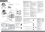
3 THE <strong>SMT</strong> PROCESS<br />
FOR MODULES WITH <strong>THR</strong> <strong>COMPONENTS</strong><br />
3.4 The placement process<br />
Automatic sequential placement is one of<br />
the placement processes that is used<br />
most frequently in the <strong>SMT</strong> process. Use<br />
is made of both pick & place systems<br />
and of collect & place systems (chip<br />
shooter). In the pick & place station, only<br />
one components is taken from the<br />
component feeder by means of a vacuum<br />
pipette, and is placed on the pcb.<br />
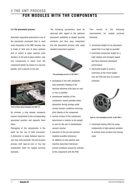
Pick & Place head transports SL-<strong>SMT</strong> 3.5<br />
By contrast, a chip shooter transports<br />
several components to the corresponding<br />
placement position and deposits them<br />
there.<br />
Packaging of the components is the<br />
basis for the use of both processes.<br />
A distinction is made between tape-onreel,<br />
tray, tube and bulk. The pick & place<br />
process with tape-on-reel or tray has<br />
established itself for leaded terminal<br />
elements.<br />
The following parameters must be<br />
observed with regard to the optimum<br />
placement suitability of leaded terminal<br />
elements and thus easy integration<br />
into the placement process with usual<br />
standard placement systems:<br />
Tray packaging accord. to IEC 286-5<br />
• packaging in line with standards:<br />
fully automatic feeding of the<br />
terminal elements with tape-on-reel<br />
or tray is possible<br />
• dimensional stability of the<br />
component: lowest possible water<br />
absorption during storage under<br />
normal climatic conditions ensuring<br />
pitch fidelity of the component<br />
• suction surface of the component:<br />
determined in relation to the weight<br />
or size for the use of standardised<br />
vacuum nozzles<br />
• precision of the pin end position:<br />
smallest possible tolerances<br />
(in addition to hole position and<br />
machine placement tolerance)<br />
prevent problems caused by collision<br />
of the component with the <strong>PCB</strong><br />
This results in the following<br />
requirements for leaded terminal<br />
elements:<br />
• minimised weight for an placement<br />
speed that is as high as possible<br />
• minimised component length for a<br />
high rotation and transport speed<br />
and thus maximum placement<br />
performance<br />
• minimised height to avoid a<br />
restriction of the travel height<br />
over the <strong>PCB</strong> and thus to prevent<br />
collisions<br />
Tape-on-reel packaging accord. to IEC 286-3<br />
• minimised tooling effort by using<br />
components in high packed numbers<br />
to achieve lower product and tooling<br />
costs<br />
12 APPLICATION INFORMATION