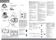
SMT/THR PCB-COMPONENTS
SMT/THR PCB-COMPONENTS
SMT/THR PCB-COMPONENTS

You also want an ePaper? Increase the reach of your titles
YUMPU automatically turns print PDFs into web optimized ePapers that Google loves.
3 THE <strong>SMT</strong> PROCESS<br />
FOR MODULES WITH <strong>THR</strong> <strong>COMPONENTS</strong><br />
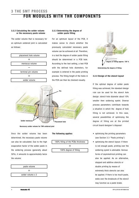
3.2.2 Calculating the solder volume<br />
or the necessary paste volume<br />
3.2.3 Determining the degree of<br />
solder paste filling<br />
The solder volume that is necessary for<br />
an optimum soldered joint is calculated<br />
as follows:<br />
placement hole volume<br />
+<br />
meniscus volume<br />
–<br />
terminal pin volume<br />
=<br />
solder volume<br />
Solder meniscus<br />
Necessary solder volume for <strong>THR</strong> soldered joint<br />
For an optimum layout of the <strong>PCB</strong>, it<br />
makes sense to check whether the<br />
previously calculated necessary paste<br />
volume can be achieved at all. Therefore,<br />
in a test the degree of solder paste filling<br />
should be determined in a <strong>PCB</strong> hole.<br />
According to the test setting, a test <strong>PCB</strong><br />
with the defined hole diameters, for<br />
example is entered in the paste printing<br />
process. The filling height of the holes in<br />
the <strong>PCB</strong> can then be checked visually.<br />
Pin<br />
Placement hole<br />
Degree of filling approx. 120 %<br />
Determining the degree of filling<br />
3.2.4 Design of the stencil layout<br />
If the optimal degree of solder paste<br />
filling was achieved, the standard design<br />
rule can be used for the stencil hole<br />
design: stencil hole diameter about 10%<br />
smaller then soldering eyelet. Diverse<br />
process parameters contribute towards<br />
a situation in which the degree of hole<br />
filling is not achieved. In this case,<br />
several possibilities of optimising the<br />
degree of filling are at the printed<br />
circuit board designer's disposal:<br />
Once the solder volume has been<br />
determined, the necessary paste volume<br />
can also be calculated. Due to the high<br />
evaporation factor of the solder paste in<br />
the soldering process (generally about<br />
50%), it amounts to approximately twice<br />
the volume:<br />
paste volume<br />
=<br />
solder volume x 2<br />
The following applies:<br />
100% filling of the <strong>PCB</strong>s thickness<br />
=<br />
100% degree of filling<br />
• optimising the printing parameters<br />
(see Section 3.3 "Paste printing")<br />
• optimising the stencil layout: If there<br />
is not enough paste, printing over the<br />
soldering eyelet is advisable. Various<br />
forms of asymmetrical printing can<br />
also be applied. As an alternative,<br />
stepped and additive stencils or<br />
double printing by means of<br />
extremely thick stencils can also<br />
be applied. If there is too much paste,<br />
webs over the breakouts of the stencil<br />
may function as a paste brake.<br />
8 APPLICATION INFORMATION