FALCOM JP18 GPS receiver - Hardware manual
FALCOM JP18 GPS receiver - Hardware manual
FALCOM JP18 GPS receiver - Hardware manual

Create successful ePaper yourself
Turn your PDF publications into a flip-book with our unique Google optimized e-Paper software.
<strong>JP18</strong> <strong>FALCOM</strong> <strong>GPS</strong> RECEIVER VERSION 1.0.7<br />
6 HARDWARE INTERFACE AND CONFIGURATION<br />
SIGNALS<br />
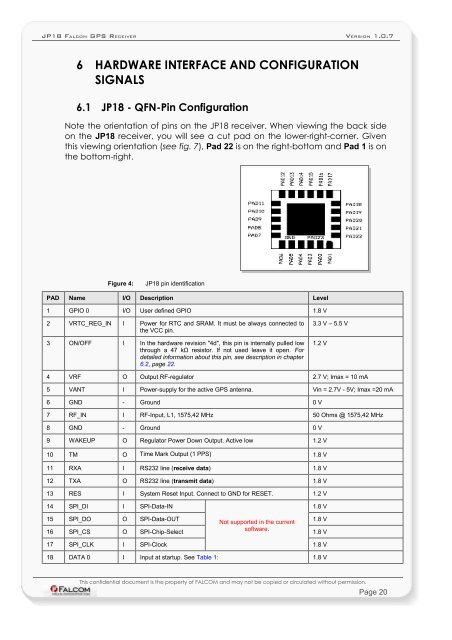
6.1 <strong>JP18</strong> - QFN-Pin Configuration<br />
Note the orientation of pins on the <strong>JP18</strong> <strong>receiver</strong>. When viewing the back side<br />
on the <strong>JP18</strong> <strong>receiver</strong>, you will see a cut pad on the lower-right-corner. Given<br />
this viewing orientation (see fig. 7), Pad 22 is on the right-bottom and Pad 1 is on<br />
the bottom-right.<br />
Figure 4: <strong>JP18</strong> pin identification<br />
PAD Name I/O Description Level<br />
1 GPIO 0 I/O User defined GPIO 1.8 V<br />
2 VRTC_REG_IN I Power for RTC and SRAM. It must be always connected to<br />
the VCC pin.<br />
3 ON/OFF I In the hardware revision "4d", this pin is internally pulled low<br />
through a 47 kΩ resistor. If not used leave it open. For<br />
detailed information about this pin, see description in chapter<br />
6.2, page 22.<br />
3.3 V – 5.5 V<br />
4 VRF O Output RF-regulator 2.7 V; Imax = 10 mA<br />
5 VANT I Power-supply for the active <strong>GPS</strong> antenna. Vin = 2.7V - 5V; Imax =20 mA<br />
6 GND - Ground 0 V<br />
7 RF_IN I RF-Input, L1, 1575,42 MHz 50 Ohms @ 1575,42 MHz<br />
8 GND - Ground 0 V<br />
1.2 V<br />
9 WAKEUP O Regulator Power Down Output. Active low 1.2 V<br />
10 TM O Time Mark Output (1 PPS) 1.8 V<br />
11 RXA I RS232 line (receive data) 1.8 V<br />
12 TXA O RS232 line (transmit data) 1.8 V<br />
13 RES I System Reset Input. Connect to GND for RESET. 1.2 V<br />
14 SPI_DI I SPI-Data-IN<br />
15 SPI_DO O SPI-Data-OUT<br />
Not supported in the current<br />
1.8 V<br />
16 SPI_CS O SPI-Chip-Select<br />
software.<br />
1.8 V<br />
1.8 V<br />
17 SPI_CLK I SPI-Clock 1.8 V<br />
18 DATA 0 I Input at startup. See Table 1: 1.8 V<br />
This confidential document is the property of <strong>FALCOM</strong> and may not be copied or circulated without permission.<br />
Page 20