- Page 2 and 3:
TAB ELECTRONICS GUIDE TO UNDERSTAND
- Page 4 and 5:
TAB Electronics Guide to Understand
- Page 6 and 7:
To my Lord and Savior, Jesus Christ
- Page 8 and 9:
CONTENTS Preface Acknowledgments xv
- Page 10 and 11:
Contents ix Chapter 5. Capacitance
- Page 12 and 13:
Contents xi The Triac 287 Unijuncti
- Page 14 and 15:
Contents xiii Low-Pass Filters 380
- Page 16 and 17:
PREFACE When I was 10 years old, I
- Page 18 and 19:
ACKNOWLEDGMENTS I would like to tha
- Page 20 and 21:
1 CHAPTER Getting Started As the ol
- Page 22 and 23:
Getting Started 3 tiny parts that t
- Page 24 and 25:
Getting Started 5 Obtaining the Inf
- Page 26 and 27:
Getting Started 7 to get them! A li
- Page 28 and 29:
Getting Started 9 The Workbench A g
- Page 30 and 31:
Getting Started 11 potential destru
- Page 32 and 33:
Getting Started 13 be ideal for sta
- Page 34 and 35:
Getting Started 15 Figure 1-5 A ver
- Page 36 and 37:
Getting Started 17 should look like
- Page 38 and 39:
Getting Started 19 fascinating hobb
- Page 40 and 41:
Getting Started 21 zines (often cal
- Page 42 and 43:
Getting Started 23 capacitors are p
- Page 44 and 45:
Getting Started 25 mail-order surpl
- Page 46 and 47:
2 CHAPTER Basic Electrical Concepts
- Page 48 and 49:
Basic Electrical Concepts 29 types
- Page 50 and 51:
Basic Electrical Concepts 31 recogn
- Page 52 and 53:
Basic Electrical Concepts 33 Figure
- Page 54 and 55:
Basic Electrical Concepts 35 Figure
- Page 56 and 57:
Basic Electrical Concepts 37 Figure
- Page 58 and 59:
Basic Electrical Concepts 39 the co
- Page 60 and 61:
Basic Electrical Concepts 41 Voltag
- Page 62 and 63:
Basic Electrical Concepts 43 potent
- Page 64 and 65:
Basic Electrical Concepts 45 relati
- Page 66 and 67:
Basic Electrical Concepts Figure 2-
- Page 68 and 69:
Basic Electrical Concepts 49 and th
- Page 70 and 71:
Basic Electrical Concepts 51 vide t
- Page 72 and 73:
Basic Electrical Concepts 53 G (R3)
- Page 74 and 75:
Basic Electrical Concepts 55 presen
- Page 76 and 77:
Basic Electrical Concepts Figure 2-
- Page 78 and 79:
Basic Electrical Concepts power dis
- Page 80 and 81:
Basic Electrical Concepts 61 This i
- Page 82 and 83:
Basic Electrical Concepts 63 Figure
- Page 84 and 85:
Basic Electrical Concepts relate to
- Page 86 and 87:
Basic Electrical Concepts 67 Exerci
- Page 88 and 89:
Basic Electrical Concepts that the
- Page 90 and 91:
Basic Electrical Concepts 71 Figure
- Page 92 and 93:
Basic Electrical Concepts 73 nonsta
- Page 94 and 95:
Basic Electrical Concepts 75 the re
- Page 96 and 97:
Basic Electrical Concepts 77 Figure
- Page 98 and 99:
Basic Electrical Concepts 79 Exerci
- Page 100 and 101:
3 CHAPTER The Transformer and AC Po
- Page 102 and 103:
The Transformer and AC Power 83 whi
- Page 104 and 105:
The Transformer and AC Power 85 Thi
- Page 106 and 107:
The Transformer and AC Power 87 Pea
- Page 108 and 109:
The Transformer and AC Power 89 cau
- Page 110 and 111:
The Transformer and AC Power consta
- Page 112 and 113:
The Transformer and AC Power 93 vir
- Page 114 and 115:
The Transformer and AC Power 95 fie
- Page 116 and 117:
The Transformer and AC Power 97 P
- Page 118 and 119:
The Transformer and AC Power 99 the
- Page 120 and 121:
The Transformer and AC Power 101 th
- Page 122 and 123:
The Transformer and AC Power 103 ho
- Page 124 and 125:
The Transformer and AC Power 105 Fi
- Page 126 and 127:
The Transformer and AC Power 107 ed
- Page 128 and 129:
The Transformer and AC Power 109 pr
- Page 130 and 131:
The Transformer and AC Power 111 pl
- Page 132 and 133:
The Transformer and AC Power 113 Tu
- Page 134 and 135:
4 CHAPTER Rectification Earlier in
- Page 136 and 137:
Rectification 117 rus of rattling a
- Page 138 and 139:
Rectification 119 Figure 4-3 Diode
- Page 140 and 141:
Rectification 121 Figure 4-4 Half-w
- Page 142 and 143:
Rectification 123 Figure 4-7 Curren
- Page 144 and 145:
Rectification 125 Figure 4-8 Curren
- Page 146 and 147:
Rectification 127 Figure 4-12 Redra
- Page 148 and 149:
Rectification 129 Be aware that som
- Page 150 and 151:
Rectification 131 Hopefully, F1 did
- Page 152 and 153:
5 CHAPTER Capacitance A capacitor i
- Page 154 and 155:
Capacitance 135 Ceramic is the most
- Page 156 and 157:
Capacitance 137 charged, when the s
- Page 158 and 159:
Capacitance 139 In reference to cap
- Page 160 and 161: + Capacitance 141 Figure 5-3 A DC f
- Page 162 and 163: + Capacitance 143 Figure 5-4 Full-w
- Page 164 and 165: Capacitance 145 from the bridge rec
- Page 166 and 167: Capacitance but it is usually prude
- Page 168 and 169: Capacitance 149 Figure 5-7 Approxim
- Page 170 and 171: Capacitance 151 Many of the more ex
- Page 172 and 173: 6 CHAPTER Transistors Before gettin
- Page 174 and 175: Transistors 155 Telephone Laborator
- Page 176 and 177: Transistors 157 higher positive pot
- Page 178 and 179: Transistors 159 reference, the emit
- Page 180 and 181: Transistors 161 Adding Some New Con
- Page 182 and 183: + Transistors 163 Figure 6-3 Practi
- Page 184 and 185: Transistors 165 is typically a high
- Page 186 and 187: + Transistors Figure 6-5 illustrate
- Page 188 and 189: Transistors 169 Figure 6-6 Demonstr
- Page 190 and 191: Transistors 171 Figure 6-7b PNP tra
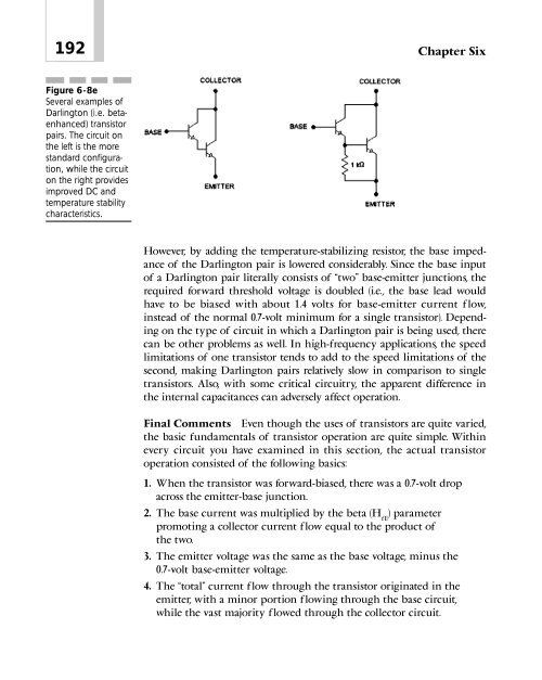
- Page 192 and 193: Transistors (which is the emitter v
- Page 194 and 195: Transistors 175 The transistor circ
- Page 196 and 197: Transistors 177 Again referring to
- Page 198 and 199: Transistors 179 will be very stable
- Page 200 and 201: Transistors 181 Imagine you were go
- Page 202 and 203: Transistors transfer of a voltage s
- Page 204 and 205: Transistors may recall from Chapter
- Page 206 and 207: Transistors 187 base current flow p
- Page 208 and 209: Transistors 189 is connected to its
- Page 212 and 213: Transistors 193 As you have seen, t
- Page 214 and 215: Transistors 195 It might be a littl
- Page 216 and 217: Transistors 197 Figure 6-12 Suggest
- Page 218 and 219: Transistors 199 If a load is placed
- Page 220 and 221: 7 CHAPTER Special-Purpose Diodes an
- Page 222 and 223: Special-Purpose Diodes and Optoelec
- Page 224 and 225: Special-Purpose Diodes and Optoelec
- Page 226 and 227: Special-Purpose Diodes and Optoelec
- Page 228 and 229: Special-Purpose Diodes and Optoelec
- Page 230 and 231: Special-Purpose Diodes and Optoelec
- Page 232 and 233: Special-Purpose Diodes and Optoelec
- Page 234 and 235: Special-Purpose Diodes and Optoelec
- Page 236 and 237: Special-Purpose Diodes and Optoelec
- Page 238 and 239: Special-Purpose Diodes and Optoelec
- Page 240 and 241: Special-Purpose Diodes and Optoelec
- Page 242 and 243: Special-Purpose Diodes and Optoelec
- Page 244 and 245: Special-Purpose Diodes and Optoelec
- Page 246 and 247: + Special-Purpose Diodes and Optoel
- Page 248 and 249: 8 CHAPTER Linear Electronic Circuit
- Page 250 and 251: Linear Electronic Circuits 231 Figu
- Page 252 and 253: Linear Electronic Circuits 233 appl
- Page 254 and 255: Linear Electronic Circuits 235 circ
- Page 256 and 257: Linear Electronic Circuits 237 “a
- Page 258 and 259: Linear Electronic Circuits 239 Dist
- Page 260 and 261:
Linear Electronic Circuits 241 Figu
- Page 262 and 263:
Linear Electronic Circuits 243 To u
- Page 264 and 265:
Linear Electronic Circuits 245 Figu
- Page 266 and 267:
Linear Electronic Circuits 247 Figu
- Page 268 and 269:
Linear Electronic Circuits 249 will
- Page 270 and 271:
Linear Electronic Circuits 251 all
- Page 272 and 273:
Linear Electronic Circuits 253 manu
- Page 274 and 275:
Linear Electronic Circuits 255 minu
- Page 276 and 277:
Linear Electronic Circuits 257 tion
- Page 278 and 279:
Linear Electronic Circuits 259 CAD
- Page 280 and 281:
Linear Electronic Circuits 261 Figu
- Page 282 and 283:
Linear Electronic Circuits 263 Cons
- Page 284 and 285:
Linear Electronic Circuits 265 anyt
- Page 286 and 287:
Linear Electronic Circuits 267 lead
- Page 288 and 289:
Linear Electronic Circuits 269 Note
- Page 290 and 291:
Linear Electronic Circuits 271 Figu
- Page 292 and 293:
Linear Electronic Circuits 273 TABL
- Page 294 and 295:
Linear Electronic Circuits 275 desi
- Page 296 and 297:
Linear Electronic Circuits 277 nal-
- Page 298 and 299:
Linear Electronic Circuits 279 DC).
- Page 300 and 301:
Linear Electronic Circuits 281 ply
- Page 302 and 303:
9 CHAPTER Power Control The term th
- Page 304 and 305:
Power Control 285 matically be reve
- Page 306 and 307:
Power Control equal in both. Theref
- Page 308 and 309:
Power Control 289 V p ) is reached.
- Page 310 and 311:
Power Control 291 There are several
- Page 312 and 313:
Power Control 293 decrease in resis
- Page 314 and 315:
Power Control 295 As explained earl
- Page 316 and 317:
Power Control 297 Figure 9-9 Buffer
- Page 318 and 319:
Power Control 299 Figure 9-10 A sim
- Page 320 and 321:
10 CHAPTER Field-Effect Transistors
- Page 322 and 323:
Field-Effect Transistors 303 Referr
- Page 324 and 325:
Field-Effect Transistors 305 voltag
- Page 326 and 327:
Field-Effect Transistors 307 Static
- Page 328 and 329:
Field-Effect Transistors 309 Figure
- Page 330 and 331:
Field-Effect Transistors 311 functi
- Page 332 and 333:
Field-Effect Transistors 313 Sounds
- Page 334 and 335:
Field-Effect Transistors 315 A UJT
- Page 336 and 337:
11 CHAPTER Batteries Because many h
- Page 338 and 339:
Batteries 319 Gelled electrolyte ba
- Page 340 and 341:
Batteries 321 in which mandatory di
- Page 342 and 343:
Batteries 323 RS1 is set to the pos
- Page 344 and 345:
12 CHAPTER Integrated Circuits The
- Page 346 and 347:
Integrated Circuits 327 mon-mode re
- Page 348 and 349:
Integrated Circuits 329 not be depe
- Page 350 and 351:
Integrated Circuits 331 Improvement
- Page 352 and 353:
Integrated Circuits 333 Figure 12-3
- Page 354 and 355:
Integrated Circuits 335 Figure 12-6
- Page 356 and 357:
Integrated Circuits 337 other filte
- Page 358 and 359:
Integrated Circuits 339 This circui
- Page 360 and 361:
Integrated Circuits 341 connected d
- Page 362 and 363:
13 CHAPTER Digital Electronics Digi
- Page 364 and 365:
Digital Electronics 345 The binary
- Page 366 and 367:
Digital Electronics 347 occur on th
- Page 368 and 369:
Digital Electronics 349 Multivibrat
- Page 370 and 371:
Digital Electronics 351 F-F1 will t
- Page 372 and 373:
Digital Electronics 353 Figure 13-6
- Page 374 and 375:
Digital Electronics 355 Summary Man
- Page 376 and 377:
Digital Electronics 357 IC2 is a CM
- Page 378 and 379:
Digital Electronics 359 Figure 13-1
- Page 380 and 381:
14 CHAPTER Computers In today’s w
- Page 382 and 383:
Computers 363 Figure 14-1 Block dia
- Page 384 and 385:
Computers 365 memory. Then, during
- Page 386 and 387:
Computers 367 When an I/O port “s
- Page 388 and 389:
Computers 369 with real analysis eq
- Page 390 and 391:
15 CHAPTER More About Capacitors an
- Page 392 and 393:
More About Capacitors and Inductors
- Page 394 and 395:
More About Capacitors and Inductors
- Page 396 and 397:
More About Capacitors and Inductors
- Page 398 and 399:
More About Capacitors and Inductors
- Page 400 and 401:
More About Capacitors and Inductors
- Page 402 and 403:
More About Capacitors and Inductors
- Page 404 and 405:
More About Capacitors and Inductors
- Page 406 and 407:
More About Capacitors and Inductors
- Page 408 and 409:
More About Capacitors and Inductors
- Page 410 and 411:
More About Capacitors and Inductors
- Page 412 and 413:
More About Capacitors and Inductors
- Page 414 and 415:
More About Capacitors and Inductors
- Page 416 and 417:
More About Capacitors and Inductors
- Page 418 and 419:
More About Capacitors and Inductors
- Page 420 and 421:
More About Capacitors and Inductors
- Page 422 and 423:
More About Capacitors and Inductors
- Page 424 and 425:
16 CHAPTER Radio and Television Rad
- Page 426 and 427:
Radio and Television 407 Figure 16-
- Page 428 and 429:
Radio and Television 409 length. At
- Page 430 and 431:
Radio and Television 411 the RF spe
- Page 432 and 433:
Radio and Television 413 tude varia
- Page 434 and 435:
Radio and Television 415 Figure 16-
- Page 436 and 437:
APPENDIX A SYMBOLS AND EQUATIONS Th
- Page 438 and 439:
Symbols and Equations 419 IF Interm
- Page 440 and 441:
Symbols and Equations 421 rcvr Rece
- Page 442 and 443:
Symbols and Equations 423 Formulas
- Page 444 and 445:
Symbols and Equations 425 I 20 log
- Page 446 and 447:
Symbols and Equations Meter formula
- Page 448 and 449:
Symbols and Equations 429 Resistanc
- Page 450:
Symbols and Equations 431 Temperatu
- Page 453 and 454:
434 Appendix B Electronic Kit Suppl
- Page 455 and 456:
436 Appendix B Marlin P. Jones & As
- Page 457 and 458:
This page intentionally left blank.
- Page 459 and 460:
440 Appendix C Figure C-1 (cont.) 1
- Page 461 and 462:
This page intentionally left blank.
- Page 463 and 464:
444 Index Amplifiers, audio (Cont.)
- Page 465 and 466:
446 Index Capacitance and capacitor
- Page 467 and 468:
448 Index Digital ICs, 326 Digital
- Page 469 and 470:
450 Index Filters (Cont.): Percussi
- Page 471 and 472:
452 Index Lab for electronics work,
- Page 473 and 474:
454 Index Photographic method for p
- Page 475 and 476:
456 Index Resist ink in printed cir
- Page 477 and 478:
458 Index Transformers (Cont.): Iso
- Page 479:
ABOUT THE AUTHOR G. Randy Slone is