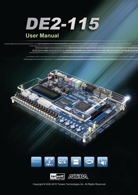
DE2-115: User Manual
DE2-115: User Manual
DE2-115: User Manual

Create successful ePaper yourself
Turn your PDF publications into a flip-book with our unique Google optimized e-Paper software.
CONTENTS<br />
Chapter 1 <strong>DE2</strong>-<strong>115</strong> Package .................................................................................. 4<br />
1.1 Package Contents .................................................................................................................................. 4<br />
1.2 The <strong>DE2</strong>-<strong>115</strong> Board Assembly .............................................................................................................. 5<br />
1.3 Getting Help ......................................................................................................................................... 6<br />
Chapter 2 Introduction of the Altera <strong>DE2</strong>-<strong>115</strong> Board ............................................ 7<br />
2.1 Layout and Components ........................................................................................................................ 7<br />
2.2 Block Diagram of the <strong>DE2</strong>-<strong>115</strong> Board ................................................................................................... 9<br />
2.3 Power-up the <strong>DE2</strong>-<strong>115</strong> Board .............................................................................................................. 12<br />
Chapter 3 <strong>DE2</strong>-<strong>115</strong> Control Panel ........................................................................ 14<br />
3.1 Control Panel Setup ............................................................................................................................ 14<br />
3.2 Controlling the LEDs, 7-segment Displays and LCD Display............................................................ 16<br />
3.3 Switches and Push-buttons .................................................................................................................. 18<br />
3.4 SDRAM/SRAM/EEPROM/Flash Controller and Program-mer ........................................................... 19<br />
3.5 USB Monitoring ................................................................................................................................. 21<br />
3.6 PS/2 Device ........................................................................................................................................ 22<br />
3.7 SD Card .............................................................................................................................................. 23<br />
3.8 RS-232 Communication ...................................................................................................................... 23<br />
3.9 VGA ................................................................................................................................................... 24<br />
3.10 HSMC .............................................................................................................................................. 25<br />
3.11 IR Receiver ....................................................................................................................................... 26<br />
3.12 Overall Structure of the <strong>DE2</strong>-<strong>115</strong> Control Panel ................................................................................ 27<br />
Chapter 4 Using the <strong>DE2</strong>-<strong>115</strong> Board .................................................................... 29<br />
4.1 Configuring the Cyclone IV E FPGA .................................................................................................. 29<br />
4.2 Using Push-buttons and Switches ........................................................................................................ 32<br />
1
4.3 Using LEDs ........................................................................................................................................ 34<br />
4.4 Using the 7-segment Displays ............................................................................................................. 36<br />
4.5 Clock Circuitry ................................................................................................................................... 38<br />
4.6 Using the LCD Module ....................................................................................................................... 39<br />
4.7 High Speed Mezzanine Card ............................................................................................................... 40<br />
4.8 Using the Expansion Header ............................................................................................................... 45<br />
4.9 Using 14-pin General Purpose I/O Connector ...................................................................................... 50<br />
4.10 Using VGA ....................................................................................................................................... 51<br />
4.11 Using the 24-bit Audio CODEC ........................................................................................................ 53<br />
4.12 RS-232 Serial Port ............................................................................................................................ 54<br />
4.13 PS/2 Serial Port ................................................................................................................................. 55<br />
4.14 Gigabit Ethernet Transceiver ............................................................................................................. 56<br />
4.15 TV Decoder ...................................................................................................................................... 59<br />
4.16 Implementing a TV Encoder.............................................................................................................. 60<br />
4.17 Using the USB Interface .................................................................................................................... 61<br />
4.18 Using IR ........................................................................................................................................... 62<br />
4.19 Using SRAM/SDRAM/FLASH/EEPROM/SD Card .......................................................................... 63<br />
Chapter 5 <strong>DE2</strong>-<strong>115</strong> System Builder ..................................................................... 70<br />
5.1 Introduction ........................................................................................................................................ 70<br />
5.2 General Design Flow .......................................................................................................................... 70<br />
5.3 Using <strong>DE2</strong>-<strong>115</strong> System Builder ........................................................................................................... 71<br />
Chapter 6 Examples of Advanced Demonstrations ............................................. 77<br />
6.1 <strong>DE2</strong>-<strong>115</strong> Factory Configuration .......................................................................................................... 77<br />
6.2 TV Box Demonstration ....................................................................................................................... 78<br />
6.3 USB Paintbrush .................................................................................................................................. 80<br />
6.4 USB Device ........................................................................................................................................ 82<br />
6.5 A Karaoke Machine ............................................................................................................................. 84<br />
6.6 SD Card Demonstration ...................................................................................................................... 86<br />
6.7 SD Card Music Player ......................................................................................................................... 89<br />
6.8 PS/2 Mouse Demonstration ................................................................................................................. 93<br />
2
6.9 IR Receiver Demonstration ................................................................................................................. 96<br />
6.10 Music Synthesizer Demonstration ................................................................................................... 100<br />
6.11 Audio Recording and Playing .......................................................................................................... 103<br />
6.12 Web Server Demonstration .............................................................................................................. 106<br />
Chapter 7 Appendix .......................................................................................... <strong>115</strong><br />
7.1 Revision History ............................................................................................................................... <strong>115</strong><br />
7.2 Copyright Statement.......................................................................................................................... <strong>115</strong><br />
3
Chapter 1<br />
<strong>DE2</strong>-<strong>115</strong> Package<br />
The <strong>DE2</strong>-<strong>115</strong> package contains all components needed to use the <strong>DE2</strong>-<strong>115</strong> board in conjunction<br />
with a computer that runs the Microsoft Windows OS.<br />
1.1 Package Contents<br />
Figure 1-1 shows a photograph of the <strong>DE2</strong>-<strong>115</strong> package.<br />
Figure 1-1 The <strong>DE2</strong>-<strong>115</strong> package contents<br />
The <strong>DE2</strong>-<strong>115</strong> package includes:<br />
The <strong>DE2</strong>-<strong>115</strong> board.<br />
USB Cable for FPGA programming and control.<br />
<strong>DE2</strong>-<strong>115</strong> System CD containing the <strong>DE2</strong>-<strong>115</strong> documentation and supporting materials,<br />
including the <strong>User</strong> <strong>Manual</strong>, the Control Panel, System Builder and Altera Monitor Program<br />
utility, reference designs and demonstrations, device datasheets, tutorials, and a set of laboratory<br />
exercises.<br />
CD-ROMs containing Altera‟s Quartus® II Web Edition and the Nios® II Embedded Design<br />
Suit Evaluation Edition software.<br />
4
Bag of six rubber (silicon) covers for the <strong>DE2</strong>-<strong>115</strong> board stands. The bag also contains some<br />
extender pins, which can be used to facilitate easier probing with testing equipment of the<br />
board‟s I/O expansion headers.<br />
Clear plastic cover for the board.<br />
12V DC desktop power supply.<br />
Remote controller<br />
1.2 The <strong>DE2</strong>-<strong>115</strong> Board Assembly<br />
To assemble the included stands for the <strong>DE2</strong>-<strong>115</strong> board:<br />
Assemble a rubber (silicon) cover, as shown in Figure 1-2, for each of the six copper stands on<br />
the <strong>DE2</strong>-<strong>115</strong> board<br />
The clear plastic cover provides extra protection, and is mounted over the top of the board by<br />
using additional stands and screws<br />
Figure 1-2 The feet for the <strong>DE2</strong>-<strong>115</strong> board<br />
5
1.3 Getting Help<br />
Here are the addresses where you can get help if you encounter any problem:<br />
Altera Corporation<br />
101 Innovation Drive San Jose, California, 95134 USA<br />
Email: university@altera.com<br />
Terasic Technologies<br />
No. 356, Sec. 1, Fusing E. Rd. Jhubei City, HsinChu County, Taiwan, 302<br />
Email: support@terasic.com<br />
Tel.: +886-3-550-8800<br />
Web: <strong>DE2</strong>-<strong>115</strong>.terasic.com<br />
6
Chapter 2<br />
Introduction of the Altera <strong>DE2</strong>-<strong>115</strong> Board<br />
This chapter presents the features and design characteristics of the <strong>DE2</strong>-<strong>115</strong> board.<br />
2.1 Layout and Components<br />
A photograph of the <strong>DE2</strong>-<strong>115</strong> board is shown in Figure 2-1 and Figure 2-2. It depicts the layout of<br />
the board and indicates the location of the connectors and key components.<br />
Figure 2-1 The <strong>DE2</strong>-<strong>115</strong> board (top view)<br />
7
Figure 2-2 The <strong>DE2</strong>-<strong>115</strong> board (bottom view)<br />
The <strong>DE2</strong>-<strong>115</strong> board has many features that allow users to implement a wide range of designed<br />
circuits, from simple circuits to various multimedia projects.<br />
The following hardware is provided on the <strong>DE2</strong>-<strong>115</strong> board:<br />
Altera Cyclone® IV 4CE<strong>115</strong> FPGA device<br />
Altera Serial Configuration device – EPCS64<br />
USB Blaster (on board) for programming; both JTAG and Active Serial (AS) programming<br />
modes are supported<br />
2MB SRAM<br />
Two 64MB SDRAM<br />
8MB Flash memory<br />
SD Card socket<br />
4 Push-buttons<br />
18 Slide switches<br />
18 Red user LEDs<br />
9 Green user LEDs<br />
50MHz oscillator for clock sources<br />
24-bit CD-quality audio CODEC with line-in, line-out, and microphone-in jacks<br />
VGA DAC (8-bit high-speed triple DACs) with VGA-out connector<br />
TV Decoder (NTSC/PAL/SECAM) and TV-in connector<br />
2 Gigabit Ethernet PHY with RJ45 connectors<br />
USB Host/Slave Controller with USB type A and type B connectors<br />
RS-232 transceiver and 9-pin connector<br />
PS/2 mouse/keyboard connector<br />
IR Receiver<br />
2 SMA connectors for external clock input/output<br />
8
One 40-pin Expansion Header with diode protection<br />
One High Speed Mezzanine Card (HSMC) connector<br />
16x2 LCD module<br />
In addition to these hardware features, the <strong>DE2</strong>-<strong>115</strong> board has software support for standard I/O<br />
interfaces and a control panel facility for accessing various components. Also, the software is<br />
provided for supporting a number of demonstrations that illustrate the advanced capabilities of the<br />
<strong>DE2</strong>-<strong>115</strong> board.<br />
In order to use the <strong>DE2</strong>-<strong>115</strong> board, the user has to be familiar with the Quartus II software. The<br />
necessary knowledge can be acquired by reading the tutorials “Getting Started with Altera’s <strong>DE2</strong>-<strong>115</strong><br />
Board” (tut_initial<strong>DE2</strong>-<strong>115</strong>.pdf) and “Quartus II Introduction” (which exists in three versions based on the design<br />
entry method used, namely Verilog, VHDL or schematic entry). These tutorials are provided in the directory<br />
<strong>DE2</strong>_<strong>115</strong>_tutorials on the <strong>DE2</strong>-<strong>115</strong> System CD that accompanies the <strong>DE2</strong>-<strong>115</strong> kit and can also be found on<br />
Terasic‟s <strong>DE2</strong>-<strong>115</strong> web pages.<br />
2.2 Block Diagram of the <strong>DE2</strong>-<strong>115</strong> Board<br />
Figure 2-3 gives the block diagram of the <strong>DE2</strong>-<strong>115</strong> board. To provide maximum flexibility for the<br />
user, all connections are made through the Cyclone IV E FPGA device. Thus, the user can configure<br />
the FPGA to implement any system design.<br />
Figure 2-3 Block Diagram of <strong>DE2</strong>-<strong>115</strong><br />
9
Following is more detailed information about the blocks in Figure 2-3:<br />
FPGA device<br />
Cyclone IV EP4CE<strong>115</strong>F29 device<br />
114,480 LEs<br />
432 M9K memory blocks<br />
3,888 Kbits embedded memory<br />
4 PLLs<br />
FPGA configuration<br />
JTAG and AS mode configuration<br />
EPCS64 serial configuration device<br />
On-board USB Blaster circuitry<br />
Memory devices<br />
128MB (32Mx32bit) SDRAM<br />
2MB (1Mx16) SRAM<br />
8MB (4Mx16) Flash with 8-bit mode<br />
32Kb EEPROM<br />
SD Card socket<br />
Provides SPI and 4-bit SD mode for SD Card access<br />
Connectors<br />
Two Ethernet 10/100/1000 Mbps ports<br />
High Speed Mezzanine Card (HSMC)<br />
Configurable I/O standards (voltage levels:3.3/2.5/1.8/1.5V)<br />
USB type A and B<br />
o Provide host and device controllers compliant with USB 2.0<br />
o Support data transfer at full-speed and low-speed<br />
o PC driver available<br />
10
40-pin expansion port<br />
o Configurable I/O standards (voltage levels:3.3/2.5/1.8/1.5V)<br />
VGA-out connector<br />
o VGA DAC (high speed triple DACs)<br />
DB9 serial connector for RS-232 port with flow control<br />
PS/2 mouse/keyboard<br />
Clock<br />
Three 50MHz oscillator clock inputs<br />
SMA connectors (external clock input/output)<br />
Audio<br />
24-bit encoder/decoder (CODEC)<br />
Line-in, line-out, and microphone-in jacks<br />
Display<br />
16x2 LCD module<br />
Switches and indicators<br />
18 slide switches and 4 push-buttons switches<br />
18 red and 9 green LEDs<br />
Eight 7-segment displays<br />
Other features<br />
Infrared remote-control receiver module<br />
TV decoder (NTSC/PAL/SECAM) and TV-in connector<br />
11
Power<br />
Desktop DC input<br />
Switching and step-down regulators LM3150MH<br />
2.3 Power-up the <strong>DE2</strong>-<strong>115</strong> Board<br />
The <strong>DE2</strong>-<strong>115</strong> board comes with a preloaded configuration bit stream to demonstrate some features<br />
of the board. This bit stream also allows users to see quickly if the board is working properly. To<br />
power-up the board perform the following steps:<br />
1. Connect the provided USB cable from the host computer to the USB Blaster connector on the<br />
<strong>DE2</strong>-<strong>115</strong> board. For communication between the host and the <strong>DE2</strong>-<strong>115</strong> board, it is necessary<br />
to install the Altera USB Blaster driver software. If this driver is not already installed on the<br />
host computer, it can be installed as explained in the tutorial “Getting Started with Altera's<br />
<strong>DE2</strong>-<strong>115</strong> Board ” (tut_initial<strong>DE2</strong>-<strong>115</strong>.pdf). This tutorial is available in the directory<br />
<strong>DE2</strong>_<strong>115</strong>_tutorials on the <strong>DE2</strong>-<strong>115</strong> System CD.<br />
2. Turn off the power by pressing the red ON/OFF switch before connecting the 12V adapter to<br />
the <strong>DE2</strong>-<strong>115</strong> board.<br />
3. Connect a VGA monitor to the VGA port on the <strong>DE2</strong>-<strong>115</strong> board.<br />
4. Connect your headset to the line-out audio port on the <strong>DE2</strong>-<strong>115</strong> board.<br />
5. Turn the RUN/PROG switch (SW19) on the left edge of the <strong>DE2</strong>-<strong>115</strong> board to RUN position;<br />
the PROG position is used only for the AS Mode programming.<br />
6. Recycle the power by turning the red power switch on the <strong>DE2</strong>-<strong>115</strong> board OFF and ON again .<br />
At this point you should observe the following:<br />
All user LEDs are flashing<br />
All 7-segment displays are cycling through the numbers 0 to F<br />
The LCD display shows “Welcome to the Altera <strong>DE2</strong>-<strong>115</strong>”<br />
The VGA monitor displays the image shown in Figure 2-4<br />
Set the slide switch SW17 to the DOWN position; you should hear a 1-kHz sound. Be careful of<br />
the very loud volume for avoiding any discomfort<br />
Set the slide switch SW17 to the UP position and connect the output of an audio player to the<br />
line-in connector on the <strong>DE2</strong>-<strong>115</strong> board; on your speaker or headset you should hear the music<br />
played from the audio player (MP3, PC, iPod, or the like)<br />
12
You can also connect a microphone to the microphone-in connector on the <strong>DE2</strong>-<strong>115</strong> board; your<br />
voice will be mixed with the music playing on the audio player<br />
Figure 2-4 The default VGA output pattern<br />
13
Chapter 3<br />
<strong>DE2</strong>-<strong>115</strong> Control Panel<br />
The <strong>DE2</strong>-<strong>115</strong> board comes with a Control Panel facility that allows users to access various<br />
components on the board from a host computer. The host computer communicates with the board<br />
through a USB connection. The facility can be used to verify the functionality of components on the<br />
board or be used as a debug tool while developing RTL code.<br />
This chapter first presents some basic functions of the Control Panel, then describes its structure in<br />
block diagram form, and finally describes its capabilities.<br />
3.1 Control Panel Setup<br />
The Control Panel Software Utility is located in the directory<br />
“<strong>DE2</strong>_<strong>115</strong>_tools/<strong>DE2</strong>_<strong>115</strong>_control_panel” in the <strong>DE2</strong>-<strong>115</strong> System CD. It's free of installation, just<br />
copy the whole folder to your host computer and launch the control panel by executing the<br />
“<strong>DE2</strong>_<strong>115</strong>_ControlPanel.exe”. (Windows 7 64-bit <strong>User</strong>s: If an error message that shows a missing<br />
jtag_client.dll file (cannot find jtag_client.dll) while the Control Panel is commencing, users should<br />
re-launch the DE4_ControlPanel.exe from the following directory<br />
(/<strong>DE2</strong>_<strong>115</strong>_tools/<strong>DE2</strong>_<strong>115</strong>_control_panel/win7_64bits))<br />
Specific control circuit should be downloaded to your FPGA board before the control panel can<br />
request it to perform required tasks. The program will call Quartus II tools to download the control<br />
circuit to the FPGA board through USB-Blaster[USB-0] connection.<br />
To activate the Control Panel, perform the following steps:<br />
1. Make sure Quartus II 10.0 or later version is installed successfully on your PC.<br />
2. Set the RUN/PROG switch to the RUN position.<br />
3. Connect the supplied USB cable to the USB Blaster port, connect the 12V power supply, and<br />
turn the power switch ON.<br />
4. Start the executable <strong>DE2</strong>_<strong>115</strong>_ControlPanel.exe on the host computer. The Control Panel user<br />
interface shown in Figure 3-1 will appear.<br />
14
5. The <strong>DE2</strong>_<strong>115</strong>_ControlPanel.sof bit stream is loaded automatically as soon as the<br />
<strong>DE2</strong>_<strong>115</strong>_control_panel.exe is launched.<br />
6. In case the connection is disconnected, click on CONNECT where the .sof will be re-loaded<br />
onto the board.<br />
7. Note, the Control Panel will occupy the USB port until you close that port; you cannot use Quartus II to<br />
download a configuration file into the FPGA until the USB port is closed.<br />
8. The Control Panel is now ready for use; experience it by setting the ON/OFF status for some<br />
LEDs and observing the result on the <strong>DE2</strong>-<strong>115</strong> board.<br />
Figure 3-1 The <strong>DE2</strong>-<strong>115</strong> Control Panel<br />
The concept of the <strong>DE2</strong>-<strong>115</strong> Control Panel is illustrated in Figure 3-2. The “Control Circuit” that<br />
performs the control functions is implemented in the FPGA board. It communicates with the<br />
Control Panel window, which is active on the host computer, via the USB Blaster link. The<br />
graphical interface is used to issue commands to the control circuit. It handles all requests and<br />
performs data transfers between the computer and the <strong>DE2</strong>-<strong>115</strong> board.<br />
15
Figure 3-2 The <strong>DE2</strong>-<strong>115</strong> Control Panel concept<br />
The <strong>DE2</strong>-<strong>115</strong> Control Panel can be used to light up LEDs, change the values displayed on<br />
7-segment and LCD displays, monitor buttons/switches status, read/write the SDRAM, SRAM,<br />
EEPROM and Flash Memory, monitor the status of an USB device, communicate with the PS/2<br />
mouse, output VGA color pattern to VGA monitor, verify functionality of HSMC connector I/Os,<br />
communicate with PC via RS-232 interface and read SD Card specification information. The<br />
feature of reading/writing a word or an entire file from/to the Flash Memory allows the user to<br />
develop multimedia applications (Flash Audio Player, Flash Picture Viewer) without worrying about<br />
how to build a Memory Programmer.<br />
3.2 Controlling the LEDs, 7-segment Displays and LCD<br />
Display<br />
A simple function of the Control Panel is to allow setting the values displayed on LEDs, 7-segment<br />
displays, and the LCD character display.<br />
Choosing the LED tab leads to the window in Figure 3-3. Here, you can directly turn the LEDs on<br />
or off individually or by clicking “Light All” or “Unlight All”.<br />
16
Figure 3-3 Controlling LEDs<br />
Choosing the 7-SEG tab leads to the window shown in Figure 3-4. From the window, directly use<br />
the left-right arrows to control the 7-SEG patterns on the <strong>DE2</strong>-<strong>115</strong> board which are updated<br />
immediately. Note that the dots of the 7-SEGs are not enabled on <strong>DE2</strong>-<strong>115</strong> board.<br />
Figure 3-4 Controlling 7-SEG display<br />
17
Choosing the LCD tab leads to the window in Figure 3-5. Text can be written to the LCD display<br />
by typing it in the LCD box then pressing the Set button.<br />
Figure 3-5 Controlling the LCD display<br />
The ability to set arbitrary values into simple display devices is not needed in typical design<br />
activities. However, it gives the user a simple mechanism for verifying that these devices are<br />
functioning correctly in case a malfunction is suspected. Thus, it can be used for troubleshooting<br />
purposes.<br />
3.3 Switches and Push-buttons<br />
Choosing the Switches tab leads to the window in Figure 3-6. The function is designed to monitor<br />
the status of slide switches and push-buttons in real time and show the status in a graphical user<br />
interface. It can be used to verify the functionality of the slide switches and push-buttons.<br />
18
Figure 3-6 Monitoring switches and buttons<br />
The ability to check the status of push-button and slide switch is not needed in typical design<br />
activities. However, it provides users a simple mechanism for verifying if the buttons and switches<br />
are functioning correctly. Thus, it can be used for troubleshooting purposes.<br />
3.4 SDRAM/SRAM/EEPROM/Flash Controller and Programmer<br />
The Control Panel can be used to write/read data to/from the SDRAM, SRAM, EEPROM, and<br />
Flash chips on the <strong>DE2</strong>-<strong>115</strong> board. As an example, we will describe how the SDRAM may be<br />
accessed; the same approach is used to access the SRAM, EEPROM, and Flash. Click on the<br />
Memory tab and select “SDRAM” to reach the window in Figure 3-7.<br />
19
Figure 3-7 Accessing the SDRAM<br />
A 16-bit word can be written into the SDRAM by entering the address of the desired location,<br />
specifying the data to be written, and pressing the Write button. Contents of the location can be read<br />
by pressing the Read button. Figure 3-7 depicts the result of writing the hexadecimal value 06CA<br />
into offset address 200, followed by reading the same location.<br />
The Sequential Write function of the Control Panel is used to write the contents of a file into the<br />
SDRAM as follows:<br />
1. Specify the starting address in the Address box.<br />
2. Specify the number of bytes to be written in the Length box. If the entire file is to be loaded,<br />
then a checkmark may be placed in the File Length box instead of giving the number of bytes.<br />
3. To initiate the writing process, click on the Write a File to Memory button.<br />
4. When the Control Panel responds with the standard Windows dialog box asking for the source<br />
file, specify the desired file in the usual manner.<br />
The Control Panel also supports loading files with a .hex extension. Files with a .hex extension are<br />
ASCII text files that specify memory values using ASCII characters to represent hexadecimal<br />
values. For example, a file containing the line<br />
0123456789ABCDEF<br />
Defines eight 8-bit values: 01, 23, 45, 67, 89, AB, CD, EF. These values will be loaded<br />
consecutively into the memory.<br />
20
The Sequential Read function is used to read the contents of the SDRAM and fill them into a file as<br />
follows:<br />
1. Specify the starting address in the Address box.<br />
2. Specify the number of bytes to be copied into the file in the Length box. If the entire contents<br />
of the SDRAM are to be copied (which involves all 128 Mbytes), then place a checkmark in<br />
the Entire Memory box.<br />
3. Press Load Memory Content to a File button.<br />
4. When the Control Panel responds with the standard Windows dialog box asking for the<br />
destination file, specify the desired file in the usual manner.<br />
<strong>User</strong>s can use the similar way to access the SRAM, EEPROM and Flash. Please note that users<br />
need to erase the Flash before writing data to it.<br />
3.5 USB Monitoring<br />
The Control Panel provides users a USB monitoring tool which monitors the status of the USB<br />
devices connected to the USB port on the <strong>DE2</strong>-<strong>115</strong> board. By plugging in a USB device to the USB<br />
host port of the board, the device type is displayed on the control window. Figure 3-8 shows a USB<br />
mouse plugged into the host USB port.<br />
Figure 3-8 USB Mouse Monitoring Tool<br />
21
3.6 PS/2 Device<br />
The Control Panel provides users a PS/2 monitoring tool which monitors the real-time status of a<br />
PS/2 mouse connected to the <strong>DE2</strong>-<strong>115</strong> board. The movement of the mouse and the status of the<br />
three buttons will be shown in the graphical and text interface. The mouse movement is translated<br />
as a position (x,y) with range from (0,0)~(1023,767). This function can be used to verify the<br />
functionality of the PS/2 connection.<br />
Follow the steps below to exercise the PS/2 Mouse Monitoring tool:<br />
1. Choosing the PS/2 tab leads to the window in Figure 3-9.<br />
2. Plug a PS/2 mouse to the PS/2 port on the <strong>DE2</strong>-<strong>115</strong> board.<br />
3. Press the Start button to start the PS/2 mouse monitoring process, and the button caption is<br />
changed from Start to Stop. In the monitoring process, the status of the PS/2 mouse is updated<br />
and shown in the Control Panel‟s GUI window in real-time. Press Stop to terminate the<br />
monitoring process.<br />
Figure 3-9 PS/2 Mouse Monitoring Tool<br />
22
3.7 SD Card<br />
The function is designed to read the identification and specification information of the SD Card.<br />
The 4-bit SD MODE is used to access the SD Card. This function can be used to verify the<br />
functionality of the SD Card Interface. Follow the steps below to exercise the SD Card:<br />
1. Choosing the SD Card tab leads to the window in Figure 3-10.<br />
2. Insert an SD Card to the <strong>DE2</strong>-<strong>115</strong> board, and then press the Read button to read the SD Card.<br />
The SD Card‟s identification, specification, and file format information will be displayed in the<br />
control window.<br />
Figure 3-10 Reading the SD Card Identification and Specification<br />
3.8 RS-232 Communication<br />
The Control Panel allows users to verify the operation of the RS-232 serial communication interface<br />
on the <strong>DE2</strong>-<strong>115</strong>. The setup is established by connecting a RS-232 9-pin male to female cable from<br />
the PC to the RS-232 port where the Control Panel communicates to the terminal emulator software<br />
on the PC, or vice versa. Alternatively, a RS-232 loopback cable can also be used if you do not wish<br />
to use the PC to verify the test. The Receive terminal window on the Control Panel monitors the<br />
serial communication status. Follow the steps below to initiate the RS-232 communication:<br />
23
1. Choosing the RS-232 tab leads to the window in Figure 3-11.<br />
2. Plug in a RS-232 9-pin male to female cable from PC to RS-232 port or a RS-232 loopback<br />
cable directly to RS-232 port.<br />
3. The RS-232 settings are provided below in case a connection from the PC is used:<br />
Baud Rate: <strong>115</strong>200<br />
Parity Check Bit: None<br />
Data Bits: 8<br />
Stop Bits: 1<br />
Flow Control (CTS/RTS): ON<br />
4. To begin the communication, enter specific letters followed by clicking Send. During the<br />
communication process, observe the status of the Receive terminal window to verify its<br />
operation.<br />
Figure 3-11 RS-232 Serial Communication<br />
3.9 VGA<br />
<strong>DE2</strong>-<strong>115</strong> Control Panel provides VGA pattern function that allows users to output color pattern to<br />
LCD/CRT monitor using the <strong>DE2</strong>-<strong>115</strong> board. Follow the steps below to generate the VGA pattern<br />
function:<br />
24
1. Choosing the VGA tab leads to the window in Figure 3-12.<br />
2. Plug a D-sub cable to VGA connector of the <strong>DE2</strong>-<strong>115</strong> board and LCD/CRT monitor.<br />
3. The LCD/CRT monitor will display the same color pattern on the control panel window.<br />
4. Click the drop down menu shown in Figure 3-12 where you can output the selected color<br />
individually.<br />
Figure 3-12 Controlling VGA display<br />
3.10 HSMC<br />
Select the HSMC tab to reach the window shown in Figure 3-13. This function is designed to verify<br />
the functionality of the signals located on the HSMC connector. Before running the HSMC<br />
loopback verification test, follow the instruction noted under the Loopback Installation section and<br />
click on Verify. Please note to turn off the <strong>DE2</strong>-<strong>115</strong> board before the HSMC loopback adapter is<br />
installed to prevent any damage to the board.<br />
The HSMC loopback adapter is not provided in the kit package but can be purchased through the<br />
website below:<br />
(http://www.terasic.com.tw/cgi-bin/page/archive.pl?Language=English&CategoryNo=78&No=495)<br />
25
Figure 3-13 HSMC loopback verification test performed under Control Panel<br />
3.11 IR Receiver<br />
From the control panel, we can test the IR receiver on the <strong>DE2</strong>-<strong>115</strong> by sending scan code from a<br />
remote controller. Figure 3-14 depicts the IR receiver window when the IR tab is pressed. When the<br />
scan code is received, the information will be displayed on the IR Receiver window represented in<br />
hexadecimal. Also, the pressed button on the remote controller will be indicated on the graphic of<br />
remote controller on the IR receiver window. Note that there exists several encoding form among<br />
different brands of remote controllers. Only the remote controller comes with the kit is confirmed to<br />
be compatible with this software.<br />
26
Figure 3-14 Testing the IR receiver using remote controller<br />
3.12 Overall Structure of the <strong>DE2</strong>-<strong>115</strong> Control Panel<br />
The <strong>DE2</strong>-<strong>115</strong> Control Panel is based on a Nios II SOPC system instantiated in the Cyclone IV E<br />
FPGA with software running on the on-chip memory. The software part is implemented in C code;<br />
the hardware part is implemented in Verilog HDL code with SOPC builder. The source code is not<br />
available on the <strong>DE2</strong>_<strong>115</strong> System CD.<br />
To run the Control Panel, users should make the configuration according to Section 3.1. Figure<br />
3-15 depicts the structure of the Control Panel. Each input/output device is controlled by the Nios II<br />
Processor instantiated in the FPGA chip. The communication with the PC is done via the USB<br />
Blaster link. The Nios II interprets the commands sent from the PC and performs the corresponding<br />
actions.<br />
27
Figure 3-15 The block diagram of the <strong>DE2</strong>-<strong>115</strong> control panel<br />
28
Chapter 4<br />
Using the <strong>DE2</strong>-<strong>115</strong> Board<br />
This chapter gives instructions for using the <strong>DE2</strong>-<strong>115</strong> board and describes each of its peripherals.<br />
4.1 Configuring the Cyclone IV E FPGA<br />
The procedure for downloading a circuit from a host computer to the <strong>DE2</strong>-<strong>115</strong> board is described in<br />
the tutorial Quartus II Introduction. This tutorial is found in the <strong>DE2</strong>_<strong>115</strong>_tutorials folder on the<br />
<strong>DE2</strong>-<strong>115</strong> System CD. The user is encouraged to read the tutorial first, and treat the information<br />
below as a short reference.<br />
The <strong>DE2</strong>-<strong>115</strong> board contains a serial configuration device that stores configuration data for the<br />
Cyclone IV E FPGA. This configuration data is automatically loaded from the configuration device<br />
into the FPGA every time while power is applied to the board. Using the Quartus II software, it is<br />
possible to reconfigure the FPGA at any time, and it is also possible to change the non-volatile data<br />
that is stored in the serial configuration device. Both types of programming methods are described<br />
below.<br />
1. JTAG programming: In this method of programming, named after the IEEE standards Joint<br />
Test Action Group, the configuration bit stream is downloaded directly into the Cyclone IV E<br />
FPGA. The FPGA will retain this configuration as long as power is applied to the board; the<br />
configuration information will be lost when the power is turned off.<br />
2. AS programming: In this method, called Active Serial programming, the configuration bit<br />
stream is downloaded into the Altera EPCS64 serial configuration device. It provides<br />
non-volatile storage of the bit stream, so that the information is retained even when the power<br />
supply to the <strong>DE2</strong>-<strong>115</strong> board is turned off. When the board‟s power is turned on, the<br />
configuration data in the EPCS64 device is automatically loaded into the Cyclone IV E FPGA.<br />
• JTAG Chain on <strong>DE2</strong>-<strong>115</strong> Board<br />
To use JTAG interface for configuring FPGA device, the JTAG chain on <strong>DE2</strong>-<strong>115</strong> must form a<br />
close loop that allows Quartus II programmer to detect FPGA device. Figure 4-1 illustrates the<br />
JTAG chain on <strong>DE2</strong>-<strong>115</strong> board. Shorting pin1 and pin2 on JP3 can disable the JTAG signals on<br />
29
HSMC connector that will form a close JTAG loop chain on <strong>DE2</strong>-<strong>115</strong> board (See Figure 4-2). Thus,<br />
only the on board FPGA device (Cyclone IV E) will be detected by Quartus II programmer. If users<br />
want to include another FPGA device or interface containing FPGA device in the chain via HSMC<br />
connector, short pin2 and pin3 on JP3 to enable the JTAG signal ports on the HSMC connector.<br />
Figure 4-1 The JTAG chain on <strong>DE2</strong>-<strong>115</strong> board<br />
Figure 4-2 The JTAG chain configuration header<br />
The sections below describe the steps used to perform both JTAG and AS programming. For both<br />
methods the <strong>DE2</strong>-<strong>115</strong> board is connected to a host computer via a USB cable. Using this connection,<br />
the board will be identified by the host computer as an Altera USB Blaster device. The process for<br />
installing on the host computer the necessary software device driver that communicates with the<br />
USB Blaster is described in the tutorial “Getting Started with Altera’s <strong>DE2</strong>-<strong>115</strong> Board”<br />
(tut_initial<strong>DE2</strong>-<strong>115</strong>.pdf). This tutorial is available on the <strong>DE2</strong>-<strong>115</strong> System CD.<br />
30
• Configuring the FPGA in JTAG Mode<br />
Figure 4-3 illustrates the JTAG configuration setup. To download a configuration bit stream into<br />
the Cyclone IV E FPGA, perform the following steps:<br />
Ensure that power is applied to the <strong>DE2</strong>-<strong>115</strong> board<br />
Configure the JTAG programming circuit by setting the RUN/PROG slide switch (SW19) to the<br />
RUN position (See Figure 4-4)<br />
Connect the supplied USB cable to the USB Blaster port on the <strong>DE2</strong>-<strong>115</strong> board (See Figure<br />
2-1)<br />
The FPGA can now be programmed by using the Quartus II Programmer to select a<br />
configuration bit stream file with the .sof filename extension<br />
Figure 4-3 The JTAG configuration scheme<br />
Figure 4-4 The RUN/PROG switch (SW19) is set in JTAG mode<br />
31
• Configuring the EPCS64 in AS Mode<br />
Figure 4-5 illustrates the AS configuration setup. To download a configuration bit stream into the<br />
EPCS64 serial configuration device, perform the following steps:<br />
Ensure that power is applied to the <strong>DE2</strong>-<strong>115</strong> board.<br />
Connect the supplied USB cable to the USB Blaster port on the <strong>DE2</strong>-<strong>115</strong> board (See Figure<br />
4-5)<br />
Configure the JTAG programming circuit by setting the RUN/PROG slide switch (SW19) to the<br />
PROG position.<br />
The EPCS64 chip can now be programmed by using the Quartus II Programmer to select a<br />
configuration bit stream file with the .pof filename extension.<br />
Once the programming operation is finished, set the RUN/PROG slide switch back to the RUN<br />
position and then reset the board by turning the power switch off and back on; this action causes<br />
the new configuration data in the EPCS64 device to be loaded into the FPGA chip.<br />
Figure 4-5 The AS configuration scheme<br />
4.2 Using Push-buttons and Switches<br />
The <strong>DE2</strong>-<strong>115</strong> board provides four push-button switches as shown in Figure 4-6. Each of these<br />
switches is debounced using a Schmitt Trigger circuit, as indicated in Figure 4-7. The four outputs<br />
called KEY0, KEY1, KEY2, and KEY3 of the Schmitt Trigger devices are connected directly to the<br />
Cyclone IV E FPGA. Each push-button switch provides a high logic level when it is not pressed,<br />
and provides a low logic level when depressed. Since the push-button switches are debounced, they<br />
are appropriate for using as clock or reset inputs in a circuit.<br />
32
Figure 4-6 Connections between the push-button and Cyclone IV E FPGA<br />
Pushbutton depressed<br />
Pushbutton released<br />
Before<br />
Debouncing<br />
Schmitt Trigger<br />
Debounced<br />
Figure 4-7 Switch debouncing<br />
There are also 18 slide switches on the <strong>DE2</strong>-<strong>115</strong> board (See Figure 4-8). These switches are not<br />
debounced, and are assumed for use as level-sensitive data inputs to a circuit. Each switch is<br />
connected directly to a pin on the Cyclone IV E FPGA. When the switch is in the DOWN position<br />
(closest to the edge of the board), it provides a low logic level to the FPGA, and when the switch is<br />
in the UP position it provides a high logic level.<br />
33
Figure 4-8 Connections between the slide switches and Cyclone IV E FPGA<br />
4.3 Using LEDs<br />
There are 27 user-controllable LEDs on the <strong>DE2</strong>-<strong>115</strong> board. Eighteen red LEDs are situated above<br />
the 18 Slide switches, and eight green LEDs are found above the push-button switches (the 9th<br />
green LED is in the middle of the 7-segment displays). Each LED is driven directly by a pin on the<br />
Cyclone IV E FPGA; driving its associated pin to a high logic level turns the LED on, and driving<br />
the pin low turns it off. Figure 4-9 shows the connections between LEDs and Cyclone IV E FPGA.<br />
Figure 4-9 Connections between the LEDs and Cyclone IV E FPGA<br />
A list of the pin names on the Cyclone IV E FPGA that are connected to the slide switches is given<br />
in Table 4-1. Similarly, the pins used to connect to the push-button switches and LEDs are<br />
displayed in Table 4-2 and Table 4-3, respectively.<br />
34
Table 4-1<br />
Pin Assignments for Slide Switches<br />
Signal Name FPGA Pin No. Description I/O Standard<br />
SW[0] PIN_AB28 Slide Switch[0] Depending on JP7<br />
SW[1] PIN_AC28 Slide Switch[1] Depending on JP7<br />
SW[2] PIN_AC27 Slide Switch[2] Depending on JP7<br />
SW[3] PIN_AD27 Slide Switch[3] Depending on JP7<br />
SW[4] PIN_AB27 Slide Switch[4] Depending on JP7<br />
SW[5] PIN_AC26 Slide Switch[5] Depending on JP7<br />
SW[6] PIN_AD26 Slide Switch[6] Depending on JP7<br />
SW[7] PIN_AB26 Slide Switch[7] Depending on JP7<br />
SW[8] PIN_AC25 Slide Switch[8] Depending on JP7<br />
SW[9] PIN_AB25 Slide Switch[9] Depending on JP7<br />
SW[10] PIN_AC24 Slide Switch[10] Depending on JP7<br />
SW[11] PIN_AB24 Slide Switch[11] Depending on JP7<br />
SW[12] PIN_AB23 Slide Switch[12] Depending on JP7<br />
SW[13] PIN_AA24 Slide Switch[13] Depending on JP7<br />
SW[14] PIN_AA23 Slide Switch[14] Depending on JP7<br />
SW[15] PIN_AA22 Slide Switch[15] Depending on JP7<br />
SW[16] PIN_Y24 Slide Switch[16] Depending on JP7<br />
SW[17] PIN_Y23 Slide Switch[17] Depending on JP7<br />
Table 4-2<br />
Pin Assignments for Push-buttons<br />
Signal Name FPGA Pin No. Description I/O Standard<br />
KEY[0] PIN_M23 Push-button[0] Depending on JP7<br />
KEY[1] PIN_M21 Push-button[1] Depending on JP7<br />
KEY[2] PIN_N21 Push-button[2] Depending on JP7<br />
KEY[3] PIN_R24 Push-button[3] Depending on JP7<br />
Table 4-3<br />
Pin Assignments for LEDs<br />
Signal Name FPGA Pin No. Description I/O Standard<br />
LEDR[0] PIN_G19 LED Red[0] 2.5V<br />
LEDR[1] PIN_F19 LED Red[1] 2.5V<br />
LEDR[2] PIN_E19 LED Red[2] 2.5V<br />
LEDR[3] PIN_F21 LED Red[3] 2.5V<br />
LEDR[4] PIN_F18 LED Red[4] 2.5V<br />
LEDR[5] PIN_E18 LED Red[5] 2.5V<br />
LEDR[6] PIN_J19 LED Red[6] 2.5V<br />
LEDR[7] PIN_H19 LED Red[7] 2.5V<br />
LEDR[8] PIN_J17 LED Red[8] 2.5V<br />
LEDR[9] PIN_G17 LED Red[9] 2.5V<br />
LEDR[10] PIN_J15 LED Red[10] 2.5V<br />
LEDR[11] PIN_H16 LED Red[11] 2.5V<br />
LEDR[12] PIN_J16 LED Red[12] 2.5V<br />
LEDR[13] PIN_H17 LED Red[13] 2.5V<br />
LEDR[14] PIN_F15 LED Red[14] 2.5V<br />
35
LEDR[15] PIN_G15 LED Red[15] 2.5V<br />
LEDR[16] PIN_G16 LED Red[16] 2.5V<br />
LEDR[17] PIN_H15 LED Red[17] 2.5V<br />
LEDG[0] PIN_E21 LED Green[0] 2.5V<br />
LEDG[1] PIN_E22 LED Green[1] 2.5V<br />
LEDG[2] PIN_E25 LED Green[2] 2.5V<br />
LEDG[3] PIN_E24 LED Green[3] 2.5V<br />
LEDG[4] PIN_H21 LED Green[4] 2.5V<br />
LEDG[5] PIN_G20 LED Green[5] 2.5V<br />
LEDG[6] PIN_G22 LED Green[6] 2.5V<br />
LEDG[7] PIN_G21 LED Green[7] 2.5V<br />
LEDG[8] PIN_F17 LED Green[8] 2.5V<br />
4.4 Using the 7-segment Displays<br />
The <strong>DE2</strong>-<strong>115</strong> Board has eight 7-segment displays. These displays are arranged into two pairs and a<br />
group of four, behaving the intent of displaying numbers of various sizes. As indicated in the<br />
schematic in Figure 4-10, the seven segments (common anode) are connected to pins on Cyclone<br />
IV E FPGA. Applying a low logic level to a segment will light it up and applying a high logic level<br />
turns it off.<br />
Each segment in a display is identified by an index from 0 to 6, with the positions given in Figure<br />
4-10. Table 4-4 shows the assignments of FPGA pins to the 7-segment displays.<br />
Figure 4-10 Connections between the 7-segment display HEX0 and Cyclone IV E FPGA<br />
Table 4-4<br />
Pin Assignments for 7-segment Displays<br />
Signal Name FPGA Pin No. Description I/O Standard<br />
HEX0[0] PIN_G18 Seven Segment Digit 0[0] 2.5V<br />
HEX0[1] PIN_F22 Seven Segment Digit 0[1] 2.5V<br />
HEX0[2] PIN_E17 Seven Segment Digit 0[2] 2.5V<br />
HEX0[3] PIN_L26 Seven Segment Digit 0[3] Depending on JP7<br />
HEX0[4] PIN_L25 Seven Segment Digit 0[4] Depending on JP7<br />
36
HEX0[5] PIN_J22 Seven Segment Digit 0[5] Depending on JP7<br />
HEX0[6] PIN_H22 Seven Segment Digit 0[6] Depending on JP7<br />
HEX1[0] PIN_M24 Seven Segment Digit 1[0] Depending on JP7<br />
HEX1[1] PIN_Y22 Seven Segment Digit 1[1] Depending on JP7<br />
HEX1[2] PIN_W21 Seven Segment Digit 1[2] Depending on JP7<br />
HEX1[3] PIN_W22 Seven Segment Digit 1[3] Depending on JP7<br />
HEX1[4] PIN_W25 Seven Segment Digit 1[4] Depending on JP7<br />
HEX1[5] PIN_U23 Seven Segment Digit 1[5] Depending on JP7<br />
HEX1[6] PIN_U24 Seven Segment Digit 1[6] Depending on JP7<br />
HEX2[0] PIN_AA25 Seven Segment Digit 2[0] Depending on JP7<br />
HEX2[1] PIN_AA26 Seven Segment Digit 2[1] Depending on JP7<br />
HEX2[2] PIN_Y25 Seven Segment Digit 2[2] Depending on JP7<br />
HEX2[3] PIN_W26 Seven Segment Digit 2[3] Depending on JP7<br />
HEX2[4] PIN_Y26 Seven Segment Digit 2[4] Depending on JP7<br />
HEX2[5] PIN_W27 Seven Segment Digit 2[5] Depending on JP7<br />
HEX2[6] PIN_W28 Seven Segment Digit 2[6] Depending on JP7<br />
HEX3[0] PIN_V21 Seven Segment Digit 3[0] Depending on JP7<br />
HEX3[1] PIN_U21 Seven Segment Digit 3[1] Depending on JP7<br />
HEX3[2] PIN_AB20 Seven Segment Digit 3[2] Depending on JP6<br />
HEX3[3] PIN_AA21 Seven Segment Digit 3[3] Depending on JP6<br />
HEX3[4] PIN_AD24 Seven Segment Digit 3[4] Depending on JP6<br />
HEX3[5] PIN_AF23 Seven Segment Digit 3[5] Depending on JP6<br />
HEX3[6] PIN_Y19 Seven Segment Digit 3[6] Depending on JP6<br />
HEX4[0] PIN_AB19 Seven Segment Digit 4[0] Depending on JP6<br />
HEX4[1] PIN_AA19 Seven Segment Digit 4[1] Depending on JP6<br />
HEX4[2] PIN_AG21 Seven Segment Digit 4[2] Depending on JP6<br />
HEX4[3] PIN_AH21 Seven Segment Digit 4[3] Depending on JP6<br />
HEX4[4] PIN_AE19 Seven Segment Digit 4[4] Depending on JP6<br />
HEX4[5] PIN_AF19 Seven Segment Digit 4[5] Depending on JP6<br />
HEX4[6] PIN_AE18 Seven Segment Digit 4[6] Depending on JP6<br />
HEX5[0] PIN_AD18 Seven Segment Digit 5[0] Depending on JP6<br />
HEX5[1] PIN_AC18 Seven Segment Digit 5[1] Depending on JP6<br />
HEX5[2] PIN_AB18 Seven Segment Digit 5[2] Depending on JP6<br />
HEX5[3] PIN_AH19 Seven Segment Digit 5[3] Depending on JP6<br />
HEX5[4] PIN_AG19 Seven Segment Digit 5[4] Depending on JP6<br />
HEX5[5] PIN_AF18 Seven Segment Digit 5[5] Depending on JP6<br />
HEX5[6] PIN_AH18 Seven Segment Digit 5[6] Depending on JP6<br />
HEX6[0] PIN_AA17 Seven Segment Digit 6[0] Depending on JP6<br />
HEX6[1] PIN_AB16 Seven Segment Digit 6[1] Depending on JP6<br />
HEX6[2] PIN_AA16 Seven Segment Digit 6[2] Depending on JP6<br />
HEX6[3] PIN_AB17 Seven Segment Digit 6[3] Depending on JP6<br />
HEX6[4] PIN_AB15 Seven Segment Digit 6[4] Depending on JP6<br />
HEX6[5] PIN_AA15 Seven Segment Digit 6[5] Depending on JP6<br />
HEX6[6] PIN_AC17 Seven Segment Digit 6[6] Depending on JP6<br />
HEX7[0] PIN_AD17 Seven Segment Digit 7[0] Depending on JP6<br />
HEX7[1] PIN_AE17 Seven Segment Digit 7[1] Depending on JP6<br />
37
HEX7[2] PIN_AG17 Seven Segment Digit 7[2] Depending on JP6<br />
HEX7[3] PIN_AH17 Seven Segment Digit 7[3] Depending on JP6<br />
HEX7[4] PIN_AF17 Seven Segment Digit 7[4] Depending on JP6<br />
HEX7[5] PIN_AG18 Seven Segment Digit 7[5] Depending on JP6<br />
HEX7[6] PIN_AA14 Seven Segment Digit 7[6] 3.3V<br />
4.5 Clock Circuitry<br />
The <strong>DE2</strong>-<strong>115</strong> board includes one oscillator that produces 50 MHz clock signal. A clock buffer is<br />
used to distribute 50 MHz clock signal with low jitter to FPGA. The distributing clock signals are<br />
connected to the FPGA that are used for clocking the user logic. The board also includes two SMA<br />
connectors which can be used to connect an external clock source to the board or to drive a clock<br />
signal out through the SMA connector. In addition, all these clock inputs are connected to the phase<br />
locked loops (PLL) clock input pins of the FPGA to allow users to use these clocks as a source<br />
clock for the PLL circuit.<br />
The clock distribution on the <strong>DE2</strong>-<strong>115</strong> board is shown in Figure 4-11. The associated pin<br />
assignments for clock inputs to FPGA I/O pins are listed in Table 4-5.<br />
Figure 4-11 Block diagram of the clock distribution<br />
Table 4-5<br />
Pin Assignments for Clock Inputs<br />
Signal Name FPGA Pin No. Description I/O Standard<br />
CLOCK_50 PIN_Y2 50 MHz clock input 3.3V<br />
CLOCK2_50 PIN_AG14 50 MHz clock input 3.3V<br />
CLOCK3_50 PIN_AG15 50 MHz clock input Depending on JP6<br />
SMA_CLKOUT PIN_AE23 External (SMA) clock output Depending on JP6<br />
SMA_CLKIN PIN_AH14 External (SMA) clock input 3.3V<br />
38
4.6 Using the LCD Module<br />
The LCD module has built-in fonts and can be used to display text by sending appropriate<br />
commands to the display controller called HD44780. Detailed information for using the display is<br />
available in its datasheet, which can be found on the manufacturer‟s website, and from the<br />
<strong>DE2</strong>_<strong>115</strong>_datasheets\LCD folder on the <strong>DE2</strong>-<strong>115</strong> System CD. A schematic diagram of the LCD<br />
module showing connections to the Cyclone IV E FPGA is given in Figure 4-12. The associated pin<br />
assignments appear in Table 4-6.<br />
Figure 4-12 Connections between the LCD module and Cyclone IV E FPGA<br />
*(1): Note the current LCD modules used on <strong>DE2</strong>-<strong>115</strong> boards do not have backlight.<br />
Therefore the LCD_BLON signal should not be used in users’ design projects.<br />
Signal Name<br />
Table 4-6<br />
FPGA Pin No. Description<br />
Pin Assignments for LCD Module<br />
LCD_DATA[7] PIN_M5 LCD Data[7] 3.3V<br />
LCD_DATA[6] PIN_M3 LCD Data[6] 3.3V<br />
LCD_DATA[5] PIN_K2 LCD Data[5] 3.3V<br />
LCD_DATA[4] PIN_K1 LCD Data[4] 3.3V<br />
LCD_DATA[3] PIN_K7 LCD Data[3] 3.3V<br />
39<br />
I/O<br />
Standard
LCD_DATA[2] PIN_L2 LCD Data[2] 3.3V<br />
LCD_DATA[1] PIN_L1 LCD Data[1] 3.3V<br />
LCD_DATA[0] PIN_L3 LCD Data[0] 3.3V<br />
LCD_EN PIN_L4 LCD Enable 3.3V<br />
LCD_RW PIN_M1 LCD Read/Write Select, 0 = Write, 1 = Read 3.3V<br />
LCD_RS PIN_M2 LCD Command/Data Select, 0 = Command, 1 = Data 3.3V<br />
LCD_ON PIN_L5 LCD Power ON/OFF 3.3V<br />
LCD_BLON PIN_L6 LCD Back Light ON/OFF 3.3V<br />
4.7 High Speed Mezzanine Card<br />
The <strong>DE2</strong>-<strong>115</strong> development board contains a HSMC interface to provide a mechanism for extending<br />
the peripheral-set of a FPGA host board by means of add-on cards. This can address today‟s high<br />
speed signaling requirement as well as low-speed device interface support. The HSMC interface<br />
support JTAG, clock outputs and inputs, high speed LVDS and single-ended signaling. The HSMC<br />
connector connects directly to the Cyclone IV E FPGA with 82 pins. Signals HSMC_SDA and<br />
HSMC_SCLK share the same bus with the respected signals I2C_SDA and I2C_SCL of the<br />
WM8731 audio ship and ADV7180 TV decoder chip. Table 4-7 shows the maximum power<br />
consumption of the daughter card that connects to HSMC port.<br />
Supplied Voltage<br />
12V<br />
Table 4-7<br />
Power Supply of the HSMC<br />
Max. Current Limit<br />
1A<br />
3.3V 1.5A<br />
(1).Note the current levels indicated in Table 4-7 are based on 50% resource consumption.<br />
If the HSMC interface is utilized with design resources exceeding 50%, please notify our support<br />
(support@terasic.com).<br />
(2).If the HSMC loopback adapter is mounted, the I2C_SCL will be directly routed back to<br />
I2C_SDA. Because audio chip, TV decoder chip and HSMC share one I2C bus, therefore audio<br />
and video chip won’t function correctly.<br />
The voltage level of the I/O pins on the HSMC connector can be adjusted to 3.3V, 2.5V, 1.8V, or<br />
1.5V using JP7 (The default setting is 2.5V, see Figure 4-13). Because the HSMC I/Os are<br />
connected to Bank 5 & 6 of the FPGA and the VCCIO voltage (VCCIO5 & VCCIO6) of these<br />
banks are controlled by the header JP7, users can use a jumper to select the input voltage of<br />
VCCIO5 & VCCIO6 to 3.3V, 2.5V, 1.8V, and 1.5V to control the voltage level of the I/O pins.<br />
Table 4-8 lists the jumper settings of the JP7.<br />
40
Figure 4-13 HSMC VCCIO supply voltage setting header<br />
Table 4-8<br />
Jumper Settings for different I/O Standards<br />
JP7 Jumper Settings Supplied Voltage to VCCIO5 & VCCIO6 IO Voltage of HSMC Connector (JP8)<br />
Short Pins 1 and 2 1.5V 1.5V<br />
Short Pins 3 and 4 1.8V 1.8V<br />
Short Pins 5 and 6 2.5V 2.5V (Default)<br />
Short Pins 7 and 8 3.3V 3.3V<br />
Note: <strong>User</strong>s that connect a daughter card on the HSMC connector need to pay close<br />
attention on the I/O standard between <strong>DE2</strong>-<strong>115</strong> HSMC connector pins and daughter card system.<br />
For example, if the I/O standard of HSMC pins on <strong>DE2</strong>-<strong>115</strong> board is set to 1.8V, a daughter card<br />
with 3.3V I/O standard may not work properly on <strong>DE2</strong>-<strong>115</strong> board due to I/O standard mismatch.<br />
Additionally, when LVDS is used as the I/O standard of the HSMC connector, the LVDS receivers<br />
need to assemble a 100 Ohm resistor between two input signals for each pairs as shown in Figure<br />
4-14. Table 4-9 shows all the pin assignments of the HSMC connector.<br />
41
Figure 4-14 LVDS interface on HSMC connector and Cyclone IV E FPGA<br />
Signal Name<br />
HSMC_CLKIN0<br />
HSMC_CLKIN_N1<br />
HSMC_CLKIN_N2<br />
HSMC_CLKIN_P1<br />
HSMC_CLKIN_P2<br />
HSMC_CLKOUT0<br />
Table 4-9<br />
FPGA Pin<br />
No.<br />
PIN_AH15<br />
PIN_J28<br />
PIN_Y28<br />
PIN_J27<br />
PIN_Y27<br />
PIN_AD28<br />
HSMC_CLKOUT_N1 PIN_G24<br />
HSMC_CLKOUT_N2 PIN_V24<br />
HSMC_CLKOUT_P1 PIN_G23<br />
Pin Assignments for HSMC connector<br />
Description<br />
Dedicated clock input<br />
LVDS RX or CMOS I/O or differential clock input<br />
LVDS RX or CMOS I/O or differential clock input<br />
LVDS RX or CMOS I/O or differential clock input<br />
LVDS RX or CMOS I/O or differential clock input<br />
42<br />
I/O Standard<br />
Depending<br />
on JP6<br />
Depending<br />
on JP7<br />
Depending<br />
on JP7<br />
Depending<br />
on JP7<br />
Depending<br />
on JP7<br />
Depending<br />
Dedicated clock output<br />
on JP7<br />
LVDS TX or CMOS I/O or differential clock input/output Depending<br />
on JP7<br />
LVDS TX or CMOS I/O or differential clock input/output Depending<br />
on JP7<br />
LVDS TX or CMOS I/O or differential clock input/output Depending<br />
on JP7<br />
HSMC_CLKOUT_P2 PIN_V23<br />
LVDS TX or CMOS I/O or differential clock input/output Depending<br />
on JP7<br />
HSMC_D[0] PIN_AE26 LVDS TX or CMOS I/O Depending<br />
on JP7<br />
HSMC_D[1] PIN_AE28 LVDS RX or CMOS I/O Depending<br />
on JP7<br />
HSMC_D[2] PIN_AE27 LVDS TX or CMOS I/O Depending<br />
on JP7<br />
HSMC_D[3] PIN_AF27 LVDS RX or CMOS I/O Depending<br />
on JP7<br />
HSMC_RX_D_N[0] PIN_F25 LVDS RX bit 0n or CMOS I/O Depending
HSMC_RX_D_N[1] PIN_C27<br />
HSMC_RX_D_N[2] PIN_E26<br />
HSMC_RX_D_N[3] PIN_G26<br />
HSMC_RX_D_N[4] PIN_H26<br />
HSMC_RX_D_N[5] PIN_K26<br />
HSMC_RX_D_N[6] PIN_L24<br />
HSMC_RX_D_N[7] PIN_M26<br />
HSMC_RX_D_N[8] PIN_R26<br />
HSMC_RX_D_N[9] PIN_T26<br />
HSMC_RX_D_N[10] PIN_U26<br />
HSMC_RX_D_N[11] PIN_L22<br />
HSMC_RX_D_N[12] PIN_N26<br />
HSMC_RX_D_N[13] PIN_P26<br />
HSMC_RX_D_N[14] PIN_R21<br />
HSMC_RX_D_N[15] PIN_R23<br />
HSMC_RX_D_N[16] PIN_T22<br />
HSMC_RX_D_P[0] PIN_F24<br />
HSMC_RX_D_P[1] PIN_D26<br />
HSMC_RX_D_P[2] PIN_F26<br />
HSMC_RX_D_P[3] PIN_G25<br />
HSMC_RX_D_P[4] PIN_H25<br />
HSMC_RX_D_P[5] PIN_K25<br />
HSMC_RX_D_P[6] PIN_L23<br />
LVDS RX bit 1n or CMOS I/O<br />
LVDS RX bit 2n or CMOS I/O<br />
LVDS RX bit 3n or CMOS I/O<br />
LVDS RX bit 4n or CMOS I/O<br />
LVDS RX bit 5n or CMOS I/O<br />
LVDS RX bit 6n or CMOS I/O<br />
LVDS RX bit 7n or CMOS I/O<br />
LVDS RX bit 8n or CMOS I/O<br />
LVDS RX bit 9n or CMOS I/O<br />
LVDS RX bit 10n or CMOS I/O<br />
LVDS RX bit 11n or CMOS I/O<br />
LVDS RX bit 12n or CMOS I/O<br />
LVDS RX bit 13n or CMOS I/O<br />
LVDS RX bit 14n or CMOS I/O<br />
LVDS RX bit 15n or CMOS I/O<br />
LVDS RX bit 16n or CMOS I/O<br />
LVDS RX bit 0 or CMOS I/O<br />
LVDS RX bit 1 or CMOS I/O<br />
LVDS RX bit 2 or CMOS I/O<br />
LVDS RX bit 3 or CMOS I/O<br />
LVDS RX bit 4 or CMOS I/O<br />
LVDS RX bit 5 or CMOS I/O<br />
LVDS RX bit 6 or CMOS I/O<br />
43<br />
on JP7<br />
Depending<br />
on JP7<br />
Depending<br />
on JP7<br />
Depending<br />
on JP7<br />
Depending<br />
on JP7<br />
Depending<br />
on JP7<br />
Depending<br />
on JP7<br />
Depending<br />
on JP7<br />
Depending<br />
on JP7<br />
Depending<br />
on JP7<br />
Depending<br />
on JP7<br />
Depending<br />
on JP7<br />
Depending<br />
on JP7<br />
Depending<br />
on JP7<br />
Depending<br />
on JP7<br />
Depending<br />
on JP7<br />
Depending<br />
on JP7<br />
Depending<br />
on JP7<br />
Depending<br />
on JP7<br />
Depending<br />
on JP7<br />
Depending<br />
on JP7<br />
Depending<br />
on JP7<br />
Depending<br />
on JP7<br />
Depending<br />
on JP7
HSMC_RX_D_P[7]<br />
HSMC_RX_D_P[8]<br />
HSMC_RX_D_P[9]<br />
PIN_M25<br />
PIN_R25<br />
PIN_T25<br />
HSMC_RX_D_P[10] PIN_U25<br />
HSMC_RX_D_P[11] PIN_L21<br />
HSMC_RX_D_P[12] PIN_N25<br />
HSMC_RX_D_P[13] PIN_P25<br />
HSMC_RX_D_P[14] PIN_P21<br />
HSMC_RX_D_P[15] PIN_R22<br />
HSMC_RX_D_P[16] PIN_T21<br />
HSMC_TX_D_N[0]<br />
HSMC_TX_D_N[1]<br />
HSMC_TX_D_N[2]<br />
HSMC_TX_D_N[3]<br />
HSMC_TX_D_N[4]<br />
HSMC_TX_D_N[5]<br />
HSMC_TX_D_N[6]<br />
HSMC_TX_D_N[7]<br />
HSMC_TX_D_N[8]<br />
HSMC_TX_D_N[9]<br />
PIN_D28<br />
PIN_E28<br />
PIN_F28<br />
PIN_G28<br />
PIN_K28<br />
PIN_M28<br />
PIN_K22<br />
PIN_H24<br />
PIN_J24<br />
PIN_P28<br />
HSMC_TX_D_N[10] PIN_J26<br />
HSMC_TX_D_N[11] PIN_L28<br />
LVDS RX bit 7 or CMOS I/O<br />
LVDS RX bit 8 or CMOS I/O<br />
LVDS RX bit 9 or CMOS I/O<br />
LVDS RX bit 10 or CMOS I/O<br />
LVDS RX bit 11 or CMOS I/O<br />
LVDS RX bit 12 or CMOS I/O<br />
LVDS RX bit 13 or CMOS I/O<br />
LVDS RX bit 14 or CMOS I/O<br />
LVDS RX bit 15 or CMOS I/O<br />
LVDS RX bit 16 or CMOS I/O<br />
LVDS TX bit 0n or CMOS I/O<br />
LVDS TX bit 1n or CMOS I/O<br />
LVDS TX bit 2n or CMOS I/O<br />
LVDS TX bit 3n or CMOS I/O<br />
LVDS TX bit 4n or CMOS I/O<br />
LVDS TX bit 5n or CMOS I/O<br />
LVDS TX bit 6n or CMOS I/O<br />
LVDS TX bit 7n or CMOS I/O<br />
LVDS TX bit 8n or CMOS I/O<br />
LVDS TX bit 9n or CMOS I/O<br />
LVDS TX bit 10n or CMOS I/O<br />
LVDS TX bit 11n or CMOS I/O<br />
44<br />
Depending<br />
on JP7<br />
Depending<br />
on JP7<br />
Depending<br />
on JP7<br />
Depending<br />
on JP7<br />
Depending<br />
on JP7<br />
Depending<br />
on JP7<br />
Depending<br />
on JP7<br />
Depending<br />
on JP7<br />
Depending<br />
on JP7<br />
Depending<br />
on JP7<br />
Depending<br />
on JP7<br />
Depending<br />
on JP7<br />
Depending<br />
on JP7<br />
Depending<br />
on JP7<br />
Depending<br />
on JP7<br />
Depending<br />
on JP7<br />
Depending<br />
on JP7<br />
Depending<br />
on JP7<br />
Depending<br />
on JP7<br />
Depending<br />
on JP7<br />
Depending<br />
on JP7<br />
Depending<br />
on JP7<br />
HSMC_TX_D_N[12] PIN_V26<br />
Depending<br />
LVDS TX bit 12n or CMOS I/O<br />
on JP7<br />
HSMC_TX_D_N[13] PIN_R28 LVDS TX bit 13n or CMOS I/O Depending
HSMC_TX_D_N[14] PIN_U28<br />
HSMC_TX_D_N[15] PIN_V28<br />
HSMC_TX_D_N[16] PIN_V22<br />
HSMC_TX_D_P[0] PIN_D27<br />
HSMC_TX_D_P[1] PIN_E27<br />
HSMC_TX_D_P[2] PIN_F27<br />
HSMC_TX_D_P[3] PIN_G27<br />
HSMC_TX_D_P[4] PIN_K27<br />
HSMC_TX_D_P[5] PIN_M27<br />
HSMC_TX_D_P[6] PIN_K21<br />
HSMC_TX_D_P[7] PIN_H23<br />
HSMC_TX_D_P[8] PIN_J23<br />
HSMC_TX_D_P[9] PIN_P27<br />
HSMC_TX_D_P[10] PIN_J25<br />
HSMC_TX_D_P[11] PIN_L27<br />
HSMC_TX_D_P[12] PIN_V25<br />
HSMC_TX_D_P[13] PIN_R27<br />
HSMC_TX_D_P[14] PIN_U27<br />
HSMC_TX_D_P[15] PIN_V27<br />
HSMC_TX_D_P[16] PIN_U22<br />
LVDS TX bit 14n or CMOS I/O<br />
LVDS TX bit 15n or CMOS I/O<br />
LVDS TX bit 16n or CMOS I/O<br />
LVDS TX bit 0 or CMOS I/O<br />
LVDS TX bit 1 or CMOS I/O<br />
LVDS TX bit 2 or CMOS I/O<br />
LVDS TX bit 3 or CMOS I/O<br />
LVDS TX bit 4 or CMOS I/O<br />
LVDS TX bit 5 or CMOS I/O<br />
LVDS TX bit 6 or CMOS I/O<br />
LVDS TX bit 7 or CMOS I/O<br />
LVDS TX bit 8 or CMOS I/O<br />
LVDS TX bit 9 or CMOS I/O<br />
LVDS TX bit 10 or CMOS I/O<br />
LVDS TX bit 11 or CMOS I/O<br />
LVDS TX bit 12 or CMOS I/O<br />
LVDS TX bit 13 or CMOS I/O<br />
LVDS TX bit 14 or CMOS I/O<br />
LVDS TX bit 15 or CMOS I/O<br />
LVDS TX bit 16 or CMOS I/O<br />
on JP7<br />
Depending<br />
on JP7<br />
Depending<br />
on JP7<br />
Depending<br />
on JP7<br />
Depending<br />
on JP7<br />
Depending<br />
on JP7<br />
Depending<br />
on JP7<br />
Depending<br />
on JP7<br />
Depending<br />
on JP7<br />
Depending<br />
on JP7<br />
Depending<br />
on JP7<br />
Depending<br />
on JP7<br />
Depending<br />
on JP7<br />
Depending<br />
on JP7<br />
Depending<br />
on JP7<br />
Depending<br />
on JP7<br />
Depending<br />
on JP7<br />
Depending<br />
on JP7<br />
Depending<br />
on JP7<br />
Depending<br />
on JP7<br />
Depending<br />
on JP7<br />
4.8 Using the Expansion Header<br />
The <strong>DE2</strong>-<strong>115</strong> Board provides one 40-pin expansion header. The header connects directly to 36 pins<br />
of the Cyclone IV E FPGA, and also provides DC +5V (VCC5), DC +3.3V (VCC3P3), and two<br />
45
GND pins. Figure 4-15 shows the I/O distribution of the GPIO connector. The maximum power<br />
consumption of the daughter card that connects to GPIO port is shown in Table 4-10.<br />
Figure 4-15 GPIO Pin Arrangement<br />
Supplied Voltage<br />
Table 4-10<br />
5V<br />
1A<br />
3.3V 1.5A<br />
Power Supply of the Expansion Header<br />
Max. Current Limit<br />
Each pin on the expansion headers is connected to two diodes and a resistor that provides protection<br />
against high and low voltages. Figure 4-16 shows the protection circuitry for only one of the pin on<br />
the header, but this circuitry is included for all 36 data pins.<br />
Figure 4-16 Connections between the GPIO connector and Cyclone IV E FPGA<br />
46
The voltage level of the I/O pins on the expansion headers can be adjusted to 3.3V, 2.5V, 1.8V, or<br />
1.5V using JP6 (The default value is 3.3V, see Figure 4-17). Because the expansion I/Os are<br />
connected to Bank 4 of the FPGA and the VCCIO voltage (VCCIO4) of this bank is controlled by<br />
the header JP6, users can use a jumper to select the input voltage of VCCIO4 to 3.3V, 2.5V, 1.8V,<br />
and 1.5V to control the voltage level of the I/O pins. Table 4-11 lists the jumper settings of the JP6.<br />
The pin-outs of the JP6 appear in Figure 4-17.<br />
Figure 4-17 GPIO VCCIO supply voltage setting header<br />
Table 4-11<br />
Voltage Level Setting of the Expansion Headers Using JP6<br />
JP6 Jumper Settings Supplied Voltage to VCCIO4 IO Voltage of Expansion Headers (JP5)<br />
Short Pins 1 and 2 1.5V 1.5V<br />
Short Pins 3 and 4 1.8V 1.8V<br />
Short Pins 5 and 6 2.5V 2.5V<br />
Short Pins 7 and 8 3.3V 3.3V (Default)<br />
47
Note : <strong>User</strong>s who want to use daughter card on GPIO connector need to pay close attention<br />
to the I/O standard between <strong>DE2</strong>-<strong>115</strong> GPIO connector pins and daughter card system. For<br />
example, if the I/O standard of GPIO pins on <strong>DE2</strong>-<strong>115</strong> board is set to 1.8V, a daughter card with<br />
3.3V I/O standard may not work properly on the <strong>DE2</strong>-<strong>115</strong> board due to I/O standard mismatch.<br />
Figure 4-18 depicts the pin definition on the expansion connector for using these I/Os as LVDS<br />
transmitters. Due to the reason that the column I/Os of the FPGA the expansion pins connecting<br />
with can only support emulated LVDS transmitters, two single-ended output buffers and external<br />
resistors must be used as shown in Figure 4-19. The associated I/O standard of these differential<br />
FPGA I/O pins on Quartus II project should set to LVDS_E_3R.<br />
Figure 4-18 Pin defined when using LVDS interface on GPIO FPGA pins<br />
The factory default setting on Rs resistor will be 47 ohm and Rp resistor will not be assembled for<br />
single-ended I/O standard application. For LVDS transmitter application, please assemble 120 and<br />
170 ohm resistor on Rs and Rp position, respectively.<br />
Finally, Table 4-12 shows all the pin assignments of the GPIO connector.<br />
48
Figure 4-19 Using Emulated LVDS on GPIO<br />
Table 4-12<br />
Pin Assignments for Expansion Headers<br />
Signal Name FPGA Pin No. Description I/O Standard<br />
GPIO[0] PIN_AB22 GPIO Connection DATA[0] Depending on JP6<br />
GPIO[1] PIN_AC15 GPIO Connection DATA[1] Depending on JP6<br />
GPIO[2] PIN_AB21 GPIO Connection DATA[2] Depending on JP6<br />
GPIO[3] PIN_Y17 GPIO Connection DATA[3] Depending on JP6<br />
GPIO[4] PIN_AC21 GPIO Connection DATA[4] Depending on JP6<br />
GPIO[5] PIN_Y16 GPIO Connection DATA[5] Depending on JP6<br />
GPIO[6] PIN_AD21 GPIO Connection DATA[6] Depending on JP6<br />
GPIO[7] PIN_AE16 GPIO Connection DATA[7] Depending on JP6<br />
GPIO[8] PIN_AD15 GPIO Connection DATA[8] Depending on JP6<br />
GPIO[9] PIN_AE15 GPIO Connection DATA[9] Depending on JP6<br />
GPIO[10] PIN_AC19 GPIO Connection DATA[10] Depending on JP6<br />
GPIO[11] PIN_AF16 GPIO Connection DATA[11] Depending on JP6<br />
GPIO[12] PIN_AD19 GPIO Connection DATA[12] Depending on JP6<br />
GPIO[13] PIN_AF15 GPIO Connection DATA[13] Depending on JP6<br />
GPIO[14] PIN_AF24 GPIO Connection DATA[14] Depending on JP6<br />
GPIO[15] PIN_AE21 GPIO Connection DATA[15] Depending on JP6<br />
GPIO[16] PIN_AF25 GPIO Connection DATA[16] Depending on JP6<br />
GPIO[17] PIN_AC22 GPIO Connection DATA[17] Depending on JP6<br />
GPIO[18] PIN_AE22 GPIO Connection DATA[18] Depending on JP6<br />
GPIO[19] PIN_AF21 GPIO Connection DATA[19] Depending on JP6<br />
GPIO[20] PIN_AF22 GPIO Connection DATA[20] Depending on JP6<br />
GPIO[21] PIN_AD22 GPIO Connection DATA[21] Depending on JP6<br />
GPIO[22] PIN_AG25 GPIO Connection DATA[22] Depending on JP6<br />
GPIO[23] PIN_AD25 GPIO Connection DATA[23] Depending on JP6<br />
GPIO[24] PIN_AH25 GPIO Connection DATA[24] Depending on JP6<br />
GPIO[25] PIN_AE25 GPIO Connection DATA[25] Depending on JP6<br />
GPIO[26] PIN_AG22 GPIO Connection DATA[26] Depending on JP6<br />
GPIO[27] PIN_AE24 GPIO Connection DATA[27] Depending on JP6<br />
GPIO[28] PIN_AH22 GPIO Connection DATA[28] Depending on JP6<br />
49
GPIO[29] PIN_AF26 GPIO Connection DATA[29] Depending on JP6<br />
GPIO[30] PIN_AE20 GPIO Connection DATA[30] Depending on JP6<br />
GPIO[31] PIN_AG23 GPIO Connection DATA[31] Depending on JP6<br />
GPIO[32] PIN_AF20 GPIO Connection DATA[32] Depending on JP6<br />
GPIO[33] PIN_AH26 GPIO Connection DATA[33] Depending on JP6<br />
GPIO[34] PIN_AH23 GPIO Connection DATA[34] Depending on JP6<br />
GPIO[35] PIN_AG26 GPIO Connection DATA[35] Depending on JP6<br />
4.9 Using 14-pin General Purpose I/O Connector<br />
The <strong>DE2</strong>-<strong>115</strong> Board provides 14-pin expansion header. The header connects directly to 7 pins of the<br />
Cyclone IV E FPGA, and also provides DC +3.3V (VCC3P3), and six GND pins as shown in<br />
Figure 4-20. The voltage level of the I/O pins on the 14-pin expansion header is 3.3V. Finally,<br />
Table 4-13 shows the pin assignments for I/O connections.<br />
Figure 4-20 Connections between FPGA and 14-pin general purpose I/O<br />
Table 4-13<br />
Pin Assignments for General Purpose I/Os<br />
Signal Name FPGA Pin No. Description I/O Standard<br />
EX_IO[0] PIN_J10 Extended IO[0] 3.3V<br />
EX_IO[1] PIN_J14 Extended IO[1] 3.3V<br />
EX_IO[2] PIN_H13 Extended IO[2] 3.3V<br />
EX_IO[3] PIN_H14 Extended IO[3] 3.3V<br />
EX_IO[4] PIN_F14 Extended IO[4] 3.3V<br />
EX_IO[5] PIN_E10 Extended IO[5] 3.3V<br />
EX_IO[6] PIN_D9 Extended IO[6] 3.3V<br />
50
4.10 Using VGA<br />
The <strong>DE2</strong>-<strong>115</strong> board includes a 15-pin D-SUB connector for VGA output. The VGA synchronization<br />
signals are provided directly from the Cyclone IV E FPGA, and the Analog Devices ADV7123<br />
triple 10-bit high-speed video DAC (only the higher 8-bits are used) is used to produce the analog<br />
data signals (red, green, and blue). It could support the SXGA standard (1280*1024) with a<br />
bandwidth of 100MHz. Figure 4-21 gives the associated schematic.<br />
Figure 4-21 Connections between FPGA and VGA<br />
The timing specification for VGA synchronization and RGB (red, green, blue) data can be found on<br />
various educational website (for example, search for “VGA signal timing”). Figure 4-22 illustrates<br />
the basic timing requirements for each row (horizontal) that is displayed on a VGA monitor. An<br />
active-low pulse of specific duration (time (a) in the figure) is applied to the horizontal<br />
synchronization (hsync) input of the monitor, which signifies the end of one row of data and the<br />
start of the next. The data (RGB) output to the monitor must be off (driven to 0 V) for a time period<br />
called the back porch (b) after the hsync pulse occurs, which is followed by the display interval (c).<br />
During the data display interval the RGB data drives each pixel in turn across the row being<br />
displayed. Finally, there is a time period called the front porch (d) where the RGB signals must<br />
again be off before the next hsync pulse can occur. The timing of the vertical synchronization<br />
(vsync) is the similar as shown in Figure 4-22, except that a vsync pulse signifies the end of one<br />
frame and the start of the next, and the data refers to the set of rows in the frame (horizontal timing).<br />
Table 4-14 and Table 4-15 show different resolutions and durations of time periods a, b, c, and d<br />
for both horizontal and vertical timing.<br />
Detailed information for using the ADV7123 video DAC is available in its datasheet, which can be<br />
found on the manufacturer‟s website, or in the <strong>DE2</strong>_<strong>115</strong>_datasheets\VIDEO-DAC folder on the<br />
<strong>DE2</strong>-<strong>115</strong> System CD. The pin assignments between the Cyclone IV E FPGA and the ADV7123 are<br />
listed in Table 4-16. An example of code that drives a VGA display is described in Sections 6.2 and<br />
6.3.<br />
51
Note: The RGB data bus on <strong>DE2</strong>-<strong>115</strong> board is 8 bit instead of 10 bit on <strong>DE2</strong>/<strong>DE2</strong>-70 board.<br />
Figure 4-22 VGA horizontal timing specification<br />
Table 4-14 VGA Horizontal Timing Specification<br />
VGA mode<br />
Horizontal Timing Spec<br />
Configuration Resolution(HxV) a(us) b(us) c(us) d(us) Pixel clock(MHz)<br />
VGA(60Hz) 640x480 3.8 1.9 25.4 0.6 25<br />
VGA(85Hz) 640x480 1.6 2.2 17.8 1.6 36<br />
SVGA(60Hz) 800x600 3.2 2.2 20 1 40<br />
SVGA(75Hz) 800x600 1.6 3.2 16.2 0.3 49<br />
SVGA(85Hz) 800x600 1.1 2.7 14.2 0.6 56<br />
XGA(60Hz) 1024x768 2.1 2.5 15.8 0.4 65<br />
XGA(70Hz) 1024x768 1.8 1.9 13.7 0.3 75<br />
XGA(85Hz) 1024x768 1.0 2.2 10.8 0.5 95<br />
1280x1024(60Hz) 1280x1024 1.0 2.3 11.9 0.4 108<br />
VGA mode<br />
Table 4-15<br />
VGA Vertical Timing Specification<br />
Vertical Timing Spec<br />
Configuration Resolution(HxV) a(lines) b(lines) c(lines) d(lines) Pixel clock(MHz)<br />
VGA(60Hz) 640x480 2 33 480 10 25<br />
VGA(85Hz) 640x480 3 25 480 1 36<br />
SVGA(60Hz) 800x600 4 23 600 1 40<br />
SVGA(75Hz) 800x600 3 21 600 1 49<br />
SVGA(85Hz) 800x600 3 27 600 1 56<br />
XGA(60Hz) 1024x768 6 29 768 3 65<br />
XGA(70Hz) 1024x768 6 29 768 3 75<br />
XGA(85Hz) 1024x768 3 36 768 1 95<br />
1280x1024(60Hz) 1280x1024 3 38 1024 1 108<br />
52
Table 4-16<br />
Pin Assignments for ADV7123<br />
Signal Name FPGA Pin No. Description I/O Standard<br />
VGA_R[0] PIN_E12 VGA Red[0] 3.3V<br />
VGA_R[1] PIN_E11 VGA Red[1] 3.3V<br />
VGA_R[2] PIN_D10 VGA Red[2] 3.3V<br />
VGA_R[3] PIN_F12 VGA Red[3] 3.3V<br />
VGA_R[4] PIN_G10 VGA Red[4] 3.3V<br />
VGA_R[5] PIN_J12 VGA Red[5] 3.3V<br />
VGA_R[6] PIN_H8 VGA Red[6] 3.3V<br />
VGA_R[7] PIN_H10 VGA Red[7] 3.3V<br />
VGA_G[0] PIN_G8 VGA Green[0] 3.3V<br />
VGA_G[1] PIN_G11 VGA Green[1] 3.3V<br />
VGA_G[2] PIN_F8 VGA Green[2] 3.3V<br />
VGA_G[3] PIN_H12 VGA Green[3] 3.3V<br />
VGA_G[4] PIN_C8 VGA Green[4] 3.3V<br />
VGA_G[5] PIN_B8 VGA Green[5] 3.3V<br />
VGA_G[6] PIN_F10 VGA Green[6] 3.3V<br />
VGA_G[7] PIN_C9 VGA Green[7] 3.3V<br />
VGA_B[0] PIN_B10 VGA Blue[0] 3.3V<br />
VGA_B[1] PIN_A10 VGA Blue[1] 3.3V<br />
VGA_B[2] PIN_C11 VGA Blue[2] 3.3V<br />
VGA_B[3] PIN_B11 VGA Blue[3] 3.3V<br />
VGA_B[4] PIN_A11 VGA Blue[4] 3.3V<br />
VGA_B[5] PIN_C12 VGA Blue[5] 3.3V<br />
VGA_B[6] PIN_D11 VGA Blue[6] 3.3V<br />
VGA_B[7] PIN_D12 VGA Blue[7] 3.3V<br />
VGA_CLK PIN_A12 VGA Clock 3.3V<br />
VGA_BLANK_N PIN_F11 VGA BLANK 3.3V<br />
VGA_HS PIN_G13 VGA H_SYNC 3.3V<br />
VGA_VS PIN_C13 VGA V_SYNC 3.3V<br />
VGA_SYNC_N PIN_C10 VGA SYNC 3.3V<br />
4.11 Using the 24-bit Audio CODEC<br />
The <strong>DE2</strong>-<strong>115</strong> board provides high-quality 24-bit audio via the Wolfson WM8731 audio CODEC<br />
(Encoder/Decoder). This chip supports microphone-in, line-in, and line-out ports, with a sample rate<br />
adjustable from 8 kHz to 96 kHz. The WM8731 is controlled via serial I2C bus interface*, which is<br />
connected to pins on the Cyclone IV E FPGA. A schematic diagram of the audio circuitry is shown<br />
in Figure 4-23, and the FPGA pin assignments are listed in Table 4-17. Detailed information for<br />
using the WM8731 codec is available in its datasheet, which can be found on the manufacturer‟s<br />
website, or in the <strong>DE2</strong>_<strong>115</strong>_datasheets\Audio CODEC folder on the <strong>DE2</strong>-<strong>115</strong> System CD.<br />
53
Figure 4-23 Connections between FPGA and Audio CODEC<br />
Table 4-17<br />
Audio CODEC Pin Assignments<br />
Signal Name FPGA Pin No. Description I/O Standard<br />
AUD_ADCLRCK PIN_C2 Audio CODEC ADC LR Clock 3.3V<br />
AUD_ADCDAT PIN_D2 Audio CODEC ADC Data 3.3V<br />
AUD_DACLRCK PIN_E3 Audio CODEC DAC LR Clock 3.3V<br />
AUD_DACDAT PIN_D1 Audio CODEC DAC Data 3.3V<br />
AUD_XCK PIN_E1 Audio CODEC Chip Clock 3.3V<br />
AUD_BCLK PIN_F2 Audio CODEC Bit-Stream Clock 3.3V<br />
I2C_SCLK PIN_B7 I2C Clock 3.3V<br />
I2C_SDAT PIN_A8 I2C Data 3.3V<br />
Note: If the HSMC loopback adapter is mounted, the I2C_SCL will be directly routed back<br />
to I2C_SDA. Because audio chip, TV decoder chip and HSMC share one I2C bus, therefore<br />
audio and video chip won’t function correctly.<br />
4.12 RS-232 Serial Port<br />
The <strong>DE2</strong>-<strong>115</strong> board uses the ZT3232 transceiver chip and a 9-pin DB9 connector for RS-232<br />
communications. For detailed information on how to use the transceiver, please refer to the<br />
datasheet, which is available on the manufacturer‟s website, or in the <strong>DE2</strong>_<strong>115</strong>_datasheets\RS-232<br />
folder on the <strong>DE2</strong>-<strong>115</strong> System CD. Figure 4-24 shows the related schematics, and Table 4-18 lists<br />
the Cyclone IV E FPGA pin assignments.<br />
54
Figure 4-24 Connections between FPGA and ZT3232 (RS-232) chip<br />
Table 4-18<br />
RS-232 Pin Assignments<br />
Signal Name FPGA Pin No. Description I/O Standard<br />
UART_RXD PIN_G12 UART Receiver 3.3V<br />
UART_TXD PIN_G9 UART Transmitter 3.3V<br />
UART_CTS PIN_G14 UART Clear to Send 3.3V<br />
UART_RTS PIN_J13 UART Request to Send 3.3V<br />
4.13 PS/2 Serial Port<br />
The <strong>DE2</strong>-<strong>115</strong> board includes a standard PS/2 interface and a connector for a PS/2 keyboard or<br />
mouse. Figure 4-25 shows the schematic of the PS/2 circuit. In addition, users can use the PS/2<br />
keyboard and mouse on the <strong>DE2</strong>-<strong>115</strong> board simultaneously by plugging an extension PS/2 Y-Cable<br />
(See Figure 4-26). Instructions for using a PS/2 mouse or keyboard can be found by performing an<br />
appropriate search on various educational websites. The pin assignments for the associated interface<br />
are shown in Table 4-19.<br />
Note: If users connect only one PS/2 equipment, the PS/2 interface between FPGA I/O<br />
should be “PS2_CLK” and “PS2_DAT”.<br />
Figure 4-25 Connection between FPGA and PS/2<br />
55
Figure 4-26 Y-Cable use for both Keyboard and Mouse<br />
Table 4-19<br />
PS/2 Pin Assignments<br />
Signal Name FPGA Pin No. Description I/O Standard<br />
PS2_CLK PIN_G6 PS/2 Clock 3.3V<br />
PS2_DAT PIN_H5 PS/2 Data 3.3V<br />
PS2_CLK2 PIN_G5 PS/2 Clock (reserved for second PS/2 device) 3.3V<br />
PS2_DAT2 PIN_F5 PS/2 Data (reserved for second PS/2 device) 3.3V<br />
4.14 Gigabit Ethernet Transceiver<br />
The <strong>DE2</strong>-<strong>115</strong> board provides Ethernet support via two Marvell 88E1111 Ethernet PHY chips. The<br />
88E1111 chip with integrated 10/100/1000 Mbps Gigabit Ethernet transceiver support<br />
GMII/MII/RGMII/TBI MAC interfaces. Table 4-20 describes the default settings for both chips.<br />
Figure 4-27 shows the connection setup between the Gigabit Ethernet PHY (ENET0) and FPGA.<br />
Table 4-20<br />
Default Configuration for Gigabit Ethernet<br />
Configuration Description Default Value<br />
PHYADDR[4:0] PHY Address in MDIO/MDC Mode 10000 for Enet0;10001 for Enet1<br />
ENA_PAUSE Enable Pause 1-Default Register 4.11:10 to 11<br />
ANEG[3:0]<br />
Auto negotiation configuration<br />
for copper modes<br />
ENA_XC Enable Crossover 0-Disable<br />
56<br />
1110-Auto-neg, advertise all capabilities, prefer<br />
master<br />
DIS_125 Disable 125MHz clock 1-Disable 125CLK<br />
HWCFG[3:0] Hardware Configuration Mode 1011/1111 RGMII to copper/GMII to copper<br />
DIS_FC Disable fiber/copper interface 1-Disable<br />
DIS_SLEEP Energy detect 1-Disable energy detect<br />
SEL_TWSI Interface select 0-Select MDC/MDIO interface<br />
INT_POL Interrupt polarity 1-INTn signal is active LOW<br />
75/50OHM Termination resistance 0-50 ohm termination for fiber<br />
Here only RGMII and MII modes are supported on the board (The factory default mode is RGMII).<br />
There is one jumper for each chip for switching work modes from RGMII to MII (See Figure 4-28).
You will need to perform a hardware reset after any change for enabling new settings. Table 4-21<br />
and Table 4-22 describe the working mode settings for ENET0 PHY (U8) and ENET1 PHY (U9)<br />
respectively.<br />
In addition, it is dynamically configurable to support 10Mbps, 100Mbps (Fast Ethernet) or<br />
1000Mbps (Gigabit Ethernet) operation using standard Cat 5e UTP cabling. The associated pin<br />
assignments are listed in Table 4-23. For detailed information on how to use the 88E1111 refers to<br />
its datasheet and application notes, which are available on the manufacturer‟s website.<br />
Figure 4-27 Connections between FPGA and Ethernet<br />
Figure 4-28 Working mode setup header for Ethernet PHY<br />
Table 4-21<br />
JP1 Jumper Settings<br />
Short Pins 1 and 2<br />
Short Pins 2 and 3<br />
Jumper Settings for Working Mode of ENET0 (U8)<br />
ENET0 PHY Working Mode<br />
RGMII Mode<br />
MII Mode<br />
57
Table 4-22<br />
JP2 Jumper Settings<br />
Short Pins 1 and 2<br />
Short Pins 2 and 3<br />
Jumper Settings for Working Mode of ENET1 (U9)<br />
ENET1 PHY Working Mode<br />
RGMII Mode<br />
MII Mode<br />
Table 4-23<br />
Pin Assignments for Fast Ethernet<br />
Signal Name FPGA Pin No. Description I/O Standard<br />
ENET0_GTX_CLK PIN_A17 GMII Transmit Clock 1 2.5V<br />
ENET0_INT_N PIN_A21 Interrupt open drain output 1 2.5V<br />
ENET0_LINK100 PIN_C14 Parallel LED output of 100BASE-TX link 1 3.3V<br />
ENET0_MDC PIN_C20 Management data clock reference 1 2.5V<br />
ENET0_MDIO PIN_B21 Management data 1 2.5V<br />
ENET0_RST_N PIN_C19 Hardware reset signal 1 2.5V<br />
ENET0_RX_CLK PIN_A15 GMII and MII receive clock 1 2.5V<br />
ENET0_RX_COL PIN_E15 GMII and MII collision 1 2.5V<br />
ENET0_RX_CRS PIN_D15 GMII and MII carrier sense 1 2.5V<br />
ENET0_RX_DATA[0] PIN_C16 GMII and MII receive data[0] 1 2.5V<br />
ENET0_RX_DATA[1] PIN_D16 GMII and MII receive data[1] 1 2.5V<br />
ENET0_RX_DATA[2] PIN_D17 GMII and MII receive data[2] 1 2.5V<br />
ENET0_RX_DATA[3] PIN_C15 GMII and MII receive data[3] 1 2.5V<br />
ENET0_RX_DV PIN_C17 GMII and MII receive data valid 1 2.5V<br />
ENET0_RX_ER PIN_D18 GMII and MII receive error 1 2.5V<br />
ENET0_TX_CLK PIN_B17 MII transmit clock 1 2.5V<br />
ENET0_TX_DATA[0] PIN_C18 MII transmit data[0] 1 2.5V<br />
ENET0_TX_DATA[1] PIN_D19 MII transmit data[1] 1 2.5V<br />
ENET0_TX_DATA[2] PIN_A19 MII transmit data[2] 1 2.5V<br />
ENET0_TX_DATA[3] PIN_B19 MII transmit data[3] 1 2.5V<br />
ENET0_TX_EN PIN_A18 GMII and MII transmit enable 1 2.5V<br />
ENET0_TX_ER PIN_B18 GMII and MII transmit error 1 2.5V<br />
ENET1_GTX_CLK PIN_C23 GMII Transmit Clock 2 2.5V<br />
ENET1_INT_N PIN_D24 Interrupt open drain output 2 2.5V<br />
ENET1_LINK100 PIN_D13 Parallel LED output of 100BASE-TX link 2 3.3V<br />
ENET1_MDC PIN_D23 Management data clock reference 2 2.5V<br />
ENET1_MDIO PIN_D25 Management data 2 2.5V<br />
ENET1_RST_N PIN_D22 Hardware reset signal 2 2.5V<br />
ENET1_RX_CLK PIN_B15 GMII and MII receive clock 2 2.5V<br />
ENET1_RX_COL PIN_B22 GMII and MII collision 2 2.5V<br />
ENET1_RX_CRS PIN_D20 GMII and MII carrier sense 2 2.5V<br />
ENET1_RX_DATA[0] PIN_B23 GMII and MII receive data[0] 2 2.5V<br />
ENET1_RX_DATA[1] PIN_C21 GMII and MII receive data[1] 2 2.5V<br />
ENET1_RX_DATA[2] PIN_A23 GMII and MII receive data[2] 2 2.5V<br />
ENET1_RX_DATA[3] PIN_D21 GMII and MII receive data[3] 2 2.5V<br />
ENET1_RX_DV PIN_A22 GMII and MII receive data valid 2 2.5V<br />
ENET1_RX_ER PIN_C24 GMII and MII receive error 2 2.5V<br />
58
ENET1_TX_CLK PIN_C22 MII transmit clock 2 2.5V<br />
ENET1_TX_DATA[0] PIN_C25 MII transmit data[0] 2 2.5V<br />
ENET1_TX_DATA[1] PIN_A26 MII transmit data[1] 2 2.5V<br />
ENET1_TX_DATA[2] PIN_B26 MII transmit data[2] 2 2.5V<br />
ENET1_TX_DATA[3] PIN_C26 MII transmit data[3] 2 2.5V<br />
ENET1_TX_EN PIN_B25 GMII and MII transmit enable 2 2.5V<br />
ENET1_TX_ER PIN_A25 GMII and MII transmit error 2 2.5V<br />
ENETCLK_25 PIN_A14 Ethernet clock source 3.3V<br />
4.15 TV Decoder<br />
The <strong>DE2</strong>-<strong>115</strong> board is equipped with an Analog Device ADV7180 TV decoder chip. The ADV7180<br />
is an integrated video decoder that automatically detects and converts a standard analog baseband<br />
television signals (NTSC, PAL, and SECAM) into 4:2:2 component video data compatible with the<br />
8-bit ITU-R BT.656 interface standard. The ADV7180 is compatible with a broad range of video<br />
devices, including DVD players, tape-based sources, broadcast sources, and security/surveillance<br />
cameras.<br />
The registers in the TV decoder can be programmed by a serial I2C bus, which is connected to the<br />
Cyclone IV E FPGA as indicated in Figure 4-29. Note that the I2C address W/R of the TV decoder<br />
(U6) is 0x40/0x41. The pin assignments are listed in Table 4-24. Detailed information of the<br />
ADV7180 is available on the manufacturer‟s website, or in the <strong>DE2</strong>_<strong>115</strong>_datasheets\TV Decoder<br />
folder on the <strong>DE2</strong>-<strong>115</strong> System CD.<br />
Figure 4-29 Connections between FPGA and TV Decoder<br />
59
Note: If the HSMC loopback adapter is mounted, the I2C_SCL will be directly routed back<br />
to I2C_SDA. Because audio chip, TV decoder chip and HSMC share one I2C bus, therefore<br />
audio and video chip won’t function correctly.<br />
Table 4-24<br />
TV Decoder Pin Assignments<br />
Signal Name FPGA Pin No. Description I/O Standard<br />
TD_ DATA [0] PIN_E8 TV Decoder Data[0] 3.3V<br />
TD_ DATA [1] PIN_A7 TV Decoder Data[1] 3.3V<br />
TD_ DATA [2] PIN_D8 TV Decoder Data[2] 3.3V<br />
TD_ DATA [3] PIN_C7 TV Decoder Data[3] 3.3V<br />
TD_ DATA [4] PIN_D7 TV Decoder Data[4] 3.3V<br />
TD_ DATA [5] PIN_D6 TV Decoder Data[5] 3.3V<br />
TD_ DATA [6] PIN_E7 TV Decoder Data[6] 3.3V<br />
TD_ DATA [7] PIN_F7 TV Decoder Data[7] 3.3V<br />
TD_HS PIN_E5 TV Decoder H_SYNC 3.3V<br />
TD_VS PIN_E4 TV Decoder V_SYNC 3.3V<br />
TD_CLK27 PIN_B14 TV Decoder Clock Input. 3.3V<br />
TD_RESET_N PIN_G7 TV Decoder Reset 3.3V<br />
I2C_SCLK PIN_B7 I2C Clock 3.3V<br />
I2C_SDAT PIN_A8 I2C Data 3.3V<br />
4.16 Implementing a TV Encoder<br />
Although the <strong>DE2</strong>-<strong>115</strong> board does not include a TV encoder chip, the ADV7123 (10-bit high-speed<br />
triple ADCs) can be used to implement a professional-quality TV encoder with the digital<br />
processing part implemented in the Cyclone IV E FPGA. Figure 4-30 shows a block diagram of a<br />
TV encoder implemented in this manner.<br />
Figure 4-30 A TV Encoder that uses the Cyclone IV E FPGA and the ADV7123<br />
60
4.17 Using the USB Interface<br />
The <strong>DE2</strong>-<strong>115</strong> board provides both USB host and device interfaces using the Philips ISP1362<br />
single-chip USB controller. The host and device controllers are compliant with the Universal Serial<br />
Bus Specification Rev. 2.0, supporting data transfer at full-speed (12 Mbit/s) and low-speed (1.5<br />
Mbit/s). Figure 4-31 shows the schematic diagram of the USB circuitry; the pin assignments for the<br />
associated interface are listed in Table 4-25.<br />
Detailed information for using the ISP1362 device is available in its datasheet and programming<br />
guide; both documents can be found on the manufacturer‟s website, or in the<br />
<strong>DE2</strong>_<strong>115</strong>_datasheets\USB folder on the <strong>DE2</strong>-<strong>115</strong> System CD. The most challenging part of a USB<br />
application is in the design of the software driver needed. Two complete examples of USB drivers,<br />
for both host and device applications, can be found in Sections 6.4 and 6.5. These demonstrations<br />
provide examples of software drivers for the Nios II processor.<br />
Figure 4-31 Connections between FPGA and USB (ISP1362)<br />
Table 4-25<br />
USB (ISP1362) Pin Assignments<br />
Signal Name FPGA Pin No. Description I/O Standard<br />
OTG_ADDR[0] PIN_H7 ISP1362 Address[0] 3.3V<br />
OTG_ADDR[1] PIN_C3 ISP1362 Address[1] 3.3V<br />
OTG_DATA[0] PIN_J6 ISP1362 Data[0] 3.3V<br />
OTG_DATA[1] PIN_K4 ISP1362 Data[1] 3.3V<br />
OTG_DATA[2] PIN_J5 ISP1362 Data[2] 3.3V<br />
OTG_DATA[3] PIN_K3 ISP1362 Data[3] 3.3V<br />
OTG_DATA[4] PIN_J4 ISP1362 Data[4] 3.3V<br />
OTG_DATA[5] PIN_J3 ISP1362 Data[5] 3.3V<br />
OTG_DATA[6] PIN_J7 ISP1362 Data[6] 3.3V<br />
OTG_DATA[7] PIN_H6 ISP1362 Data[7] 3.3V<br />
61
OTG_DATA[8] PIN_H3 ISP1362 Data[8] 3.3V<br />
OTG_DATA[9] PIN_H4 ISP1362 Data[9] 3.3V<br />
OTG_DATA[10] PIN_G1 ISP1362 Data[10] 3.3V<br />
OTG_DATA[11] PIN_G2 ISP1362 Data[11] 3.3V<br />
OTG_DATA[12] PIN_G3 ISP1362 Data[12] 3.3V<br />
OTG_DATA[13] PIN_F1 ISP1362 Data[13] 3.3V<br />
OTG_DATA[14] PIN_F3 ISP1362 Data[14] 3.3V<br />
OTG_DATA[15] PIN_G4 ISP1362 Data[15] 3.3V<br />
OTG_CS_N PIN_A3 ISP1362 Chip Select 3.3V<br />
OTG_RD_N PIN_B3 ISP1362 Read 3.3V<br />
OTG_WR_N PIN_A4 ISP1362 Write 3.3V<br />
OTG_RST_N PIN_C5 ISP1362 Reset 3.3V<br />
OTG_INT[0] PIN_A6 ISP1362 Interrupt 0 3.3V<br />
OTG_INT[1] PIN_D5 ISP1362 Interrupt 1 3.3V<br />
OTG_DACK_N[0] PIN_C4 ISP1362 DMA Acknowledge 0 3.3V<br />
OTG_DACK_N[1] PIN_D4 ISP1362 DMA Acknowledge 1 3.3V<br />
OTG_DREQ[0] PIN_J1 ISP1362 DMA Request 0 3.3V<br />
OTG_DREQ[1] PIN_B4 ISP1362 DMA Request 1 3.3V<br />
OTG_FSPEED PIN_C6 USB Full Speed, 0 = Enable, Z = Disable 3.3V<br />
OTG_LSPEED PIN_B6 USB Low Speed, 0 = Enable, Z = Disable 3.3V<br />
4.18 Using IR<br />
The <strong>DE2</strong>-<strong>115</strong> provides an infrared remote-control receiver Module (model: IRM-V538N7/TR1),<br />
whose datasheet is offered in the <strong>DE2</strong>_<strong>115</strong>_datasheets\IR_Receiver folder on <strong>DE2</strong>-<strong>115</strong> system CD.<br />
Note that for this all-in-one receiver module, it is only compatible with the 38KHz carrier Standard,<br />
with a maximum data rate of about 4kbps for its product information. The accompanied remote<br />
controller with an encoding chip of uPD6121G is very suitable of generating expected infrared<br />
signals. Figure 4-32 shows the related schematic of the IR receiver, and the pin assignments of the<br />
associated interface are listed in Table 4-26.<br />
Figure 4-32 Connection between FPGA and IR<br />
62
Table 4-26 IR Pin Assignments<br />
Signal Name FPGA Pin No. Description I/O Standard<br />
IRDA_RXD PIN_Y15 IR Receiver 3.3V<br />
4.19 Using SRAM/SDRAM/FLASH/EEPROM/SD Card<br />
• SRAM<br />
The <strong>DE2</strong>-<strong>115</strong> board has 2MB SRAM memory with 16-bit data width. Being featured with a<br />
maximum performance frequency of about 125MHz under the condition of standard 3.3V single<br />
power supply makes it suitable of dealing with high-speed media processing applications that need<br />
ultra data throughput. The related schematic is shown in Figure 4-33.<br />
Figure 4-33 Connections between FPGA and SRAM<br />
• SDRAM<br />
The board features 128MB of SDRAM, implemented using two 64MB SDRAM devices. Each<br />
device consists of separate 16-bit data lines connected to the FPGA, and shared control and address<br />
lines. These chips use the 3.3V LVCMOS signaling standard. Connections between FPGA and<br />
SDRAM are shown in Figure 4-34.<br />
63
Figure 4-34 Connections between FPGA and SDRAM<br />
• FLASH<br />
The board is assembled with 8MB of flash memory using an 8-bit data bus. The device uses 3.3V<br />
CMOS signaling standard. Because of its non-volatile property, it is usually used for storing<br />
software binaries, images, sounds or other media. Connections between FPGA and Flash are shown<br />
in Figure 4-35.<br />
Figure 4-35 Connections between FPGA and Flash<br />
64
• EEPROM<br />
The board has 32Kb EEPROM. With the benefit of I2C bus, users could use it as residence of user<br />
data like version information, MAC address or other description substance. Figure 4-36 gives the<br />
schematic view of the EEPROM. The configured access address of EEPROM is 0xA0 for writing<br />
and 0xA1 for reading.<br />
Figure 4-36 Connections between FPGA and EEPROM<br />
• SD Card<br />
Many applications use a large external storage device, such as SD Card or CF card, for storing data.<br />
The <strong>DE2</strong>-<strong>115</strong> board provides the hardware needed for SD Card access. <strong>User</strong>s can implement<br />
custom controllers to access the SD Card in SPI mode and SD Card 4-bit or 1-bit mode. Figure<br />
4-37 shows the related signals.<br />
Finally, Table 4-27~Table 4-30 lists all the associated pins for interfacing FPGA respectively.<br />
65
Figure 4-37 Connections between FPGA and SD Card Socket<br />
Table 4-27<br />
SRAM Pin Assignments<br />
Signal Name FPGA Pin No. Description I/O Standard<br />
SRAM_ADDR[0] PIN_AB7 SRAM Address[0] 3.3V<br />
SRAM_ADDR[1] PIN_AD7 SRAM Address[1] 3.3V<br />
SRAM_ADDR[2] PIN_AE7 SRAM Address[2] 3.3V<br />
SRAM_ADDR[3] PIN_AC7 SRAM Address[3] 3.3V<br />
SRAM_ADDR[4] PIN_AB6 SRAM Address[4] 3.3V<br />
SRAM_ADDR[5] PIN_AE6 SRAM Address[5] 3.3V<br />
SRAM_ADDR[6] PIN_AB5 SRAM Address[6] 3.3V<br />
SRAM_ADDR[7] PIN_AC5 SRAM Address[7] 3.3V<br />
SRAM_ADDR[8] PIN_AF5 SRAM Address[8] 3.3V<br />
SRAM_ADDR[9] PIN_T7 SRAM Address[9] 3.3V<br />
SRAM_ADDR[10] PIN_AF2 SRAM Address[10] 3.3V<br />
SRAM_ADDR[11] PIN_AD3 SRAM Address[11] 3.3V<br />
SRAM_ADDR[12] PIN_AB4 SRAM Address[12] 3.3V<br />
SRAM_ADDR[13] PIN_AC3 SRAM Address[13] 3.3V<br />
SRAM_ADDR[14] PIN_AA4 SRAM Address[14] 3.3V<br />
SRAM_ADDR[15] PIN_AB11 SRAM Address[15] 3.3V<br />
SRAM_ADDR[16] PIN_AC11 SRAM Address[16] 3.3V<br />
SRAM_ADDR[17] PIN_AB9 SRAM Address[17] 3.3V<br />
SRAM_ADDR[18] PIN_AB8 SRAM Address[18] 3.3V<br />
SRAM_ADDR[19] PIN_T8 SRAM Address[19] 3.3V<br />
SRAM_DQ[0] PIN_AH3 SRAM Data[0] 3.3V<br />
SRAM_DQ[1] PIN_AF4 SRAM Data[1] 3.3V<br />
SRAM_DQ[2] PIN_AG4 SRAM Data[2] 3.3V<br />
SRAM_DQ[3] PIN_AH4 SRAM Data[3] 3.3V<br />
SRAM_DQ[4] PIN_AF6 SRAM Data[4] 3.3V<br />
SRAM_DQ[5] PIN_AG6 SRAM Data[5] 3.3V<br />
SRAM_DQ[6] PIN_AH6 SRAM Data[6] 3.3V<br />
66
SRAM_DQ[7] PIN_AF7 SRAM Data[7] 3.3V<br />
SRAM_DQ[8] PIN_AD1 SRAM Data[8] 3.3V<br />
SRAM_DQ[9] PIN_AD2 SRAM Data[9] 3.3V<br />
SRAM_DQ[10] PIN_AE2 SRAM Data[10] 3.3V<br />
SRAM_DQ[11] PIN_AE1 SRAM Data[11] 3.3V<br />
SRAM_DQ[12] PIN_AE3 SRAM Data[12] 3.3V<br />
SRAM_DQ[13] PIN_AE4 SRAM Data[13] 3.3V<br />
SRAM_DQ[14] PIN_AF3 SRAM Data[14] 3.3V<br />
SRAM_DQ[15] PIN_AG3 SRAM Data[15] 3.3V<br />
SRAM_OE_N PIN_AD5 SRAM Output Enable 3.3V<br />
SRAM_WE_N PIN_AE8 SRAM Write Enable 3.3V<br />
SRAM_CE_N PIN_AF8 SRAM Chip Select 3.3V<br />
SRAM_LB_N PIN_AD4 SRAM Lower Byte Strobe 3.3V<br />
SRAM_UB_N PIN_AC4 SRAM Higher Byte Strobe 3.3V<br />
Table 4-28<br />
SDRAM Pin Assignments<br />
Signal Name FPGA Pin No. Description I/O Standard<br />
DRAM_ADDR[0] PIN_R6 SDRAM Address[0] 3.3V<br />
DRAM_ADDR[1] PIN_V8 SDRAM Address[1] 3.3V<br />
DRAM_ADDR[2] PIN_U8 SDRAM Address[2] 3.3V<br />
DRAM_ADDR[3] PIN_P1 SDRAM Address[3] 3.3V<br />
DRAM_ADDR[4] PIN_V5 SDRAM Address[4] 3.3V<br />
DRAM_ADDR[5] PIN_W8 SDRAM Address[5] 3.3V<br />
DRAM_ADDR[6] PIN_W7 SDRAM Address[6] 3.3V<br />
DRAM_ADDR[7] PIN_AA7 SDRAM Address[7] 3.3V<br />
DRAM_ADDR[8] PIN_Y5 SDRAM Address[8] 3.3V<br />
DRAM_ADDR[9] PIN_Y6 SDRAM Address[9] 3.3V<br />
DRAM_ADDR[10] PIN_R5 SDRAM Address[10] 3.3V<br />
DRAM_ADDR[11] PIN_AA5 SDRAM Address[11] 3.3V<br />
DRAM_ADDR[12] PIN_Y7 SDRAM Address[12] 3.3V<br />
DRAM_DQ[0] PIN_W3 SDRAM Data[0] 3.3V<br />
DRAM_DQ[1] PIN_W2 SDRAM Data[1] 3.3V<br />
DRAM_DQ[2] PIN_V4 SDRAM Data[2] 3.3V<br />
DRAM_DQ[3] PIN_W1 SDRAM Data[3] 3.3V<br />
DRAM_DQ[4] PIN_V3 SDRAM Data[4] 3.3V<br />
DRAM_DQ[5] PIN_V2 SDRAM Data[5] 3.3V<br />
DRAM_DQ[6] PIN_V1 SDRAM Data[6] 3.3V<br />
DRAM_DQ[7] PIN_U3 SDRAM Data[7] 3.3V<br />
DRAM_DQ[8] PIN_Y3 SDRAM Data[8] 3.3V<br />
DRAM_DQ[9] PIN_Y4 SDRAM Data[9] 3.3V<br />
DRAM_DQ[10] PIN_AB1 SDRAM Data[10] 3.3V<br />
DRAM_DQ[11] PIN_AA3 SDRAM Data[11] 3.3V<br />
DRAM_DQ[12] PIN_AB2 SDRAM Data[12] 3.3V<br />
DRAM_DQ[13] PIN_AC1 SDRAM Data[13] 3.3V<br />
DRAM_DQ[14] PIN_AB3 SDRAM Data[14] 3.3V<br />
DRAM_DQ[15] PIN_AC2 SDRAM Data[15] 3.3V<br />
67
DRAM_DQ[16] PIN_M8 SDRAM Data[16] 3.3V<br />
DRAM_DQ[17] PIN_L8 SDRAM Data[17] 3.3V<br />
DRAM_DQ[18] PIN_P2 SDRAM Data[18] 3.3V<br />
DRAM_DQ[19] PIN_N3 SDRAM Data[19] 3.3V<br />
DRAM_DQ[20] PIN_N4 SDRAM Data[20] 3.3V<br />
DRAM_DQ[21] PIN_M4 SDRAM Data[21] 3.3V<br />
DRAM_DQ[22] PIN_M7 SDRAM Data[22] 3.3V<br />
DRAM_DQ[23] PIN_L7 SDRAM Data[23] 3.3V<br />
DRAM_DQ[24] PIN_U5 SDRAM Data[24] 3.3V<br />
DRAM_DQ[25] PIN_R7 SDRAM Data[25] 3.3V<br />
DRAM_DQ[26] PIN_R1 SDRAM Data[26] 3.3V<br />
DRAM_DQ[27] PIN_R2 SDRAM Data[27] 3.3V<br />
DRAM_DQ[28] PIN_R3 SDRAM Data[28] 3.3V<br />
DRAM_DQ[29] PIN_T3 SDRAM Data[29] 3.3V<br />
DRAM_DQ[30] PIN_U4 SDRAM Data[30] 3.3V<br />
DRAM_DQ[31] PIN_U1 SDRAM Data[31] 3.3V<br />
DRAM_BA[0] PIN_U7 SDRAM Bank Address[0] 3.3V<br />
DRAM_BA[1] PIN_R4 SDRAM Bank Address[1] 3.3V<br />
DRAM_DQM[0] PIN_U2 SDRAM byte Data Mask[0] 3.3V<br />
DRAM_DQM[1] PIN_W4 SDRAM byte Data Mask[1] 3.3V<br />
DRAM_DQM[2] PIN_K8 SDRAM byte Data Mask[2] 3.3V<br />
DRAM_DQM[3] PIN_N8 SDRAM byte Data Mask[3] 3.3V<br />
DRAM_RAS_N PIN_U6 SDRAM Row Address Strobe 3.3V<br />
DRAM_CAS_N PIN_V7 SDRAM Column Address Strobe 3.3V<br />
DRAM_CKE PIN_AA6 SDRAM Clock Enable 3.3V<br />
DRAM_CLK PIN_AE5 SDRAM Clock 3.3V<br />
DRAM_WE_N PIN_V6 SDRAM Write Enable 3.3V<br />
DRAM_CS_N PIN_T4 SDRAM Chip Select 3.3V<br />
Table 4-29<br />
Flash Pin Assignments<br />
Signal Name FPGA Pin No. Description I/O Standard<br />
FL_ADDR[0] PIN_AG12 FLASH Address[0] 3.3V<br />
FL_ADDR[1] PIN_AH7 FLASH Address[1] 3.3V<br />
FL_ADDR[2] PIN_Y13 FLASH Address[2] 3.3V<br />
FL_ADDR[3] PIN_Y14 FLASH Address[3] 3.3V<br />
FL_ADDR[4] PIN_Y12 FLASH Address[4] 3.3V<br />
FL_ADDR[5] PIN_AA13 FLASH Address[5] 3.3V<br />
FL_ADDR[6] PIN_AA12 FLASH Address[6] 3.3V<br />
FL_ADDR[7] PIN_AB13 FLASH Address[7] 3.3V<br />
FL_ADDR[8] PIN_AB12 FLASH Address[8] 3.3V<br />
FL_ADDR[9] PIN_AB10 FLASH Address[9] 3.3V<br />
FL_ADDR[10] PIN_AE9 FLASH Address[10] 3.3V<br />
FL_ADDR[11] PIN_AF9 FLASH Address[11] 3.3V<br />
FL_ADDR[12] PIN_AA10 FLASH Address[12] 3.3V<br />
FL_ADDR[13] PIN_AD8 FLASH Address[13] 3.3V<br />
FL_ADDR[14] PIN_AC8 FLASH Address[14] 3.3V<br />
68
FL_ADDR[15] PIN_Y10 FLASH Address[15] 3.3V<br />
FL_ADDR[16] PIN_AA8 FLASH Address[16] 3.3V<br />
FL_ADDR[17] PIN_AH12 FLASH Address[17] 3.3V<br />
FL_ADDR[18] PIN_AC12 FLASH Address[18] 3.3V<br />
FL_ADDR[19] PIN_AD12 FLASH Address[19] 3.3V<br />
FL_ADDR[20] PIN_AE10 FLASH Address[20] 3.3V<br />
FL_ADDR[21] PIN_AD10 FLASH Address[21] 3.3V<br />
FL_ADDR[22] PIN_AD11 FLASH Address[22] 3.3V<br />
FL_DQ[0] PIN_AH8 FLASH Data[0] 3.3V<br />
FL_DQ[1] PIN_AF10 FLASH Data[1] 3.3V<br />
FL_DQ[2] PIN_AG10 FLASH Data[2] 3.3V<br />
FL_DQ[3] PIN_AH10 FLASH Data[3] 3.3V<br />
FL_DQ[4] PIN_AF11 FLASH Data[4] 3.3V<br />
FL_DQ[5] PIN_AG11 FLASH Data[5] 3.3V<br />
FL_DQ[6] PIN_AH11 FLASH Data[6] 3.3V<br />
FL_DQ[7] PIN_AF12 FLASH Data[7] 3.3V<br />
FL_CE_N PIN_AG7 FLASH Chip Enable 3.3V<br />
FL_OE_N PIN_AG8 FLASH Output Enable 3.3V<br />
FL_RST_N PIN_AE11 FLASH Reset 3.3V<br />
FL_RY PIN_Y1 FLASH Ready/Busy output 3.3V<br />
FL_WE_N PIN_AC10 FLASH Write Enable 3.3V<br />
FL_WP_N PIN_AE12 FLASH Write Protect /Programming Acceleration 3.3V<br />
Table 4-30<br />
EEPROM Pin Assignments<br />
Signal Name FPGA Pin No. Description I/O Standard<br />
EEP_I2C_SCLK PIN_D14 EEPROM clock 3.3V<br />
EEP_I2C_SDAT PIN_E14 EEPROM data 3.3V<br />
Table 4-31<br />
SD Card Socket Pin Assignments<br />
Signal Name FPGA Pin No. Description I/O Standard<br />
SD_CLK PIN_AE13 SD Clock 3.3V<br />
SD_CMD PIN_AD14 SD Command Line 3.3V<br />
SD_DAT[0] PIN_AE14 SD Data[0] 3.3V<br />
SD_DAT[1] PIN_AF13 SD Data[1] 3.3V<br />
SD_DAT[2] PIN_AB14 SD Data[2] 3.3V<br />
SD_DAT[3] PIN_AC14 SD Data[3] 3.3V<br />
SD_WP_N PIN_AF14 SD Write Protect 3.3V<br />
69
Chapter 5<br />
<strong>DE2</strong>-<strong>115</strong> System Builder<br />
This chapter describes how users can create a custom design project on the <strong>DE2</strong>-<strong>115</strong> board by using<br />
<strong>DE2</strong>-<strong>115</strong> Software Tool – <strong>DE2</strong>-<strong>115</strong> System Builder.<br />
5.1 Introduction<br />
The <strong>DE2</strong>-<strong>115</strong> System Builder is a Windows based software utility, designed to assist users to create<br />
a Quartus II project for the <strong>DE2</strong>-<strong>115</strong> board within minutes. The generated Quartus II project files<br />
include:<br />
Quartus II Project File (.qpf)<br />
Quartus II Setting File (.qsf)<br />
Top-Level Design File (.v)<br />
Synopsis Design Constraints file (.sdc)<br />
Pin Assignment Document (.htm)<br />
By providing the above files, <strong>DE2</strong>-<strong>115</strong> System Builder prevents occurrence of situations that are<br />
prone to errors when users manually edit the top-level design file or place pin assignments. The<br />
common mistakes that users encounter are the following:<br />
1. Board damaged for wrong pin/bank voltage assignments.<br />
2. Board malfunction caused by wrong device connections or missing pin counts for connected<br />
ends.<br />
3. Performance degeneration because of improper pin assignments.<br />
5.2 General Design Flow<br />
This section will introduce the general design flow to build a project for the <strong>DE2</strong>-<strong>115</strong> board via the<br />
<strong>DE2</strong>-<strong>115</strong> System Builder. The general design flow is illustrated in Figure 5-1.<br />
<strong>User</strong>s should launch <strong>DE2</strong>-<strong>115</strong> System Builder and create a new project according to their design<br />
requirements. When users complete the settings, the <strong>DE2</strong>-<strong>115</strong> System Builder will generate two<br />
major files which include top-level design file (.v) and Quartus II setting file (.qsf).<br />
70
The top-level design file contains top-level verilog HDL wrapper for users to add their own<br />
design/logic. The Quartus II setting file contains information such as FPGA device type, top-level<br />
pin assignment, and I/O standard for each user-defined I/O pin.<br />
Finally, Quartus II programmer must be used to download SOF file to <strong>DE2</strong>-<strong>115</strong> board using JTAG<br />
interface.<br />
Start<br />
Launch<br />
<strong>DE2</strong>-<strong>115</strong> System Builder<br />
Launch Quartus II and<br />
Open Project<br />
Create New<br />
<strong>DE2</strong>-<strong>115</strong> System Builder<br />
Project<br />
Add <strong>User</strong> Design/Logic<br />
Generate<br />
Quartus II Project<br />
and Document<br />
Compile to generate<br />
.SOF<br />
.QPF<br />
.QSF<br />
.V<br />
.HTM<br />
.SDC<br />
Configure FPGA<br />
End<br />
Figure 5-1 The general design flow of building a design<br />
5.3 Using <strong>DE2</strong>-<strong>115</strong> System Builder<br />
This section provides the detailed procedures on how the <strong>DE2</strong>-<strong>115</strong> System Builder is used.<br />
• Install and launch the <strong>DE2</strong>-<strong>115</strong> System Builder<br />
The <strong>DE2</strong>-<strong>115</strong> System Builder is located in the directory:<br />
"<strong>DE2</strong>_<strong>115</strong>_tools\<strong>DE2</strong>_<strong>115</strong>_system_builder" on the <strong>DE2</strong>-<strong>115</strong> System CD. <strong>User</strong>s can copy the whole<br />
folder to a host computer without installing the utility. Launch the <strong>DE2</strong>-<strong>115</strong> System Builder by<br />
executing the <strong>DE2</strong>_<strong>115</strong>_SystemBuilder.exe on the host computer and the GUI window will appear<br />
as shown in Figure 5-2.<br />
71
Figure 5-2 The <strong>DE2</strong>-<strong>115</strong> System Builder window<br />
• Input Project Name<br />
Input project name as show in Figure 5-3.<br />
Project Name: Type in an appropriate name here, it will automatically be assigned as the name of<br />
your top-level design entity.<br />
Figure 5-3 The <strong>DE2</strong>-<strong>115</strong> Board Type and Project Name<br />
72
• System Configuration<br />
Under System Configuration users are given the flexibility of enabling their choice of included<br />
components on the <strong>DE2</strong>-<strong>115</strong> as shown in Figure 5-4. Each component of the <strong>DE2</strong>-<strong>115</strong> is listed<br />
where users can enable or disable a component according to their design by simply marking a check<br />
or removing the check in the field provided. If the component is enabled, the <strong>DE2</strong>-<strong>115</strong> System<br />
Builder will automatically generate the associated pin assignments including the pin name, pin<br />
location, pin direction, and I/O standard.<br />
Figure 5-4 System Configuration Group<br />
• GPIO Expansion<br />
<strong>User</strong>s can connect GPIO expansion card onto GPIO header located on the <strong>DE2</strong>-<strong>115</strong> board as shown<br />
in Figure 5-5. Select the appropriate daughter card you wish to include in your design from the<br />
drop-down menu. The system builder will automatically generate the associated pin assignments<br />
including the pin name, pin location, pin direction, and IO standard.<br />
If a customized daughter board is used, users can select “GPIO Default” followed by changing the<br />
pin name, pin direction, and IO standard according to the specification of the customized daughter<br />
board.<br />
73
Figure 5-5 GPIO Expansion Group<br />
The “Prefix Name” is an optional feature which denotes the prefix pin name of the daughter card<br />
assigned in your design. <strong>User</strong>s may leave this field empty.<br />
• HSMC Expansion<br />
<strong>User</strong>s can connect HSMC-interfaced daughter cards onto HSMC located on the <strong>DE2</strong>-<strong>115</strong> board<br />
shown in Figure 5-6. Select the daughter card you wish to add to your design under the appropriate<br />
HSMC connector where the daughter card is connected to. The System Builder will automatically<br />
generate the associated pin assignment including pin name, pin location, pin direction, and IO<br />
standard.<br />
74
Figure 5-6 HSMC Expansion Group<br />
The “Prefix Name” is an optional feature that denotes the pin name of the daughter card assigned in<br />
your design. <strong>User</strong>s may leave this field empty.<br />
• Project Setting Management<br />
The <strong>DE2</strong>-<strong>115</strong> System Builder also provides functions to restore default setting, loading a setting,<br />
and saving users‟ board configuration file shown in Figure 5-7. <strong>User</strong>s can save the current board<br />
configuration information into a .cfg file and load it to the <strong>DE2</strong>-<strong>115</strong> System Builder.<br />
Figure 5-7 Project Settings<br />
75
• Project Generation<br />
When users press the Generate button, the <strong>DE2</strong>-<strong>115</strong> System Builder will generate the corresponding<br />
Quartus II files and documents as listed in the Table 5-1:<br />
Table 5-1<br />
The files generated by <strong>DE2</strong>-<strong>115</strong> System Builder<br />
No. Filename Description<br />
1 .v Top level verilog HDL file for Quartus II<br />
2 .qpf Quartus II Project File<br />
3 .qsf Quartus II Setting File<br />
4 .sdc Synopsis Design Constraints file for Quartus II<br />
5 .htm Pin Assignment Document<br />
<strong>User</strong>s can use Quartus II software to add custom logic into the project and compile the project to<br />
generate the SRAM Object File (.sof).<br />
76
Chapter 6<br />
Examples of Advanced Demonstrations<br />
This chapter provides a number of examples of advanced circuits implemented on the <strong>DE2</strong>-<strong>115</strong><br />
board. These circuits provide demonstrations of the major features on the board, such as its audio<br />
and video capabilities, USB, and Ethernet connectivity. For each demonstration the Cyclone IV E<br />
FPGA (or EPCS64 serial EEPROM) configuration file is provided, as well as the full source code in<br />
Verilog HDL. All of the associated files can be found in the <strong>DE2</strong>_<strong>115</strong>_demonstrations folder on the<br />
<strong>DE2</strong>-<strong>115</strong> System CD. For each demonstrations described in the following sections, the name of the<br />
project directory for its files is given, which are subdirectories of the <strong>DE2</strong>_<strong>115</strong>_demonstrations<br />
folder.<br />
• Installing the Demonstrations<br />
To install the demonstrations on your computer:<br />
Copy the directory <strong>DE2</strong>_<strong>115</strong>_demonstrations into a local directory of your choice. It is important to<br />
ensure that the path to your local directory contains no spaces – otherwise, the Nios II software will<br />
not work. Note Quartus II v9.1 SP2 is required for all <strong>DE2</strong>-<strong>115</strong> demonstrations to support Cyclone<br />
IV E device. Quartus II v10.0 can be installed from the Altera Complete Design Suite DVD<br />
provided.<br />
6.1 <strong>DE2</strong>-<strong>115</strong> Factory Configuration<br />
The <strong>DE2</strong>-<strong>115</strong> board is shipped from the factory with a default configuration bit-stream that<br />
demonstrates some of the basic features of the board. The setup required for this demonstration, and<br />
the locations of its files are shown below.<br />
• Demonstration Setup, File Locations, and Instructions<br />
Project directory: <strong>DE2</strong>_<strong>115</strong>_Default<br />
Bit stream used: <strong>DE2</strong>_<strong>115</strong>_Default.sof or <strong>DE2</strong>_<strong>115</strong>_Default.pof<br />
Power on the <strong>DE2</strong>-<strong>115</strong> board, with the USB cable connected to the USB Blaster port. If<br />
necessary (that is, if the default factory configuration of the <strong>DE2</strong>-<strong>115</strong> board is not currently<br />
77
stored in EPCS64 device), download the bit stream to the board by using either JTAG or AS<br />
programming<br />
You should now be able to observe that the 7-segment displays are displaying a sequence of<br />
characters, and the red and green LEDs are flashing. Also, “Welcome to the Altera <strong>DE2</strong>-<strong>115</strong>” is<br />
shown on the LCD display<br />
Optionally connect a VGA display to the VGA D-SUB connector. When connected, the VGA<br />
display should show a color picture<br />
Optionally connect a powered speaker to the stereo audio-out jack<br />
Place slide switch SW17 in the DOWN position to hear a 1 kHz humming sound from the<br />
audio-out port. Alternatively, if slide switch SW17 is in the UP position, and optionally<br />
connects the microphone in port with a microphone and/or connects the line-in port with an<br />
audio player's output, you will hear the sound from the microphone or audio player or mixed<br />
sound from both.<br />
The Verilog HDL source code for this demonstration is provided in the <strong>DE2</strong>_<strong>115</strong>_Default folder,<br />
which also includes the necessary files for the corresponding Quartus II project. The top-level<br />
Verilog HDL file, called <strong>DE2</strong>_<strong>115</strong>_Default.v, can be used as a template for other projects, because it<br />
defines ports that correspond to all of the user-accessible pins on the Cyclone IV E FPGA.<br />
6.2 TV Box Demonstration<br />
This demonstration plays video and audio input from a DVD player using the VGA output, audio<br />
CODEC, and one TV decoder (U6) on the <strong>DE2</strong>-<strong>115</strong> board. Figure 6-1 shows the block diagram of<br />
the design. There are two major blocks in the circuit, called I2C_AV_Config and TV_to_VGA. The<br />
TV_to_VGA block consists of the ITU-R 656 Decoder, SDRAM Frame Buffer, YUV422 to<br />
YUV444, YcrCb to RGB, and VGA Controller. The figure also shows the TV Decoder (ADV7180)<br />
and the VGA DAC (ADV7123) chips used.<br />
As soon as the bit stream is downloaded into the FPGA, the register values of the TV Decoder chip<br />
are used to configure the TV decoder via the I2C_AV_Config block, which uses the I2C protocol to<br />
communicate with the TV Decoder chip. Following the power-on sequence, the TV Decoder chip<br />
will be unstable for a time period; the Lock Detector is responsible for detecting this instability.<br />
The ITU-R 656 Decoder block extracts YcrCb 4:2:2 (YUV 4:2:2) video signals from the ITU-R 656<br />
data stream sent from the TV Decoder. It also generates a data valid control signal indicating the<br />
valid period of data output. Because the video signal from the TV Decoder is interlaced, we need to<br />
perform de-interlacing on the data source. We used the SDRAM Frame Buffer and a field selection<br />
multiplexer (MUX) which is controlled by the VGA controller to perform the de-interlacing<br />
operation. Internally, the VGA Controller generates data request and odd/even selection signals to<br />
the SDRAM Frame Buffer and filed selection multiplexer (MUX). The YUV422 to YUV444 block<br />
converts the selected YcrCb 4:2:2 (YUV 4:2:2) video data to the YcrCb 4:4:4 (YUV 4:4:4) video<br />
data format.<br />
78
Finally, the YcrCb_to_RGB block converts the YcrCb data into RGB data output. The VGA<br />
Controller block generates standard VGA synchronous signals VGA_HS and VGA_VS to enable<br />
the display on a VGA monitor.<br />
Figure 6-1 Block diagram of the TV box demonstration<br />
• Demonstration Setup, File Locations, and Instructions<br />
Project directory: <strong>DE2</strong>_<strong>115</strong>_TV<br />
Bit stream used: <strong>DE2</strong>_<strong>115</strong>_TV.sof or <strong>DE2</strong>_<strong>115</strong>_TV.pof<br />
Connect a DVD player‟s composite video output (yellow plug) to the Video-In RCA jack (J12)<br />
of the <strong>DE2</strong>-<strong>115</strong> board. The DVD player has to be configured to provide:<br />
o NTSC output<br />
o 60Hz refresh rate<br />
o 4:3 aspect ratio<br />
o Non-progressive video<br />
Connect the VGA output of the <strong>DE2</strong>-<strong>115</strong> board to a VGA monitor (both LCD and CRT type of<br />
monitors should work)<br />
Connect the audio output of the DVD player to the line-in port of the <strong>DE2</strong>-<strong>115</strong> board and<br />
connect a speaker to the line-out port. If the audio output jacks from the DVD player are RCA<br />
type, then an adaptor will be needed to convert to the mini-stereo plug supported on the<br />
<strong>DE2</strong>-<strong>115</strong> board; this is the same type of plug supported on most computers<br />
Load the bit stream into FPGA by execute the batch file „de2_<strong>115</strong>_tv.bat‟ under<br />
<strong>DE2</strong>_<strong>115</strong>_TV\demo_batch\ folder<br />
Press KEY0 on the <strong>DE2</strong>-<strong>115</strong> board to reset the circuit<br />
79
Note: If the HSMC loopback adapter is mounted, the I2C_SCL will be directly routed back<br />
to I2C_SDA. Because audio chip, TV decoder chip and HSMC share one I2C bus, therefore<br />
audio and video chip won’t function correctly.<br />
Figure 6-2 illustrates the setup for this demonstration.<br />
Figure 6-2 The setup for the TV box demonstration<br />
6.3 USB Paintbrush<br />
USB port is widely used in many multimedia products. The <strong>DE2</strong>-<strong>115</strong> board provides a complete<br />
USB solution for both host and device applications. In this demonstration, we implement a<br />
Paintbrush application by using a USB mouse as the input device.<br />
This demonstration uses the device port of the Philips ISP1362 chip and the Nios II processor to<br />
implement a USB mouse movement detector. We also implemented a video frame buffer with a<br />
VGA controller to perform the real-time image storage and display. Figure 6-3 shows the block<br />
diagram of the circuit, which allows the user to draw lines on the VGA display screen using the<br />
USB mouse. The VGA Controller block is integrated into the Altera Avalon bus so that it can be<br />
controlled by the Nios II processor.<br />
Once the program runs, the Nios II processor is started as it will detect the existence of the USB<br />
80
mouse connected to <strong>DE2</strong>-<strong>115</strong> board. When the mouse moves, the Nios II processor is able to keep<br />
track of the movement and record it in a frame buffer memory. The VGA Controller will overlap the<br />
data stored in the frame buffer with a default image pattern and display the overlapped image on the<br />
VGA display.<br />
Figure 6-3 Block diagram of the USB paintbrush demonstration<br />
• Demonstration Setup, File Locations, and Instructions<br />
Project directory: <strong>DE2</strong>_<strong>115</strong>_NIOS_HOST_MOUSE_VGA<br />
Bit stream used: <strong>DE2</strong>_<strong>115</strong>_NIOS_HOST_MOUSE_VGA.sof<br />
Nios II Workspace: <strong>DE2</strong>_<strong>115</strong>_NIOS_HOST_MOUSE_VGA\Software<br />
Connect a USB Mouse to the USB Host Connector (type A) of the <strong>DE2</strong>-<strong>115</strong> board<br />
Connect the VGA output of the <strong>DE2</strong>-<strong>115</strong> board to a VGA monitor (both LCD and CRT type of<br />
monitors should work)<br />
Load the bit stream into FPGA(note*)<br />
Run the Nios II and choose <strong>DE2</strong>_<strong>115</strong>_NIOS_HOST_MOUSE_VGA\Software as the workspace.<br />
Click on the Run button(note*)<br />
You should now be able to observe a blue background with an Altera logo on the VGA display<br />
Move the USB mouse and observe the corresponding movements of the cursor on the screen<br />
Left-click mouse to draw white dots/lines and right-click the mouse to erase white dots/lines on<br />
the screen.<br />
Note: execute<br />
<strong>DE2</strong>_<strong>115</strong>_NIOS_HOST_MOUSE_VGA\demo_batch\nios_host_mouse_vga.bat will<br />
download .sof and .elf files.<br />
81
Figure 6-4 illustrates the setup for this demonstration.<br />
Figure 6-4 The setup for the USB paintbrush demonstration<br />
6.4 USB Device<br />
Most USB applications and products operate as USB devices, rather than USB hosts. In this<br />
demonstration, we show how the <strong>DE2</strong>-<strong>115</strong> board can operate as a USB device that can be connected<br />
to a host computer. As indicated in the block diagram in Figure 6-5, the Nios II processor is used to<br />
communicate with the host computer via host port on the <strong>DE2</strong>-<strong>115</strong> board‟s Philips ISP1362 device.<br />
After connecting the <strong>DE2</strong>-<strong>115</strong> board to a USB port on the host computer, a software program has to<br />
be executed on the Nios II processor to initialize the Philips ISP1362 chip. Once the software<br />
program is successfully executed, the host computer will identify the new device in its USB device<br />
list and asks for the associated driver; the device will be identified as a Philips PDIUSBD12<br />
SMART Evaluation Board. After completion of the driver installation on the host computer, the next<br />
step is to run a software program on the host computer called ISP1362DcUsb.exe; this program<br />
communicates with the <strong>DE2</strong>-<strong>115</strong> board.<br />
In the ISP1362DcUsb program, clicking on the Add button in the window panel of the software<br />
causes the host computer to send a particular USB packet to the <strong>DE2</strong>-<strong>115</strong> board; the packet will be<br />
received by the Nios II processor and will increment the value of a hardware counter. The value of<br />
the counter is displayed on one of the board‟s 7-segment displays, and also on the green LEDs. If<br />
the user clicks on the Clear button in the window panel of the software driver, the host computer<br />
82
sends a different USB packet to the board, which causes the Nios II processor to clear the hardware<br />
counter to zero.<br />
Figure 6-5 Block diagram of the USB device demonstration<br />
• Demonstration Setup, File Locations, and Instructions<br />
Project directory: <strong>DE2</strong>_<strong>115</strong>_NIOS_DEVICE_LED<br />
Bit stream used: <strong>DE2</strong>_<strong>115</strong>_NIOS_DEVICE_LED.sof<br />
Nios II Workspace: <strong>DE2</strong>_<strong>115</strong>_NIOS_DEVICE_LED\Software<br />
Borland C++ Software Driver: <strong>DE2</strong>_<strong>115</strong>_NIOS_DEVICE_LED\SW<br />
Connect the USB Device connector of the <strong>DE2</strong>-<strong>115</strong> board to the host computer using a USB<br />
cable (type AB).<br />
Load the bit stream into FPGA(note*)<br />
Run Nios II IDE with <strong>DE2</strong>_<strong>115</strong>_NIOS_DEVICE_LED\Software as the workspace. Click on<br />
Run(note*)<br />
A new USB hardware device will be detected. Specify the location of the driver as<br />
<strong>DE2</strong>_<strong>115</strong>_NIOS_DEVICE_LED\D12test.inf (Philips PDIUSBD12 SMART Evaluation Board).<br />
Ignore any warning messages produced during installation<br />
The host computer should report that a Philips PDIUSBD12 SMART Evaluation Board is now<br />
installed<br />
Execute the software: <strong>DE2</strong>_<strong>115</strong>_NIOS_DEVICE_LED\SW\ISP1362DcUsb.exe on the host<br />
computer. Then, experiment with the software by clicking on the ADD and Clear buttons<br />
83
Note: execute <strong>DE2</strong>_<strong>115</strong>_NIOS_DEVICE_LED\demo_batch\nios_device_led.bat will<br />
download .sof and .elf files.<br />
Figure 6-6 illustrates the setup for this demonstration.<br />
Figure 6-6 Setup for the USB device demonstration<br />
6.5 A Karaoke Machine<br />
This demonstration uses the microphone-in, line-in, and line-out ports on the <strong>DE2</strong>-<strong>115</strong> board to<br />
create a Karaoke Machine application. The Wolfson WM8731 audio CODEC is configured in the<br />
master mode, with which the audio CODEC generates AD/DA serial bit clock (BCK) and the<br />
left/right channel clock (LRCK) automatically. As indicated in Figure 6-7, the I2C interface is used<br />
to configure the Audio CODEC. The sample rate and gain of the CODEC are set in this manner, and<br />
the data input from the line-in port is then mixed with the microphone-in port and the result is sent<br />
to the line-out port.<br />
For this demonstration the sample rate is set to 48kHz. Pressing the pushbutton KEY0 reconfigures<br />
the gain of the audio CODEC via I2C bus, cycling within ten predefined gain values (volume levels)<br />
provided by the device.<br />
84
Figure 6-7 Block diagram of the Karaoke Machine demonstration<br />
• Demonstration Setup, File Locations, and Instructions<br />
Project directory: <strong>DE2</strong>_<strong>115</strong>_i2sound<br />
Bit stream used: <strong>DE2</strong>_<strong>115</strong>_i2sound.sof or <strong>DE2</strong>_<strong>115</strong>_i2sound.pof<br />
Connect a microphone to the microphone-in port (pink color) on the <strong>DE2</strong>-<strong>115</strong> board<br />
Connect the audio output of a music-player, such as an MP3 player or computer, to the line-in<br />
port (blue color) on the <strong>DE2</strong>-<strong>115</strong> board<br />
Connect a headset/speaker to the line-out port (green color) on the <strong>DE2</strong>-<strong>115</strong> board<br />
Load the bit stream into the FPGA by execute the batch file „<strong>DE2</strong>_<strong>115</strong>_i2sound‟ under the<br />
<strong>DE2</strong>_<strong>115</strong>_i2sound\demo_batch folder<br />
You should be able to hear a mixture of the microphone sound and the sound from the music<br />
player<br />
Press KEY0 to adjust the volume; it cycles between volume levels 0 to 9<br />
Note: If the HSMC loopback adapter is mounted, the I2C_SCL will be directly routed back<br />
to I2C_SDA. Because audio chip, TV decoder chip and HSMC share one I2C bus, therefore<br />
audio and video chip won’t function correctly.<br />
Figure 6-8 illustrates the setup for this demonstration.<br />
85
Figure 6-8 The setup for the Karaoke Machine<br />
6.6 SD Card Demonstration<br />
Many applications use a large external storage device, such as an SD Card or CF card to store data.<br />
The <strong>DE2</strong>-<strong>115</strong> board provides the hardware and software needed for SD Card access. In this<br />
demonstration we will show how to browse files stored in the root directory of an SD Card and how<br />
to read the file contents of a specific file. The SD Card is required to be formatted as FAT File<br />
System in advance. Long file name is supported in this demonstration.<br />
Figure 6-9 shows the hardware system block diagram of this demonstration. The system requires a<br />
50MHz clock provided by the board. The PLL generates a 100MHz clock for the Nios II processor<br />
and other controllers. Four PIO pins are connected to the SD Card socket. SD 4-bit Mode is used to<br />
access the SD Card hardware. The SD 4-bit protocol and FAT File System function are all<br />
implemented by Nios II software. The software is stored in the on-chip memory.<br />
86
Figure 6-9 Block Diagram of the SD Card Demonstration<br />
Figure 6-10 shows the software stack of this demonstration. The Nios PIO block provides basic IO<br />
functions to access hardware directly. The functions are provided from Nios II system and the<br />
function prototype is defined in the header file . The SD Card block implements SD 4-bit<br />
mode protocol for communication with SD Cards. The FAT File System block implements reading<br />
function for FAT16 and FAT 32 file system. Long filename is supported. By calling the public FAT<br />
functions, users can browse files under the root directory of the SD Card. Furthermore, users can<br />
open a specified file and read the contents of the file.<br />
The main block implements main control of this demonstration. When the program is executed, it<br />
detects whether an SD Card is inserted. If an SD Card is found, it will check whether the SD Card is<br />
formatted as FAT file system. If so, it searches all files in the root directory of the FAT file system<br />
and displays their names in the nios2-terminal. If a text file named “test.txt” is found, it will dump<br />
the file contents. If it successfully recognizes the FAT file system, it will turn on the green LED. On<br />
the other hand, it will turn on the red LED if it fails to parse the FAT file system or if there is no SD<br />
Card found in the SD Card socket of the <strong>DE2</strong>-<strong>115</strong> board. If users press KEY3 of the <strong>DE2</strong>-<strong>115</strong> board,<br />
the program will perform above process again.<br />
87
Main<br />
FAT File System<br />
SD Card<br />
Nios II PIO<br />
Figure 6-10 Software Stack of the SD Card Demonstration<br />
Demonstration Source Code<br />
Project directory: <strong>DE2</strong>_<strong>115</strong>_SD_CARD<br />
Bit stream used: <strong>DE2</strong>_<strong>115</strong>_SD_CARD.sof<br />
Nios II Workspace: <strong>DE2</strong>_<strong>115</strong>_SD_CARD\Software<br />
Demonstration Batch File<br />
Demo Batch File Folder: <strong>DE2</strong>_<strong>115</strong>_SD_CARD \demo_batch<br />
The demo batch file includes the following files:<br />
Batch File: <strong>DE2</strong>_<strong>115</strong>_SD_Card.bat, <strong>DE2</strong>_<strong>115</strong>_SD_CARD_bashrc<br />
FPGA Configure File: <strong>DE2</strong>_<strong>115</strong>_SD_CARD.sof<br />
Nios II Program: <strong>DE2</strong>_<strong>115</strong>_SD_CARD.elf<br />
Demonstration Setup<br />
Make sure Quartus II and Nios II are installed on your PC.<br />
Power on the <strong>DE2</strong>-<strong>115</strong> board.<br />
Connect USB Blaster to the <strong>DE2</strong>-<strong>115</strong> board and install USB Blaster driver if necessary.<br />
Execute the demo batch file “<strong>DE2</strong>_<strong>115</strong>_SD_Card.bat” under the batch file folder,<br />
<strong>DE2</strong>_<strong>115</strong>_SD_CARD\demo_batch.<br />
After Nios II program is downloaded and executed successfully, a prompt message will be<br />
displayed in nios2-terminal.<br />
Copy test files to the root directory of the SD Card.<br />
Insert the SD Card into the SD Card socket of <strong>DE2</strong>-<strong>115</strong>, as shown in Figure 6-11.<br />
Press KEY3 of the <strong>DE2</strong>-<strong>115</strong> board to start reading SD Card.<br />
The program will display SD Card information, as shown in Figure 6-12.<br />
88
Figure 6-11 Insert SD Card for the SD Card Demonstration<br />
Figure 6-12 Running results of the SD Card demonstration<br />
6.7 SD Card Music Player<br />
Many commercial media/audio players use a large external storage device, such as an SD Card or<br />
CF card, to store music or video files. Such players may also include high-quality DAC devices so<br />
that good audio quality can be produced. The <strong>DE2</strong>-<strong>115</strong> board provides the hardware and software<br />
needed for SD Card access and professional audio performance so that it is possible to design<br />
advanced multimedia products using the <strong>DE2</strong>-<strong>115</strong> board.<br />
In this demonstration we show how to implement an SD Card Music Player on the <strong>DE2</strong>-<strong>115</strong> board,<br />
in which the music files are stored in an SD Card and the board can play the music files via its<br />
CD-quality audio DAC circuits. We use the Nios II processor to read the music data stored in the<br />
SD Card and use the Wolfson WM8731 audio CODEC to play the music.<br />
89
Figure 6-13 shows the hardware block diagram of this demonstration. The system requires a 50<br />
MHz clock provided from the board. The PLL generates a 100MHz clock for Nios II processor and<br />
the other controllers except for the audio controller. The audio chip is controlled by the Audio<br />
Controller which is a user-defined SOPC component. This audio controller needs an input clock of<br />
18.432 MHz. In this design, the clock is provided by the PLL block. The audio controller requires<br />
the audio chip working in master mode, so the serial bit (BCK) and the left/right channel clock<br />
(LRCK) are provided by the audio chip. The 7-segment display is controlled by the SEG7<br />
Controller which also is a user-defined SOPC component. Two PIO pins are connected to the I2C<br />
bus. The I2C protocol is implemented by software. Four PIO pins are connected to the SD Card<br />
socket. The IR receiver is controlled by the IR Controller which also is a user-defined SOPC<br />
component. SD 4-Bit Mode is used to access the SD Card and is implemented by software. All of<br />
the other SOPC components in the block diagram are SOPC Builder built-in components.<br />
Figure 6-13 Block diagram of the SD music player demonstration<br />
Figure 6-14 shows the software stack of this demonstration. SD 4-Bit Mode block implements the<br />
SD 4-Bit mode protocol for reading raw data from the SD Card. The FAT block implements<br />
FAT16/FAT32 file system for reading wave files that is stored in the SD Card. In this block, only<br />
read function is implemented. The WAVE Lib block implements WAVE file decoding function for<br />
extracting audio data from wave files. The I2C block implements I2C protocol for configuring<br />
audio chip. The SEG7 block implements displaying function to display elapsed playing time. The<br />
Audio block implements audio FIFO checking function and audio signal sending/receiving function.<br />
The IR block acts as a control interface of the music player system.<br />
90
Main<br />
WAVE Lib<br />
System<br />
Call<br />
SEG7 I2C Audio<br />
IR<br />
Receiver<br />
FAT16/FAT32<br />
SD 4-bit Mode<br />
Nios HAL<br />
Figure 6-14 Software Stack of the SD music player demonstration<br />
The audio chip should be configured before sending audio signal to the audio chip. The main<br />
program uses I2C protocol to configure the audio chip working in master mode; the audio output<br />
interface working in I2S 16-bits per channel and with sampling rate according to the wave file<br />
contents. In audio playing loop, the main program reads 512-byte audio data from the SD Card, and<br />
then writes the data to DAC FIFO in the Audio Controller. Before writing the data to the FIFO, the<br />
program will verify if the FIFO is full. The design also mixes the audio signal from the<br />
microphone-in and line-in for the Karaoke-style effects by enabling the BYPASS and SITETONE<br />
functions in the audio chip.<br />
Finally, users can obtain the status of the SD music player from the 16x2 LCD module, the<br />
7-segment display, and the LEDs. The top and bottom row of the LCD module will display the file<br />
name of the music that is played on the <strong>DE2</strong>-<strong>115</strong> board and the value of music volume, respectively.<br />
The 7-segment displays will show the elapsed time of the playing music file. The LED will indicate<br />
the audio signal strength.<br />
• Demonstration Setup, File Locations, and Instructions<br />
Project directory: <strong>DE2</strong>_<strong>115</strong>_SD_Card_Audio_Player<br />
Bit stream used: <strong>DE2</strong>_<strong>115</strong>_SD_Card_Audio_Player.sof<br />
Nios II Workspace: <strong>DE2</strong>_<strong>115</strong>_SD_Card_Audio_Player\Software<br />
Format your SD Card into FAT16/FAT32 format<br />
Place the wave files to the root directory of the SD Card. The provided wave files must have a<br />
sample rate of either 96K, 48K, 44.1K, 32K, or 8K. In addition, the wave files must be stereo<br />
and 16 bits per channel.<br />
Load the bitstream into the FPGA on the <strong>DE2</strong>-<strong>115</strong> board(note*1)<br />
Run the Nios II Software under the workspace<br />
<strong>DE2</strong>_<strong>115</strong>_SD_Card_Audio_Player\Software(note*1)<br />
91
Connect a headset or speaker to the <strong>DE2</strong>-<strong>115</strong> board and you should be able to hear the music<br />
played from the SD Card<br />
Press KEY3 on the <strong>DE2</strong>-<strong>115</strong> board to play the next music file stored in the SD Card.<br />
Press KEY2 and KEY1 to increase and decrease the output music volume respectively.<br />
<strong>User</strong>s can also use the remote control to play/pause the music, select the last/next music file to<br />
play and control volume. The detailed information about each function of remote controller is<br />
shown in Table 6-1.<br />
Table 6-1<br />
Button Name<br />
PLAY<br />
CHANNEL<br />
VOLUME<br />
MUTE<br />
Detailed information of the button on the remote controller<br />
Function Description<br />
Play music or pause music<br />
Select last/next music file to play<br />
Turn up/down volume<br />
Mute/un-mute<br />
Note:<br />
1. Execute the batch file <strong>DE2</strong>_<strong>115</strong>_SD_Card_Audio_Player\demo_batch<br />
\ <strong>DE2</strong>_<strong>115</strong>_SD_Card_Audio_Player.bat to download both hardware and software bit stream<br />
2. If the capacity of your SD Memory Card is more than or equal 8GB, please make sure it has<br />
the performance more than or equal to Class 4<br />
3. If the HSMC loopback adapter is mounted, the I2C_SCL will be directly routed back to<br />
I2C_SDA. Because audio chip, TV decoder chip and HSMC share one I2C bus, therefore audio<br />
and video chip won’t function correctly.<br />
Figure 6-15 illustrates the setup for this demonstration.<br />
92
Figure 6-15 The setup for the SD music player demonstration<br />
6.8 PS/2 Mouse Demonstration<br />
We offer this simple PS/2 controller coded in Verilog HDL to demonstrate bidirectional<br />
communication between PS/2 controller and the device, the PS/2 mouse. You can treat it as a<br />
how-to basis and develop your own controller that could accomplish more sophisticated instructions,<br />
like setting the sampling rate or resolution, which need to transfer two data bytes.<br />
For detailed information about the PS/2 protocol, please perform an appropriate search on various<br />
educational web sites. Here we give a brief introduction:<br />
• Outline<br />
PS/2 protocol use two wires for bidirectional communication, one clock line and one data line. The<br />
PS/2 controller always has total control over the transmission line, but the PS/2 device generates<br />
clock signal during data transmission.<br />
93
• Data transmit from the device to controller<br />
After sending an enabling instruction to the PS/2 mouse at stream mode, the device starts to send<br />
displacement data out, which consists of 33 bits. The frame data is cut into three similar slices, each<br />
of them containing a start bit (always zero) and eight data bits (with LSB first), one parity check bit<br />
(odd check), and one stop bit (always one).<br />
PS/2 controller samples the data line at the falling edge of the PS/2 clock signal. This could easily<br />
be implemented using a shift register of 33 bits, but be cautious with the clock domain crossing<br />
problem.<br />
• Data transmit from the controller to device<br />
Whenever the controller wants to transmit data to device, it first pulls the clock line low for more<br />
than one clock cycle to inhibit the current transmit process or to indicate the start of a new transmit<br />
process, which usually be called as inhibit state. After that, it pulls low the data line then release the<br />
clock line, and this is called the request state. The rising edge on the clock line formed by the<br />
release action can also be used to indicate the sample time point as for a 'start bit. The device will<br />
detect this succession and generates a clock sequence in less than 10ms time. The transmit data<br />
consists of 12bits, one start bit (as explained before), eight data bits, one parity check bit (odd<br />
check), one stop bit (always one), and one acknowledge bit (always zero). After sending out the<br />
parity check bit, the controller should release the data line, and the device will detect any state<br />
change on the data line in the next clock cycle. If there‟s no change on the data line for one clock<br />
cycle, the device will pull low the data line again as an acknowledgement which means that the data<br />
is correctly received.<br />
After the power on cycle of the PS/2 mouse, it enters into stream mode automatically and disable<br />
data transmit unless an enabling instruction is received. Figure 6-16 shows the waveform while<br />
communication happening on two lines.<br />
94
Figure 6-16 Waveforms on two lines while communication taking place<br />
• Demonstration Setup, File Locations, and Instructions<br />
Project directory: <strong>DE2</strong>_<strong>115</strong>_PS2_DEMO<br />
Bit stream used : <strong>DE2</strong>_<strong>115</strong>_PS2_DEMO.sof<br />
Load the bit stream into FPGA by executing<br />
<strong>DE2</strong>_<strong>115</strong>_PS2_DEMO\demo_batch\<strong>DE2</strong>_<strong>115</strong>_PS2_DEMO.bat<br />
Plug in the PS/2 mouse<br />
Press KEY[0] for enabling data transfer<br />
Press KEY[1] to clear the display data cache<br />
You should see digital changes on 7-segment display when the PS/2 mouse moves, and the<br />
LEDG[2:0] will blink respectively when the left-button, right-button or middle-button is pressed.<br />
Table 6-2 gives the detailed information.<br />
Indicator Name<br />
LEDG[0]<br />
LEDG[1]<br />
LEDG[2]<br />
Table 6-2 Detailed information of the indicators<br />
Description<br />
Left button press indicator<br />
Right button press indicator<br />
Middle button press indicator<br />
95
HEX0<br />
HEX1<br />
HEX2<br />
HEX3<br />
Low byte of X displacement<br />
High byte of X displacement<br />
Low byte of Y displacement<br />
High byte of Y displacement<br />
Figure 6-17 illustrates the setup of this demonstration.<br />
Figure 6-17 The setup of the PS/2 Mouse demonstration<br />
6.9 IR Receiver Demonstration<br />
In this demonstration, the key-related information that the user has pressed on the remote<br />
controller(Figure 6-18,Table 6-3) will be displayed on the <strong>DE2</strong>-<strong>115</strong> board. <strong>User</strong>s only need to<br />
point the remote controller to the IR receiver on <strong>DE2</strong>-<strong>115</strong> board and press the key. After the signal<br />
being decoded and processed through FPGA, the related information will be displayed on the<br />
7-segment displays in hexadecimal format, which contains Custom Code, Key Code and Inversed<br />
Key Code. The Custom Code and Key Code are used to identify a remote controller and key on the<br />
remote controller, respectively.<br />
Next we will introduce how this information being decoded and then displayed in this demo.<br />
When a key on the remote controller is pressed, the remote controller will emit a standard frame,<br />
shown in Figure 6-19. The beginning of the frame is the lead code represents the start bit, and then<br />
is the key-related information, and the last 1 bit end code represents the end of the frame.<br />
96
Figure 6-18 Remote controller<br />
Table 6-3 Key code information for each Key on remote controller<br />
Key Key Code Key Key Code Key Key Code Key Key Code<br />
0x0F 0x13 0x10 0x12<br />
0x01 0x02 0x03 0x1A<br />
0x04 0x05 0x06 0x1E<br />
0x07 0x08 0x09 0x1B<br />
0x11 0x00 0x17 0x1F<br />
0x16 0x14 0x18 0x0C<br />
Lead Code 1bit Custom Code 16bits Key Code 8bits<br />
Inv Key Code<br />
8bits<br />
End<br />
Code<br />
1bit<br />
Figure 6-19 The transmitting frame of the IR remote controller<br />
97
After the IR receiver on <strong>DE2</strong>-<strong>115</strong> board receives this frame, it will directly transmit that to FPGA.<br />
In this demo, the IP of IR receiver controller is implemented in the FPGA. As Figure 6-20 shows, it<br />
includes Code Detector, State Machine, and Shift Register. First, the IR receiver demodulates the<br />
signal inputs to Code Detector block .The Code Detector block will check the Lead Code and<br />
feedback the examination result to State Machine block.<br />
The State Machine block will change the state from IDLE to GUIDANCE once the Lead code is<br />
detected. Once the Code Detector has detected the Custom Code status, the current state will change<br />
from GUIDANCE to DATAREAD state. At this state, the Code Detector will save the Custom Code<br />
and Key/Inv Key Code and output to Shift Register then displays it on 7-segment displays. Figure<br />
6-21 shows the state shift diagram of State Machine block. Note that the input clock should be<br />
50MHz.<br />
Figure 6-20 The IR Receiver controller<br />
Figure 6-21 State shift diagram of State Machine<br />
98
We can apply the IR receiver to many applications, such as integrating to the SD Card Demo, and<br />
you can also develop other related interesting applications with it.<br />
• Demonstration Setup, File Locations, and Instructions<br />
Project directory: <strong>DE2</strong>_<strong>115</strong>_IR<br />
Bit stream used: <strong>DE2</strong>_<strong>115</strong>_IR.sof<br />
Load the bit stream into the FPGA by executing <strong>DE2</strong>_<strong>115</strong>_IR\demo_batch\<strong>DE2</strong>_<strong>115</strong>_IR.bat file<br />
Point the IR receiver with the remote-controller and press any button<br />
Table 6-4 shows how the received code and key data display on eight 7-segment displays.<br />
Indicator Name<br />
HEX0<br />
HEX1<br />
HEX2<br />
HEX3<br />
HEX4<br />
HEX5<br />
HEX6<br />
HEX7<br />
Table 6-4 Detailed information of the indicators<br />
Description<br />
Inversed low byte of Key Code<br />
Inversed high byte of Key Code<br />
Low byte of Key Code<br />
High byte of Key Code<br />
Low byte of Custom Code<br />
High byte of Custom Code<br />
Repeated low byte of Custom Code<br />
Repeated high byte of Custom Code<br />
Figure 6-22 illustrates the setup for this demonstration.<br />
Figure 6-22 The Setup of the IR receiver demonstration<br />
99
6.10 Music Synthesizer Demonstration<br />
This demonstration shows how to implement a Multi-tone Electronic Keyboard using <strong>DE2</strong>-<strong>115</strong><br />
board with a PS/2 Keyboard and a speaker.<br />
PS/2 Keyboard is used as the piano keyboard for input. The Cyclone IV E FPGA on the <strong>DE2</strong>-<strong>115</strong><br />
board serves as the Music Synthesizer SOC to generate music and tones. The VGA connected to the<br />
<strong>DE2</strong>-<strong>115</strong> board is used to show which key is pressed during the playing of the music.<br />
Figure 6-23 shows the block diagram of the design of the Music Synthesizer. There are four major<br />
blocks in the circuit: DEMO_SOUND, PS2_KEYBOARD, STAFF, and TONE_GENERATOR. The<br />
DEMO_SOUND block stores a demo sound for users to play; PS2_KEYBOARD handles the users‟<br />
input from PS/2 keyboard; The STAFF block draws the corresponding keyboard diagram on VGA<br />
monitor when key(s) are pressed. The TONE_GENERATOR is the core of music synthesizer SOC.<br />
<strong>User</strong>s can switch the music source either from PS2_KEYBOAD or the DEMO_SOUND block<br />
using SW9. To repeat the demo sound, users can press KEY1.<br />
The TONE_GENERATOR has two tones: (1) String. (2) Brass, which is controlled by SW0. The<br />
audio codec used on the <strong>DE2</strong>-<strong>115</strong> board has two channels, which can be turned ON/OFF using SW1<br />
and SW2.<br />
Figure 6-24 illustrates the setup for this demonstration.<br />
100
Figure 6-23 Block diagram of the Music Synthesizer design<br />
• Demonstration Setup, File Locations, and Instructions<br />
Project directory: <strong>DE2</strong>_<strong>115</strong>_Synthesizer<br />
Bit stream used: <strong>DE2</strong>_<strong>115</strong>_Synthesizer.sof or <strong>DE2</strong>-<strong>115</strong>_Synthesizer.pof<br />
Connect a PS/2 Keyboard to the <strong>DE2</strong>-<strong>115</strong> board.<br />
Connect the VGA output of the <strong>DE2</strong>-<strong>115</strong> board to a VGA monitor (both LCD and CRT type of<br />
monitors should work)<br />
Connect the lineout of the <strong>DE2</strong>-<strong>115</strong> board to a speaker.<br />
Load the bit stream into FPGA by executing<br />
<strong>DE2</strong>_<strong>115</strong>_Synthesizer\demo_batch\<strong>DE2</strong>_<strong>115</strong>_Synthesizer.bat file<br />
Make sure all the switches (SW[9:0]) are set to 0 (Down Position)<br />
Press KEY1 on the <strong>DE2</strong>-<strong>115</strong> board to start the music demo<br />
Press KEY0 on the <strong>DE2</strong>-<strong>115</strong> board to reset the circuit<br />
Note: If the HSMC loopback adapter is mounted, the I2C_SCL will be directly routed back<br />
to I2C_SDA. Because audio chip, TV decoder chip and HSMC share one I2C bus, therefore<br />
audio and video chip won’t function correctly.<br />
101
Table 6-5 and Table 6-6 illustrate the usage of the slide switches, push-button switches (KEYs),<br />
PS/2 Keyboard.<br />
Slide Switches and Push-buttons switches<br />
Table 6-5 Usage of the slide switches and push-buttons switches (KEYs)<br />
Signal Name<br />
KEY[0]<br />
KEY[1]<br />
SW[0]<br />
SW[9]<br />
SW[1]<br />
SW[2]<br />
Description<br />
Reset Circuit<br />
Repeat the Demo Music<br />
OFF: BRASS, ON: STRING<br />
OFF: DEMO, ON: PS/2 KEYBOARD<br />
Channel-1 ON / OFF<br />
Channel-2 ON / OFF<br />
PS/2 Keyboard<br />
Signal Name<br />
Q -#4<br />
A -5<br />
W -#5<br />
S -6<br />
E -#6<br />
D -7<br />
F 1<br />
T #1<br />
G 2<br />
Y #2<br />
H 3<br />
J 4<br />
I #4<br />
K 5<br />
O #5<br />
L 6<br />
P #6<br />
: 7<br />
“ +1<br />
Table 6-6<br />
Description<br />
Usage of the PS/2 Keyboard Keys<br />
102
Figure 6-24 The Setup of the Music Synthesizer Demonstration<br />
6.11 Audio Recording and Playing<br />
This demonstration shows how to implement an audio recorder and player using the <strong>DE2</strong>-<strong>115</strong> board<br />
with the built-in Audio CODEC chip. This demonstration is developed based on SOPC Builder and<br />
Nios II IDE. Figure 6-25 shows the man-machine interface of this demonstration. Two<br />
push-buttons and six slide switches are used for users to configure this audio system: SW0 is used<br />
to specify recording source to be Line-in or MIC-In. SW1 is used to enable/disable MIC Boost<br />
when the recording source is MIC-In. SW2 is used to enable/disable Zero-Cross Detection for audio<br />
playing. SW3, SW4, and SW5 are used to specify recording sample rate as 96K, 48K, 44.1K, 32K,<br />
or 8K. The 16x2 LCD is used to indicate the Recording/Playing status. The 7-SEG is used to<br />
display Recording/Playing duration with time unit in 1/100 second. The LED is used to indicate the<br />
audio signal strength. Table 6-7 and Table 6-8 summarize the usage of Slide switches for<br />
configuring the audio recorder and player.<br />
103
Figure 6-25 Man-Machine Interface of Audio Recorder and Player<br />
Figure 6-26 shows the block diagram of the Audio Recorder and Player design. There are hardware<br />
and software parts in the block diagram. The software part stores the Nios II program in SRAM.<br />
The software part is built by Nios II IDE in C programming language. The hardware part is built by<br />
SOPC Builder under Quartus II. The hardware part includes all the other blocks. The “AUDIO<br />
Controller” is a user-defined SOPC component. It is designed to send audio data to the audio chip<br />
or receive audio data from the audio chip.<br />
The audio chip is programmed through I2C protocol which is implemented in C code. The I2C pins<br />
from audio chip are connected to SOPC System Interconnect Fabric through PIO controllers. In this<br />
example, the audio chip is configured in Master Mode. The audio interface is configured as I2S and<br />
16-bit mode. 18.432MHz clock generated by the PLL is connected to the XTI/MCLK pin of the<br />
audio chip through the AUDIO Controller.<br />
Figure 6-26 Block diagram of the audio recorder and player<br />
104
• Demonstration Setup, File Locations, and Instructions<br />
Hardware Project directory: <strong>DE2</strong>_<strong>115</strong>_AUDIO<br />
Bit stream used: <strong>DE2</strong>_<strong>115</strong>_AUDIO.sof<br />
Software Project directory: <strong>DE2</strong>_<strong>115</strong>_AUDIO\software\<br />
Connect an Audio Source to the LINE-IN port of the <strong>DE2</strong>-<strong>115</strong> board.<br />
Connect a Microphone to MIC-IN port on the <strong>DE2</strong>-<strong>115</strong> board.<br />
Connect a speaker or headset to LINE-OUT port on the <strong>DE2</strong>-<strong>115</strong> board.<br />
Load the bit stream into FPGA. (note *1)<br />
Load the Software Execution File into FPGA. (note *1)<br />
Configure audio with the Slide switches.<br />
Press KEY3 on the <strong>DE2</strong>-<strong>115</strong> board to start/stop audio recoding (note *2)<br />
Press KEY2 on the <strong>DE2</strong>-<strong>115</strong> board to start/stop audio playing (note *3)<br />
Note:<br />
(1). Execute <strong>DE2</strong>_<strong>115</strong>_AUDIO\demo_batch\audio.bat will download .sof and .elf files.<br />
(2). Recording process will stop if audio buffer is full.<br />
(3). Playing process will stop if audio data is played completely.<br />
(4).If the HSMC loopback adapter is mounted, the I2C_SCL will be directly routed back to<br />
I2C_SDA. Because audio chip, TV decoder chip and HSMC share one I2C bus, therefore audio<br />
and video chip won’t function correctly.<br />
Table 6-7<br />
Slide switches usage for audio source and signal processing setting<br />
Slide Switches 0 – DOWN Position 1 – UP Position<br />
SW0 Audio is from MIC Audio is from LINE-IN<br />
SW1 Disable MIC Boost Enable MIC Boost<br />
SW2 Disable Zero-cross Detection Enable Zero-cross Detection<br />
SW5<br />
Table 6-8<br />
(0 – DOWN;<br />
1- UP)<br />
Slide switch setting for sample rate switching for audio recorder and player<br />
SW4<br />
(0 – DOWN;<br />
1-UP)<br />
SW3<br />
(0 – DOWN;<br />
1-UP)<br />
0 0 0 96K<br />
0 0 1 48K<br />
0 1 0 44.1K<br />
0 1 1 32K<br />
1 0 0 8K<br />
Unlisted combination<br />
96K<br />
Sample Rate<br />
105
6.12 Web Server Demonstration<br />
This design example shows a HTTP server using the sockets interface of the NicheStack TCP/IP<br />
Stack Nios II Edition on MicroC/OS-II to serve web content from the <strong>DE2</strong>-<strong>115</strong> board. The server<br />
can process basic requests to serve HTML, JPEG, GIF, PNG, JS, CSS, SWF, ICO files from the<br />
Altera read-only .zip file system. Additionally, it allows users to control various board components<br />
from the web page.<br />
As Part of the Nios II EDS, NicheStack TCP/IP Network Stack is a complete networking<br />
software suite designed to provide an optimal solution for network related applications accompany<br />
Nios II.<br />
Using this demo, we assume that you already have a basic knowledge of TCP/IP protocols.<br />
The following describes the related SOPC system. The SOPC system used in this demo contains<br />
Nios II processor, On-Chip memory, JTAG UART, timer, Triple-Speed Ethernet, Scatter-Gather<br />
DMA controller and other peripherals etc. In the configuration page of the Altera Triple-Speed<br />
Ethernet Controller, users can either set the MAC interface as MII or RGMII as shown in Figure<br />
6-27 and Figure 6-28 respectively.<br />
106
Figure 6-27 MII interface MAC Configuration<br />
107
Figure 6-28 RGMII interface MAC Configuration<br />
In the MAC Options tab (See Figure 6-29), users should set up proper values for the PHY chip<br />
88E1111. The MDIO Module should be included, as it is used to generate a 2.5MHz MDC clock for<br />
the PHY chip from the controller's source clock(here a 100MHz clock source is expected) to divide<br />
the MAC control register interface clock to produce the MDC clock output on the MDIO interface.<br />
The MAC control register interface clock frequency is 100MHz and the desired MDC clock<br />
frequency is 2.5MHz, so a host clock divisor of 40 should be used.<br />
108
Figure 6-29 MAC Options Configuration<br />
Once the Triple-Speed Ethernet IP configuration has been set and necessary hardware connections<br />
have been made as shown in Figure 6-30, click on generate.<br />
109
Figure 6-30 SOPC Builder<br />
Figure 6-31 shows the connections for programmable 10/100Mbps Ethernet operation via MII.<br />
Figure 6-31 PHY connected to the MAC via MII<br />
Figure 6-32 shows the connections for programmable 10/100/1000Mbps Ethernet operation via<br />
RGMII.<br />
110
Figure 6-32 PHY connected to the MAC via RGMII<br />
After the SOPC hardware project has been built, develop the SOPC software project, whose basic<br />
architecture is shown in Figure 6-33. The top block contains the Nios II processor and the<br />
necessary hardware to be implemented into the <strong>DE2</strong>-<strong>115</strong> host board. The software device drivers<br />
contain the necessary device drivers needed for the Ethernet and other hardware components to<br />
work. The HAL API block provides the interface for the software device drivers, while the Micro<br />
C/OS-II provides communication services to the NicheStack and Web Server. The NicheStack<br />
TCP/IP Stack software block provides networking services to the application block where it<br />
contains the tasks for Web Server.<br />
111
Nios II Processor<br />
Software Device Drivers<br />
HAL API<br />
MicroC/OS-II<br />
NicheStack TCP/IP Software Component<br />
Application Specific System Initialization<br />
Web Server Application<br />
Figure 6-33 Nios II Program Software Architecture<br />
Finally, the detail descriptions for Software flow chart of the Web Server program are listed in<br />
below:<br />
Firstly, the Web Server program initiates the MAC and net device then calls the get_mac_addr()<br />
function to set the MAC addresses for the PHY. Secondly, it initiates the auto-negotiation process to<br />
check the link between PHY and gateway device. If the link exists, the PHY and gateway devices<br />
will broadcast their transmission parameters, speed, and duplex mode. After the auto-negotiation<br />
process has finished, it will establish the link. Thirdly, the Web Server program will prepare the<br />
transmitting and receiving path for the link. If the path is created successfully, it will call the<br />
get_ip_addr() function to set up the IP address for the network interface. After the IP address is<br />
successfully distributed, the NicheStack TCP/IP Stack will start to run for Web Server application.<br />
Figure 6-34 describes this demo setup and connections on <strong>DE2</strong>-<strong>115</strong>. The Nios II processor is<br />
running NicheStack on the MicroC/OS-II RTOS.<br />
Note: your gateway should support DHCP because it uses DHCP protocol to request a valid<br />
IP from the Gateway, or else you would need to reconfigure the system library to use static IP<br />
assignment. Furthermore, the web server demonstration uses the RGMII or MII interface to<br />
access the TCP/IP. You can switch the MAC Interface via JP1 and JP2 for Ethernet 0 and<br />
112
Ethernet 1 respectively. Table 6-9 shows the project name of web server demonstration for each<br />
Ethernet Port and working mode.<br />
project<br />
directory<br />
PHY<br />
ENET0<br />
Table 6-9<br />
Demo Directory Paths<br />
ENET1<br />
Interface<br />
RGMII interface<br />
<strong>DE2</strong>_<strong>115</strong>_Web_Server\<br />
<strong>DE2</strong>_<strong>115</strong>_WEB_SERVER_RGMII_ENET0<br />
<strong>DE2</strong>_<strong>115</strong>_Web_Server\<br />
<strong>DE2</strong>_<strong>115</strong>_WEB_SERVER_RGMII_ENET1<br />
MII interface<br />
<strong>DE2</strong>_<strong>115</strong>_Web_Server\<br />
<strong>DE2</strong>_<strong>115</strong>_WEB_SERVER_MII_ENET0<br />
<strong>DE2</strong>_<strong>115</strong>_Web_Server\<br />
<strong>DE2</strong>_<strong>115</strong>_WEB_SERVER_MII_ENET1<br />
• Demonstration Setup, File Locations, and Instructions<br />
The Following steps describe how to setup a Web Server demonstration on the ENET0 in RGMII<br />
mode.<br />
Project directory: <strong>DE2</strong>_<strong>115</strong>_Web_Server\ <strong>DE2</strong>_<strong>115</strong>_WEB_SERVER_RGMII_ENET0<br />
Nios II Project workspace: Project directory\software<br />
Bit stream used: <strong>DE2</strong>_<strong>115</strong>_WEB_SERVER.sof<br />
Web site content zip file: ro_zipfs.zip<br />
Make sure the PHY device is working on RGMII mode (Short pin 1 and pin 2 of JP1)<br />
Launch Quartus II and download the web server demo bit stream into FPGA<br />
Launch Nios II IDE and open the Nios II Project workspace<br />
Download the web site content zip file into FLASH memory using the Flash Programmer in<br />
Nios II IDE<br />
Plug a CAT 5e cable into the Ethernet port (J4) on the <strong>DE2</strong>-<strong>115</strong> board<br />
Select „Run->Run as Nios II Hardware‟ in Nios II IDE window to run this project (note *)<br />
Once the LCD on <strong>DE2</strong>-<strong>115</strong> board shows the valid IP address got from Gateway, then launch<br />
your web browser<br />
Input the IP into your browser. (IP is shown on the LCD display)<br />
You will see the brand new <strong>DE2</strong>-<strong>115</strong> webpage on your computer<br />
On the web page, you could access the <strong>DE2</strong>-<strong>115</strong> board‟s peripherals from the left sidebar or link<br />
to external pages from the right sidebar. Try check some LEDs on the left sidebar and then press<br />
send will light up the specified LEDs on board. You also could send text to the LCD or set the<br />
value for 7-segment displays on <strong>DE2</strong>-<strong>115</strong> board. Figure 6-35 gives a snapshot of the web server<br />
page<br />
113
Note: Or execute <strong>DE2</strong>_<strong>115</strong>_Web_Server\\demo_batch\web_server.bat for downloading .sof and .elf files.<br />
Figure 6-34 System Principle Diagram<br />
Figure 6-35 Served web page for <strong>DE2</strong>-<strong>115</strong><br />
114
Chapter 7<br />
Appendix<br />
7.1 Revision History<br />
Version<br />
Change Log<br />
V1.0 Initial Version (Preliminary)<br />
V1.01 VGA Vertical Timing table correction<br />
SDRAM Table reference modification<br />
V1.02 Modify Table4-15 Header info.<br />
V1.03 Modify section 6.3 demo description<br />
7.2 Copyright Statement<br />
Copyright © 2010 Terasic Technologies. All rights reserved.<br />
<strong>115</strong>