DE2-115: User Manual
DE2-115: User Manual
DE2-115: User Manual

Create successful ePaper yourself
Turn your PDF publications into a flip-book with our unique Google optimized e-Paper software.
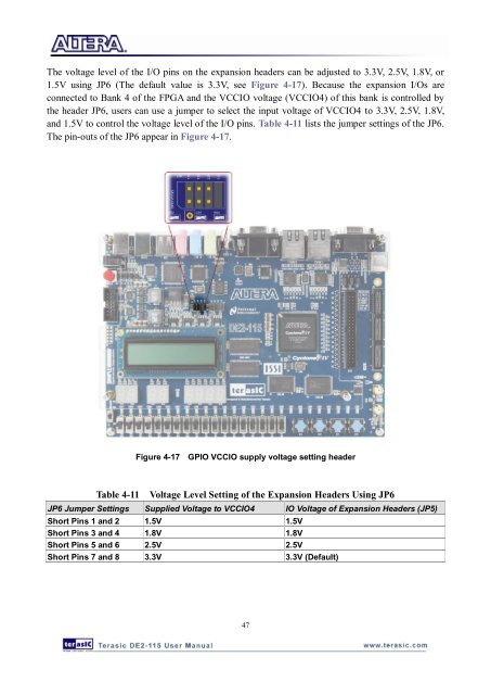
The voltage level of the I/O pins on the expansion headers can be adjusted to 3.3V, 2.5V, 1.8V, or<br />
1.5V using JP6 (The default value is 3.3V, see Figure 4-17). Because the expansion I/Os are<br />
connected to Bank 4 of the FPGA and the VCCIO voltage (VCCIO4) of this bank is controlled by<br />
the header JP6, users can use a jumper to select the input voltage of VCCIO4 to 3.3V, 2.5V, 1.8V,<br />
and 1.5V to control the voltage level of the I/O pins. Table 4-11 lists the jumper settings of the JP6.<br />
The pin-outs of the JP6 appear in Figure 4-17.<br />
Figure 4-17 GPIO VCCIO supply voltage setting header<br />
Table 4-11<br />
Voltage Level Setting of the Expansion Headers Using JP6<br />
JP6 Jumper Settings Supplied Voltage to VCCIO4 IO Voltage of Expansion Headers (JP5)<br />
Short Pins 1 and 2 1.5V 1.5V<br />
Short Pins 3 and 4 1.8V 1.8V<br />
Short Pins 5 and 6 2.5V 2.5V<br />
Short Pins 7 and 8 3.3V 3.3V (Default)<br />
47