
Create successful ePaper yourself
Turn your PDF publications into a flip-book with our unique Google optimized e-Paper software.
GUZUNTY PI<br />
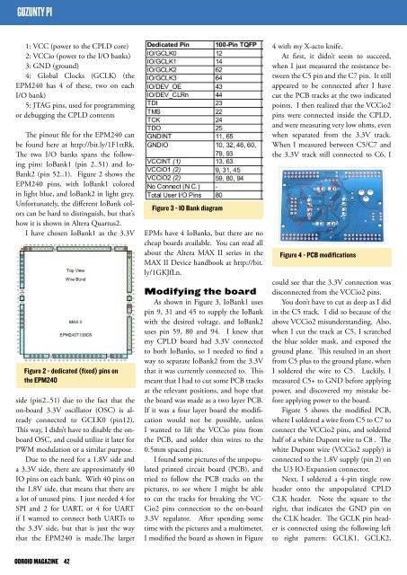
1: VCC (power to the CPLD core)<br />
2: VCCio (power to the I/O banks)<br />
3: GND (ground)<br />
4: Global Clocks (GCLK) (the<br />
EPM240 has 4 of these, two on each<br />
I/O bank)<br />
5: JTAG pins, used for programming<br />
or debugging the CPLD contents<br />
The pinout file for the EPM240 can<br />
be found here at http://bit.ly/1F1ttRk.<br />
The two I/O banks spans the following<br />
pins: IoBank1 (pin 2..51) and Io-<br />
Bank2 (pin 52..1). Figure 2 shows the<br />
EPM240 pins, with IoBank1 colored<br />
in light blue, and IoBank2 in light grey.<br />
Unfortunately, the different IoBank colors<br />
can be hard to distinguish, but that’s<br />
how it is shown in Altera Quartus2.<br />
I have chosen IoBank1 as the 3.3V<br />
Figure 2 - dedicated (fixed) pins on<br />
the EPM240<br />
side (pin2..51) due to the fact that the<br />
on-board 3.3V oscillator (OSC) is already<br />
connected to GCLK0 (pin12).<br />
This way, I didn’t have to disable the onboard<br />
OSC, and could utilize it later for<br />
PWM modulation or a similar purpose.<br />
Due to the need for a 1.8V side and<br />
a 3.3V side, there are approximately 40<br />
IO pins on each bank. With 40 pins on<br />
the 1.8V side, that means that there are<br />
a lot of unused pins. I just needed 4 for<br />
SPI and 2 for UART, or 4 for UART<br />
if I wanted to connect both UARTs to<br />
the 3.3V side, but that is just the way<br />
that the EPM240 is made.The larger<br />
Figure 3 - IO Bank diagram<br />
EPMs have 4 IoBanks, but there are no<br />
cheap boards available. You can read all<br />
about the Altera MAX II series in the<br />
MAX II Device handbook at http://bit.<br />
ly/1GKJfLn.<br />
Modifying the board<br />
As shown in Figure 3, IoBank1 uses<br />
pin 9, 31 and 45 to supply the IoBank<br />
with the desired voltage, and IoBank2<br />
uses pin 59, 80 and 94. I knew that<br />
my CPLD board had 3.3V connected<br />
to both IoBanks, so I needed to find a<br />
way to separate IoBank2 from the 3.3V<br />
that it was currently connected to. This<br />
meant that I had to cut some PCB tracks<br />
at the relevant positions, and hope that<br />
the board was made as a two layer PCB.<br />
If it was a four layer board the modification<br />
would not be possible, unless<br />
I wanted to lift the VCCio pins from<br />
the PCB, and solder thin wires to the<br />
0.5mm spaced pins.<br />
I found some pictures of the unpopulated<br />
printed circuit board (PCB), and<br />
tried to follow the PCB tracks on the<br />
pictures, to see where I might be able<br />
to cut the tracks for breaking the VC-<br />
Cio2 pins connection to the on-board<br />
3.3V regulator. After spending some<br />
time with the pictures and a multimeter,<br />
I modified the board as shown in Figure<br />
4 with my X-acto knife.<br />
At first, it didn’t seem to succeed,<br />
when I just measured the resistance between<br />
the C5 pin and the C7 pin. It still<br />
appeared to be connected after I have<br />
cut the PCB tracks at the two indicated<br />
points. I then realized that the VCCio2<br />
pins were connected inside the CPLD,<br />
and were measuring very low ohms, even<br />
when separated from the 3.3V track.<br />
When I measured between C5/C7 and<br />
the 3.3V track still connected to C6, I<br />
Figure 4 - PCB modifications<br />
could see that the 3.3V connection was<br />
disconnected from the VCCio2 pins.<br />
You don’t have to cut as deep as I did<br />
in the C5 track. I did so because of the<br />
above VCCio2 misunderstanding. Also,<br />
when I cut the track at C5, I scratched<br />
the blue solder mask, and exposed the<br />
ground plane. This resulted in an short<br />
from C5 plus to the ground plane, when<br />
I soldered the wire to C5. Luckily, I<br />
measured C5+ to GND before applying<br />
power, and discovered my mistake before<br />
applying power to the board.<br />
Figure 5 shows the modified PCB,<br />
where I soldered a wire from C5 to C7 to<br />
connect the VCCio2 pins, and soldered<br />
half of a white Dupont wire to C8 . The<br />
white Dupont wire (VCCio2 supply) is<br />
connected to the 1.8V supply (pin 2) on<br />
the U3 IO-Expansion connector.<br />
Next, I soldered a 4-pin single row<br />
header onto the unpopulated CPLD<br />
CLK header. Note the square to the<br />
right, that indicates the GND pin on<br />
the CLK header. The GCLK pin header<br />
is connected using the following left<br />
to right pattern: GCLK1, GCLK2,<br />
<strong>ODROID</strong> MAGAZINE 42