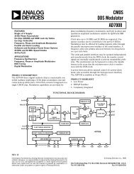
LMX3160 Single Chip Radio Transceiver
LMX3160 Single Chip Radio Transceiver
LMX3160 Single Chip Radio Transceiver
- No tags were found...

Create successful ePaper yourself
Turn your PDF publications into a flip-book with our unique Google optimized e-Paper software.
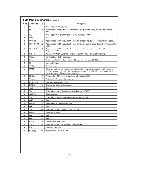
<strong>LMX3160</strong> Pin Diagram (Continued)Pin No Pin Name IO Description17 V P Power supply for charge pump18 D o O Internal charge pump output For connection to a loop filter for driving the input of an externalVCO19 V CC Power supply input for CMOS section of PLL Connect to VBAT20 GND Ground21 Out 0FL o IO Programmable CMOS output Can be used for FastLockTM output (See Programmable Modes)22 Out 1Rx PD IO Programmable CMOS output Can be used for hardwire receiver power down (See ProgrammableModes)23 Out 2Tx PD IO Programmable CMOS output Can be used for hardwire transmitter power down (SeeProgrammable Modes)24 PLL PD I PLL PD e LOW for PLL normal operations PLL PD e HIGH for PLL power saving25 Clock I High impedance CMOS clock input26 Data I Binary serial data input Data entered MSB first High impedance CMOS input27 LE I Load enable input28 OSC IN I Oscillator input29 S Field I DC compensation circuit enable While LOW the DC compensation circuit is enabled and thethreshold is updated through the DC compensation loop While HIGH the switch is opened andthe comparator is held by the external capacitor30 RSSI OUT O Voltage output of the received signal strength indicator (RSSI)31 Thresh O Threshold level to external comparator32 DC COMP IN I Input to DC compensation circuit33 DISC OUT O Demodulated output of discriminator34 GND Ground35 V CC Power supply input to discriminator circuit Connect to VBAT36 QUAD IN I Quadrature input37 V CC Power supply input to limiter output stage Connect to VBAT38 GND Ground39 LIM OUT O Limiter output to the quadrature tank40 GND Ground41 V CC Power supply input for limiter Connect to VBAT42 LIM IN I IF input to the limiter43 GND Ground44 GND Ground45 IF OUT O IF output to bandpass filter46 V CC Power supply input for IF amplifier Connect to VBAT47 IF IN I IF input to IF amplifier48 Rx V REG Supply voltage to external LNA3