Ultra-Low-Power Digital Circuit Design - Microelectronic Systems ...
Ultra-Low-Power Digital Circuit Design - Microelectronic Systems ...
Ultra-Low-Power Digital Circuit Design - Microelectronic Systems ...
- No tags were found...
You also want an ePaper? Increase the reach of your titles
YUMPU automatically turns print PDFs into web optimized ePapers that Google loves.
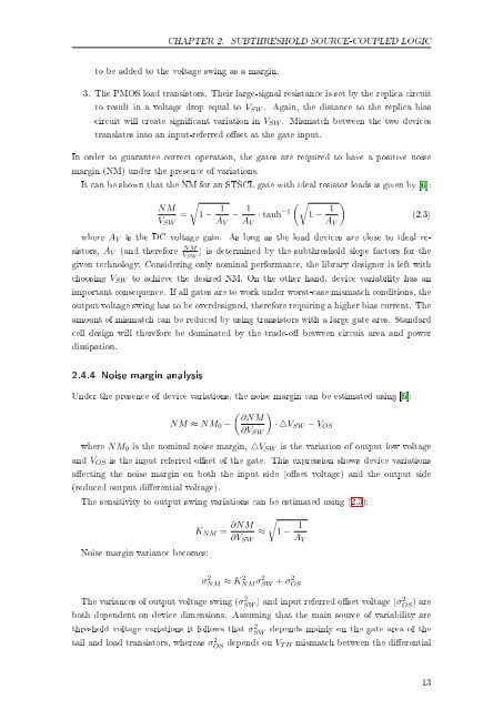
CHAPTER 2.SUBTHRESHOLD SOURCE-COUPLED LOGICto be added to the voltage swing as a margin.3. The PMOS load transistors. Their large-signal resistance is set by the replica circuitto result in a voltage drop equal to V SW . Again, the distance to the replica biascircuit will create signicant variation in V SW . Mismatch between the two devicestranslates into an input-referred oset at the gate input.In order to guarantee correct operation, the gates are required to have a positive noisemargin (NM) under the presence of variations.It can be shown that the NM for an STSCL gate with ideal resistor loads is given by [6]:√NM= 1 − 1 − 1 (√· tanh −1 1 − 1 )V SW A V A V A V(2.3)where A V is the DC voltage gain. As long as the load devices are close to ideal resistors,A V (and therefore NMV SW) is determined by the subthreshold slope factors for thegiven technology. Considering only nominal performance, the library designer is left withchoosing V SW to achieve the desired NM. On the other hand, device variability has animportant consequence. If all gates are to work under worst-case mismatch conditions, theoutput voltage swing has to be overdesigned, therefore requiring a higher bias current. Theamount of mismatch can be reduced by using transistors with a large gate ares. Standardcell design will therefore be dominated by the trade-o between circuit area and powerdissipation.2.4.4 Noise margin analysisUnder the presence of device variations, the noise margin can be estimated using [6]:( ) ∂NMNM ≈ NM 0 − · △V SW − V OS∂V SWwhere NM 0 is the nominal noise margin, △V SW is the variation of output low voltageand V OS is the input referred oset of the gate. This expression shows device variationsaecting the noise margin on both the input side (oset voltage) and the output side(reduced output dierential voltage).The sensitivity to output swing variations can be estimated using (2.3):Noise margin variance becomes:K NM = ∂NM√≈ 1 − 1∂V SW A VσNM 2 ≈ KNMσ 2 SW 2 + σOS2The variances of output voltage swing (σSW 2 ) and input referred oset voltage (σ2 OS ) areboth dependent on device dimensions. Assuming that the main source of variability arethreshold voltage variations it follows that σSW 2 depends mainly on the gate area of thetail and load transistors, whereas σOS 2 depends on V T H mismatch between the dierential13


