

Ultra-Low-Power Digital Circuit Design - Microelectronic Systems ...
Ultra-Low-Power Digital Circuit Design - Microelectronic Systems ...
Ultra-Low-Power Digital Circuit Design - Microelectronic Systems ...
- No tags were found...

You also want an ePaper? Increase the reach of your titles
YUMPU automatically turns print PDFs into web optimized ePapers that Google loves.
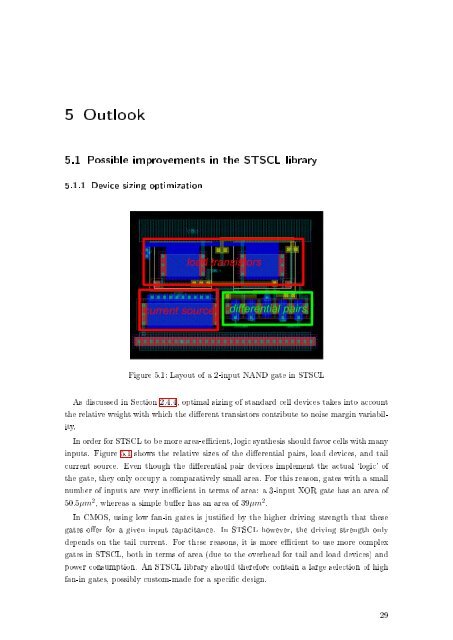
5 Outlook5.1 Possible improvements in the STSCL library5.1.1 Device sizing optimizationFigure 5.1: Layout of a 2-input NAND gate in STSCLAs discussed in Section 2.4.4, optimal sizing of standard cell devices takes into accountthe relative weight with which the dierent transistors contribute to noise margin variability.In order for STSCL to be more area-ecient, logic synthesis should favor cells with manyinputs. Figure 5.1 shows the relative sizes of the dierential pairs, load devices, and tailcurrent source. Even though the dierential pair devices implement the actual `logic' ofthe gate, they only occupy a comparatively small area. For this reason, gates with a smallnumber of inputs are very inecient in terms of area: a 3-input XOR gate has an area of50.5µm 2 , whereas a simple buer has an area of 39µm 2 .In CMOS, using low fan-in gates is justied by the higher driving strength that thesegates oer for a given input capacitance. In STSCL however, the driving strength onlydepends on the tail current. For these reasons, it is more ecient to use more complexgates in STSCL, both in terms of area (due to the overhead for tail and load devices) andpower consumption. An STSCL library should therefore contain a large selection of highfan-in gates, possibly custom-made for a specic design.29


