

Ultra-Low-Power Digital Circuit Design - Microelectronic Systems ...
Ultra-Low-Power Digital Circuit Design - Microelectronic Systems ...
Ultra-Low-Power Digital Circuit Design - Microelectronic Systems ...
- No tags were found...

Create successful ePaper yourself
Turn your PDF publications into a flip-book with our unique Google optimized e-Paper software.
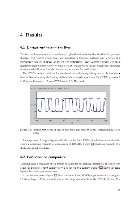
4 Results4.1 <strong>Design</strong> and simulation owThe two implementations were synthesized, placed and routed as described in the previouschapter. The CMOS design was then imported in Cadence Virtuoso and a device andcapacitance extraction from the layout was performed. This extracted netlist was thensimulated using Cadence Spectre, with a VCD (Verilog value change dump) le providingthe input stimuli as well as the correct output values for verication.The STSCL design could not be simulated correctly using this approach. It was simulatedin Nanosim using the Verilog netlist and extracted capacitance le (SPEF) generatedin Cadence Encounter. A supply voltage of 1 V was used.Figure 4.1: Output waveform of one of the regB ip-ops with the corresponding clocksignalA comparison of output signals with the results from VHDL simulation shows that thedesign is operating correctly at a frequency of 100 kHz. Figure 4.1 shows an example of aclock and signal waveform.4.2 Performance comparisonTable 4.1 gives a summary of the results obtained for the implementations of the ECC coreusing the Faraday CMOS library as well as the STSCL library. Figure 4.2 shows the nallayouts for both implementations.It can be seen from Figure 4.2 that the area of the STSCL implementation is roughly8.5 times larger. This is mainly due to the large size of cells in the STSCL library. For23


