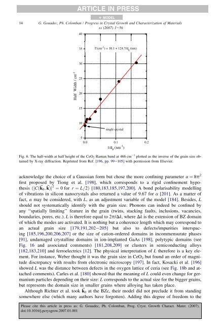
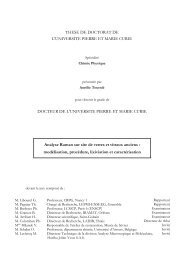
ARTICLE IN PRESS+ MODEL14 G. Goua<strong>de</strong>c, Ph. Colomban / Progress in Crystal Growth and Characterization <strong>of</strong> Materialsxx (2007) 1e564035Γ(cm -1 ) = 10.1 + 124.7/d g (nm)30Half Width / cm -125201510single crystal50.0 0.1 0.21/d g (nm -1 )Fig. 6. The half-width at half height <strong>of</strong> the CeO 2 <strong>Raman</strong> band at 466 cm 1 plotted as the inverse <strong>of</strong> the grain size obtainedby X-ray diffraction. Reprinted from Ref. [196, pp. 99e105] with permission from Elsevier.acknowledge the choice <strong>of</strong> a Gaussian form but chose the more confining param<strong>et</strong>er a ¼ 8p 2first proposed by Tiong <strong>et</strong> al. [198], which corresponds to a rigid confinement hypothesisðjCð~k 0 ;~kÞj 2 ¼ 0 for r ¼ L=2Þ [180,183,185,197,200]. A bond polarisability mo<strong>de</strong>lling<strong>of</strong> vibrations in silicon nanocrystals also r<strong>et</strong>urned a value <strong>of</strong> 9.67 for a [201]. As a matter <strong>of</strong>fact, a may be consi<strong>de</strong>red, with L, as an adjustment variable <strong>of</strong> the mo<strong>de</strong>l [184]. Besi<strong>de</strong>s, Lshould not systematically i<strong>de</strong>ntify with the grain size. Phonons can in<strong>de</strong>ed be confined byany ‘‘spatially limiting’’ feature in the grain (twins, stacking faults, inclusions, vacancies,boundaries, pores, <strong>et</strong>c.). L is therefore equal to 2p/Dk, where Dk is the extension <strong>of</strong> BZ domain<strong>of</strong> which the mo<strong>de</strong>s are activated. It is nothing but a coherence length which may correspond toan actual grain size [179,191,202e205] but also to <strong>de</strong>fects/impurities interspacing[185,196,200,206,207] or the size <strong>of</strong> cation-or<strong>de</strong>red domains in incommensurate phases[91], undamaged crystalline domains in ion-implanted GaAs [198], polytypic domains (seeFig. 16 and associated comments) [181,208,209] or clusters in semiconducting alloys[182,183,210] and ferroelectrics [12]. The physical interpr<strong>et</strong>ation <strong>of</strong> L therefore is a key element.For instance, Weber thought it was the grain size in CeO 2 but found an or<strong>de</strong>r <strong>of</strong> magnitu<strong>de</strong>discrepancy with results from electronic microscopy [197]. In fact, Kosacki <strong>et</strong> al. [196]showed L was the distance b<strong>et</strong>ween <strong>de</strong>fects in the oxygen lattice <strong>of</strong> ceria (see Fig. 18b and attachedcomments). Carles <strong>et</strong> al. [180] showed that the meaning <strong>of</strong> L could even change for germaniumparticles <strong>de</strong>pending on their size: L corresponds to the actual size for the bigger grains,but represents the domain size in smaller grains where alloying has taken place.Although Richter <strong>et</strong> al. took ~k 0 at the BZc, their mo<strong>de</strong>l did not preclu<strong>de</strong> it from standingsomewhere else (which many authors have forgotten). Adding this <strong>de</strong>gree <strong>of</strong> freedom to thePlease cite this article in press as: G. Goua<strong>de</strong>c, Ph. Colomban, Prog. Cryst. Growth Charact. Mater. (2007),doi:10.1016/j.pcrysgrow.2007.01.001
ARTICLE IN PRESS+ MODELG. Goua<strong>de</strong>c, Ph. Colomban / Progress in Crystal Growth and Characterization <strong>of</strong> Materials 15xx (2007) 1e56mo<strong>de</strong>l finds a physical justification in at least two situations. First, when nanoparticles are surroun<strong>de</strong>dby a parent material, the phonons can be reflected at grain boundaries and their interferencescan ‘‘activate’’ mo<strong>de</strong>s away from BZc. This effect was mentioned by Arora <strong>et</strong> al. [211]for CVD-diamond particles embed<strong>de</strong>d in amorphous carbon. They fitted the spectra with asmany as 20 contributions calculated with Eq. (13) at specific values <strong>of</strong> ~k 0 s~0. Second, in their‘‘Random Stacking Fault’’ mo<strong>de</strong>l <strong>of</strong> disor<strong>de</strong>r in silicon carbi<strong>de</strong>, Rohmfeld <strong>et</strong> al. [181,208] useda Bond Polarisability Mo<strong>de</strong>l (BPM) to calculate the influence <strong>of</strong> stacking <strong>de</strong>fects occurring withDL interspacing. They conclu<strong>de</strong>d to the extinction <strong>of</strong> BZc mo<strong>de</strong>s to the benefit <strong>of</strong> mo<strong>de</strong>s withwavevectors equal to k m ¼ (2m þ 1)p/DL; m ¼ 0,1,2. which is analogous to the application <strong>of</strong>Eq. (13) at k m points. Even though disor<strong>de</strong>r and nanom<strong>et</strong>ric dimension effects <strong>of</strong>ten participatesimultaneously to phonon confinement, their relative contributions can theor<strong>et</strong>ically be separatedwhenever ~k 0 is allowed to vary: Disor<strong>de</strong>r will disturb the short range or<strong>de</strong>r and fold the BZ. ~k 0 will be away from BZc and Lshould then be inversely proportional to the <strong>de</strong>nsity <strong>of</strong> <strong>de</strong>fects. If the confinement results from the existence <strong>of</strong> domains in which or<strong>de</strong>r is perfect, typicallynanocrystals, then the activated mo<strong>de</strong>s should be centred in G ð~k 0 ¼ ~0Þ and L will representthe grain size.In Ref. [179], Richter <strong>et</strong> al. attributed the <strong>Raman</strong> signal not accounted for by the PCM t<strong>of</strong>ully amorphous matter (they actually worked on microcrystalline silicon). This explanationwas later used by several authors [191,200,212e214] but should not hi<strong>de</strong> the fact that thePCM is based on approximations and neglects some peculiarities <strong>of</strong> vibrations in<strong>nanomaterials</strong>.(i) The PCM supposes isotropy: as is, the PCM only applies to materials with homogeneousstructure in all directions <strong>of</strong> space (spherical mo<strong>de</strong>l). An ‘‘isotropic dispersion hypothesis’’is probably acceptable for almost any material in the limit <strong>of</strong> ~k 0 close to BZc [184]but integrating Eq. (13) along the main directions <strong>of</strong> the BZ r<strong>et</strong>urns more satisfactoryresults [215]. Carles <strong>et</strong> al. [180] proposed a simple way <strong>of</strong> taking anisotropy into account:all directions are plotted on the same reduced wavevector axis and the wavenumbersare simply averaged. As for G 0 , it is adjusted by means <strong>of</strong> an anisotropy param<strong>et</strong>erbased on the maximum branch ‘‘splitting’’ observed b<strong>et</strong>ween different directions.(ii) The PCM supposes uniform size and shape: another approximation is ma<strong>de</strong> with thePCM when a Gaussian weighing function is introduced in Eq. (9). This assumes all crystalliteshave the same shape e either spherical [181] or orthorhombic [187] e and size,whereas the actual distributions must be taken into account in a mo<strong>de</strong>l <strong>de</strong>scribing reality[184,192,202,216,217].(iii) The PCM neglects surface/interface phonons: the PCM progressively loses its relevancewhen the particle size <strong>de</strong>creases and the surface [218e224]/interface [219,225] mo<strong>de</strong>s(which it does not account for) become prepon<strong>de</strong>rant in the signal. Richter <strong>et</strong> al. [179]were aware <strong>of</strong> this limitation when they proposed the PCM and Roy and Sood [222] simultaneouslyconsi<strong>de</strong>red confined bulk mo<strong>de</strong>s (PCM <strong>de</strong>scription) and surface phonons inCdS/CdSe nanoparticles embed<strong>de</strong>d in glass matrix. The surface mo<strong>de</strong>s in ionic crystalsbecome important below w100 nm [226,227] but can be predicted using a ‘‘DielectricContinuum Approach’’ (DCA). Surface Optical mo<strong>de</strong>s (SO) are expected at wavenumbersn SO in the intermediate region b<strong>et</strong>ween the TO and LO mo<strong>de</strong>s, whose splitting isPlease cite this article in press as: G. Goua<strong>de</strong>c, Ph. Colomban, Prog. Cryst. Growth Charact. Mater. (2007),doi:10.1016/j.pcrysgrow.2007.01.001