Raman Spectroscopy of nanomaterials - institut de chimie et des ...
Raman Spectroscopy of nanomaterials - institut de chimie et des ...
Raman Spectroscopy of nanomaterials - institut de chimie et des ...

Create successful ePaper yourself
Turn your PDF publications into a flip-book with our unique Google optimized e-Paper software.
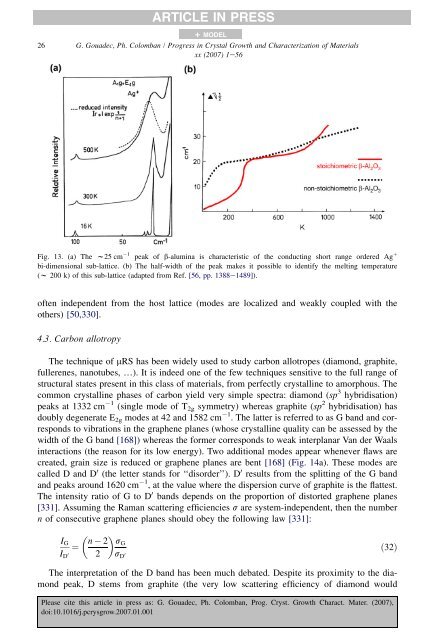
ARTICLE IN PRESS+ MODEL26 G. Goua<strong>de</strong>c, Ph. Colomban / Progress in Crystal Growth and Characterization <strong>of</strong> Materialsxx (2007) 1e56Fig. 13. (a) The w25 cm 1 peak <strong>of</strong> b-alumina is characteristic <strong>of</strong> the conducting short range or<strong>de</strong>red Ag þbi-dimensional sub-lattice. (b) The half-width <strong>of</strong> the peak makes it possible to i<strong>de</strong>ntify the melting temperature(w 200 k) <strong>of</strong> this sub-lattice (adapted from Ref. [56, pp. 1388e1489]).<strong>of</strong>ten in<strong>de</strong>pen<strong>de</strong>nt from the host lattice (mo<strong>de</strong>s are localized and weakly coupled with theothers) [50,330].4.3. Carbon allotropyThe technique <strong>of</strong> mRS has been wi<strong>de</strong>ly used to study carbon allotropes (diamond, graphite,fullerenes, nanotubes, .). It is in<strong>de</strong>ed one <strong>of</strong> the few techniques sensitive to the full range <strong>of</strong>structural states present in this class <strong>of</strong> materials, from perfectly crystalline to amorphous. Thecommon crystalline phases <strong>of</strong> carbon yield very simple spectra: diamond (sp 3 hybridisation)peaks at 1332 cm 1 (single mo<strong>de</strong> <strong>of</strong> T 2g symm<strong>et</strong>ry) whereas graphite (sp 2 hybridisation) hasdoubly <strong>de</strong>generate E 2g mo<strong>de</strong>s at 42 and 1582 cm 1 . The latter is referred to as G band and correspondsto vibrations in the graphene planes (whose crystalline quality can be assessed by thewidth <strong>of</strong> the G band [168]) whereas the former corresponds to weak interplanar Van <strong>de</strong>r Waalsinteractions (the reason for its low energy). Two additional mo<strong>de</strong>s appear whenever flaws arecreated, grain size is reduced or graphene planes are bent [168] (Fig. 14a). These mo<strong>de</strong>s arecalled D and D 0 (the l<strong>et</strong>ter stands for ‘‘disor<strong>de</strong>r’’). D 0 results from the splitting <strong>of</strong> the G bandand peaks around 1620 cm 1 , at the value where the dispersion curve <strong>of</strong> graphite is the flattest.The intensity ratio <strong>of</strong> G to D 0 bands <strong>de</strong>pends on the proportion <strong>of</strong> distorted graphene planes[331]. Assuming the <strong>Raman</strong> scattering efficiencies s are system-in<strong>de</strong>pen<strong>de</strong>nt, then the numbern <strong>of</strong> consecutive graphene planes should obey the following law [331]:I GI D 0 n 2¼2sGs D 0ð32ÞThe interpr<strong>et</strong>ation <strong>of</strong> the D band has been much <strong>de</strong>bated. Despite its proximity to the diamondpeak, D stems from graphite (the very low scattering efficiency <strong>of</strong> diamond wouldPlease cite this article in press as: G. Goua<strong>de</strong>c, Ph. Colomban, Prog. Cryst. Growth Charact. Mater. (2007),doi:10.1016/j.pcrysgrow.2007.01.001