- Page 2: Electronic Circuit Analysis Second
- Page 5 and 6: Copyright © 2008, by Publisher All
- Page 8: PREFACE TO SECOND EDITION Since pub
- Page 11 and 12: x Many Textbooks are referred while
- Page 13 and 14: xii 2.5 Frequency Effects .........
- Page 15 and 16: xiv Unit - 7 Voltage Regulators ...
- Page 17 and 18: xvi C x rx AVI All B.W Ie A=J; IH=
- Page 20 and 21: Brief History of Electronics In sci
- Page 22 and 23: xxi 1975: MSI (Multiplenum, Address
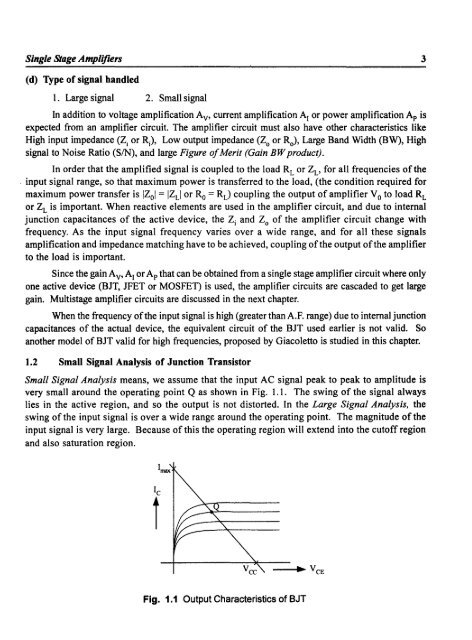
- Page 24 and 25: UNIT - 1 Single Stage Amplifiers In
- Page 28 and 29: Single Stage Amplifiers Ie is in rn
- Page 30 and 31: Single Stage Amplifiers 7 1.3.3 Cur
- Page 32 and 33: Single Stage Amplifiers 9 1.4 Commo
- Page 34 and 35: Single Stage Amplifiers 11 ~ The va
- Page 36 and 37: Single Stage Amplifiers 13 The h-pa
- Page 38 and 39: Single Stage Amplifiers 15 1.5.1 In
- Page 40 and 41: Single Stage Amplifiers 17 Example
- Page 42 and 43: Single Stage Amplifiers 19 ~ is the
- Page 44 and 45: Single Stage Amplifiers 21 1.6 JFET
- Page 46 and 47: Single Stage Amplifiers 23 The pric
- Page 48 and 49: Single Stage Amplifiers 25 But rd»
- Page 50 and 51: Single Stage Amplifiers 27 1. 7 Com
- Page 52 and 53: Single Stage Amplifiers 29 1.9 Gain
- Page 54 and 55: Single Stage Amplifiers 31 1. Write
- Page 56 and 57: UNIT - 2 Multistage Amplifiers In t
- Page 58 and 59: Multistage Amplifiers 35 2.1.5 Band
- Page 60 and 61: Multistage Amplifiers 37 I stage: F
- Page 62 and 63: Multistage Amplifrers 39 The equiva
- Page 64 and 65: Multistage Amplifiers 41 Solution:
- Page 66 and 67: Multistage Amplifiers 43 Example :
- Page 68 and 69: Multistage Amplifiers 45 But Output
- Page 70 and 71: Multistage Amplifiers 47 or ! If;;
- Page 72 and 73: Multistage Amplifiers 49 2.2.5 Midb
- Page 74 and 75: Multistage Amplifiers 51 2.2.8 Phas
- Page 76 and 77:
Multistage Amplifiers 53 R in = Rl
- Page 78 and 79:
Multistage Amplifiers 55 If for a g
- Page 80 and 81:
Multistage Amplifiers 57 2.5 Freque
- Page 82 and 83:
Multistage Amplifiers 59 2.6 Amplif
- Page 84 and 85:
Multistage Amplifiers 61 Ordinary G
- Page 86 and 87:
Multistage A'mpiifzers 63 !c = 1 e
- Page 88 and 89:
Multistage Amplifiers 65 When,f cha
- Page 90 and 91:
Multistage Amplifiers 67 Substituti
- Page 92 and 93:
Multistage Amplifiers 69 2.7.4 Outp
- Page 94 and 95:
Multistage Amplifiers 71 I' can be
- Page 96 and 97:
Multistage Amplifiers 73 The circui
- Page 98 and 99:
Multistage Amplifiers 75 Therefore,
- Page 100 and 101:
Multistage Amplifiers 77 2.9 CE - C
- Page 102 and 103:
Multistage Amplifiers 79 where Ad i
- Page 104 and 105:
Multistage Amplifiers 81 + vee BI B
- Page 106 and 107:
Multistage Amplifiers 83 8 pins. In
- Page 108 and 109:
Multistage Amplifiers 85 23. Compar
- Page 110 and 111:
Multistage Amplifiers 87 1. (a) R-C
- Page 112 and 113:
UNIT - 3 High Frequency Transistor
- Page 114 and 115:
High Frequency Transistor Circuits
- Page 116 and 117:
High Frequency Transistor Circuits
- Page 118 and 119:
High Frequency Transistor Circuits
- Page 120 and 121:
High Frequency Transistor (:ircuits
- Page 122 and 123:
High Frequency Transistor Circuits
- Page 124 and 125:
High Frequency Transistor Circuits
- Page 126 and 127:
High Frequency Transistor Circuits
- Page 128 and 129:
High Frequency Transistor Circuits
- Page 130 and 131:
High Frequency Transistor Circuits
- Page 132 and 133:
High Frequency Transistor Circuits
- Page 134 and 135:
High Frequency ·Transistor Circuit
- Page 136 and 137:
High Frequency Transistor Circuits
- Page 138 and 139:
High Frequency Transistor CIraIIts
- Page 140 and 141:
High Frequency Transistor Circuits
- Page 142 and 143:
High Frequency Transistor Circuits
- Page 144 and 145:
High Frequency Transistor Circuits
- Page 146 and 147:
High Frequency Transistor Circuits
- Page 148 and 149:
High Fri/quency Transistor Circuits
- Page 150 and 151:
High Frequency Transistor Circuits
- Page 152 and 153:
High Frequency Transistor Circuits
- Page 154 and 155:
High Frequency Transistor Circuits
- Page 156 and 157:
High Frequency Transistor Circuits
- Page 158 and 159:
High Frequency Transistor Circuits
- Page 160 and 161:
High Frequency Transistor Circuits
- Page 162 and 163:
High Frequency Transistor Circuits
- Page 164 and 165:
High Frequency Transistor Circuits
- Page 166 and 167:
High Frequency Transistor Circuits
- Page 168 and 169:
UNIT - 4 Power Amplifiers In this U
- Page 170 and 171:
Power Amplifiers 147 4.1.3 Class B
- Page 172 and 173:
Power Amplifiers 149 4.2.2 Transfor
- Page 174 and 175:
Power AmpUfiers 151 The assumption
- Page 176 and 177:
Power Amplifiers 153 VCC-::::,VCE=V
- Page 178 and 179:
Power Amplifiers 155 power. Moreove
- Page 180 and 181:
Power Amplifiers 157 In the low fre
- Page 182 and 183:
Power Amplifiers v f = Effective in
- Page 184 and 185:
Power Amplifiers 161 I max t Ie I m
- Page 186 and 187:
Power Amplifiers 163 i., V s ie is
- Page 188 and 189:
Power Amplifiers 165 P - V 21m OC-
- Page 190 and 191:
Power Amplifiers Po is maximum 2 VC
- Page 192 and 193:
Power Amplifiers 169 a pair of clos
- Page 194 and 195:
Power Amplifiers 171 Both the trans
- Page 196 and 197:
Power Amplifiers 173 Peak collector
- Page 198 and 199:
Power Amplifiers 175 A pushpull con
- Page 200 and 201:
Power Amplifiers 177 12V 0.8: 1 110
- Page 202 and 203:
Power Amplifiers 179 The turns rati
- Page 204 and 205:
Power Amplifzers 181 9ja = Junction
- Page 206 and 207:
Power Amplifzers 183 I. Amplifiers
- Page 208 and 209:
Power Ampiifzers 185 1. What are th
- Page 210:
Power Amplifiers 187 23. TD = ~D; +
- Page 213 and 214:
190 Electronic Circuit Analysis 5.1
- Page 215 and 216:
192 Electronic Circuit Analysis R ,
- Page 217 and 218:
194 Electronic Circuit Analysis Let
- Page 219 and 220:
196 Electronic Circuit Analysis Mag
- Page 221 and 222:
198 Electronic Circuit Analysis M =
- Page 223 and 224:
200 Electronic Circuit Analysis Exp
- Page 225 and 226:
202 Electronic Circuit Analysis L c
- Page 227 and 228:
204 Electronic Circuit Analysu. Sol
- Page 229 and 230:
206 Zon Rjl=RolIl\ Fig. 5.17 ro 2 Z
- Page 231 and 232:
208 Electronic Circuit Analysis Mag
- Page 233 and 234:
210 Electronic Circuit Analysis I.
- Page 236 and 237:
UNIT - 6 Tuned Amplifiers - II In t
- Page 238 and 239:
Tuned Amplifiers - II 21S Let P J =
- Page 240 and 241:
Tuned Amplifiers - II 217 But the d
- Page 242 and 243:
Tuned Amplifiers - II 219 Neglectin
- Page 244 and 245:
Tuned Amplifiers - II 221 Q eff =\-
- Page 246 and 247:
Tuned Amplifiers - II 223 C ,..-__-
- Page 248 and 249:
Tuned Amplifiers - II 225 For a shu
- Page 250 and 251:
Tuned Amplifiers - II 227 1 0) (LA
- Page 252 and 253:
Tuned Amplifiers - II 229 r-------p
- Page 254 and 255:
Tuned Amplifiers - II 231 Solving f
- Page 256 and 257:
Tuned Amplifiers - II 233 So the va
- Page 258 and 259:
Tuned Amplifiers - II 235 1. Draw t
- Page 260 and 261:
UNIT - 7 Voltage Regulators In this
- Page 262 and 263:
Voltage Regulators 239 7.1.1 Differ
- Page 264 and 265:
Voltage Regulators 241 I. The nomin
- Page 266 and 267:
Voltage Regulators 243 7.1.4 Series
- Page 268 and 269:
Voltage Regulators 245 + '13Y .....
- Page 270 and 271:
Voltage Regulators 247 V 2 15.6 R ~
- Page 272 and 273:
Voltage Regulators ==== The error a
- Page 274 and 275:
Voltage Regulators 251 1. The stabi
- Page 276:
Voltage Regulators 253 4. Sampling
- Page 279 and 280:
256 Electronic Circuit Analysis 8.1
- Page 281 and 282:
258 Electronic Circuit Analysis No
- Page 283 and 284:
260 Electronic Circuit Analysis The
- Page 285 and 286:
262 Electronic Circuit Analysis The
- Page 287 and 288:
264 Electronic Circuit Analysis I m
- Page 289 and 290:
266 Electronic Circuit Analysis 8.5
- Page 291 and 292:
268 Electronic Circuit Analysis 8.6
- Page 293 and 294:
270 Electronic Circuit Analysis Xc
- Page 295 and 296:
272 Electronic Circuit Analysis Exa
- Page 297 and 298:
274 Electronic Circuit Analysis ,.2
- Page 299 and 300:
276 Electronic Circuit Analysis Not
- Page 301 and 302:
278 Electronic Circuit Analysjs The
- Page 303 and 304:
280 Electronic Circuit Analysis Exa
- Page 305 and 306:
282 Electronic Circuit Analysis Rec
- Page 307 and 308:
284 - Electronic Circuit Analysis S
- Page 309:
186 Electronic Circuit Analysis 8.7
- Page 312 and 313:
288 Electronic Circuit Analysis 50
- Page 314 and 315:
290 Electronic Circuit Analysis 8.7
- Page 316 and 317:
292 Eleetronic Circuit Analysis 2.
- Page 318 and 319:
294 Electronic Circuit Analysis The
- Page 320 and 321:
296 Electronic Circuit Analysis 1.
- Page 323 and 324:
APPENDIX-l Colour Codes for Electro
- Page 325 and 326:
APPENDIX 301 --=>- ~ / x W --9JE)-
- Page 327 and 328:
APPENDIX 303 Typical Standard Resis
- Page 329 and 330:
APPENDIX-3 Capacitors Capacitance T
- Page 331 and 332:
APPENDIX 30', Paper capacitors are
- Page 333 and 334:
APPENDIX 309 Foil Electrolyte soake
- Page 335 and 336:
APPENDIX-4 Inductors Magnetic Flux
- Page 337 and 338:
APPENDIX 313 J\ II II 1/ II II II (
- Page 339 and 340:
APPENOIX-5 Miscellaneous Ionic Bond
- Page 341 and 342:
APPENDIX 317 Porcelain coating wire
- Page 343 and 344:
APPENDIX 319 More Resistors 14 pin
- Page 345 and 346:
APPENDIX 321 The right-hand rule fo
- Page 347 and 348:
APPENDIX 323 -- Flux N (a) Single-t
- Page 349 and 350:
APPENDIX-6 Circuit Symbols 1 1 - 1
- Page 351 and 352:
APPENDIX-7 Unit Conversion Factors
- Page 353 and 354:
APPENDIX 329 Velocity Units mileslh
- Page 355 and 356:
APPENDIX 331 19 0.912 26.3 35.9 8.0
- Page 357 and 358:
Index Amplifiers 2, 21, 31 A common