Eric Vittoz - IEEE
Eric Vittoz - IEEE
Eric Vittoz - IEEE

You also want an ePaper? Increase the reach of your titles
YUMPU automatically turns print PDFs into web optimized ePapers that Google loves.
TECHNICAL LITERATURE<br />
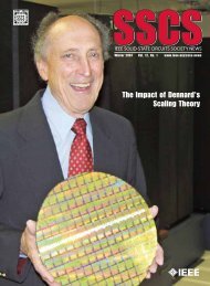
Fig. 5: Analog frequency division techniques; (a) Relaxation<br />
oscillator synchronized by pulses; (b) Step by step<br />
accumulation.<br />
(where CEH was asked to be present, although we<br />
were normally supposed to keep our results secret!).<br />
It is during this period that I made my first visit to<br />
the USA, to attend the ISSCC’64 that was still held in<br />
Philadelphia. During an evening panel on “Minimum<br />
power solid-state devices and circuits”, I was asked by<br />
a friend of Wellinger to say a few words about our<br />
work for an electronic watch. As I can remember, this<br />
idea was considered foolish, if not impossible! This<br />
trip was also a fantastic opportunity to visit a number<br />
of companies and universities and to meet personalities<br />
whose famous names were associated with the<br />
incipient semiconductor technology.<br />
Analog solutions were indeed limiting the number<br />
of components, but the maximum possible dividing<br />
ratio was limited by the precision of these components.<br />
No more than a factor ten per stage could be<br />
expected, even less with the intended integrated versions.<br />
So I looked for an analog solution that could<br />
provide a very large divider ratio even with low-precision<br />
components. This was based on a phaselock<br />
loop as illustrated by Fig. 6.<br />
The loop was made of a low frequency VCO (astable<br />
multivibrator) followed by a pulse shaper, the output p<br />
of which sampled the high frequency input. The result<br />
Fig. 6: Principle of phaselock loop frequency division.<br />
was held by a second order filter that produced the voltage<br />
v c controlling the VCO frequency. The phase of the<br />
VCO could be locked to that of the input signal for any<br />
frequency ratio N = f in / f out that was keeping f out inside<br />
the hold range of the loop. The divider ratio was controlled<br />
by the initial condition imposed to the loop (and<br />
stored in its filter). The hold range could be made large<br />
enough to compensate for even a large error in the natural<br />
frequency of the VCO. The maximum possible ratio<br />
N was limited by the jitter of the VCO. Indeed, this jitter<br />
was producing a phase noise proportional to N, thus a<br />
probability of unlocking increasing with N.<br />
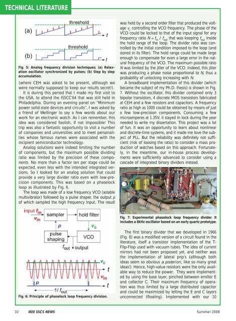
A breadboard implementation of this divider (which<br />
became the subject of my Ph.D. thesis) is shown in Fig.<br />
7. Without the oscillator, this divider contained only 3<br />
bipolar transistors, 4 discrete MOS transistors fabricated<br />
at CEH and a few resistors and capacitors. A frequency<br />
ratio as high as 1000 could be obtained by means of just<br />
a few low-precision components. Consuming a few<br />
microamperes at 1.35V, it stayed in lock during the year<br />
needed to write my dissertation. This project was a lot<br />
of fun. It was an opportunity to learn about nonlinear<br />
and discrete-time systems, and it made me love the subject<br />
of PLL. But the reliability was definitely not sufficient<br />
(risk of loosing the ratio) to consider a mass production<br />
of watches based on this approach. Fortunately,<br />
in the meantime, our in-house process developments<br />
were sufficiently advanced to consider using a<br />
cascade of integrated binary dividers instead.<br />
Fig. 7: Experimental phaselock loop frequency divider. It<br />
includes a 8kHz oscillator based on an early quartz prototype.<br />
The first binary divider that we developed in 1966<br />
(Fig. 8) was a modified version of a circuit found in the<br />
literature, itself a transistor implementation of the T-<br />
Flip-Flop used with vacuum tubes. The idea of current<br />
mirrors had not been proposed yet, and neither was<br />
the implementation of lateral pnp’s (although both<br />
ideas seem so obvious a posteriori, like so many great<br />
ideas!). Hence, high-value resistors were the only available<br />
way to reduce the power. They were implemented<br />
by using the base layer, pinched between emitter E<br />
and collector C. Their maximum frequency of operation<br />
was thus limited by a large distributed capacitor<br />
and could be maximized by letting the E and C layers<br />
unconnected (floating). Implemented with our 10<br />
10 <strong>IEEE</strong> SSCS NEWS Summer 2008