Eric Vittoz - IEEE
Eric Vittoz - IEEE
Eric Vittoz - IEEE

Create successful ePaper yourself
Turn your PDF publications into a flip-book with our unique Google optimized e-Paper software.
TECHNICAL LITERATURE<br />
developing a low-voltage CMOS process. Fritz had<br />
joined CEH after working in the semiconductor<br />
department of General Electric in Syracuse. Following<br />
the key paper of Wanlass and Sah at ISSCC’63 2 , and<br />
strongly supported by Max Forrer, he started developing<br />
low-threshold P-channel devices (a few of<br />
them were used in my experimental PLL frequency<br />
divider) before working on a low-voltage CMOS<br />
process. In 1968, he had assembled a perfectly workable<br />
process 3 . The n-well was obtained by chemically<br />
etching the p-type silicon substrate and epitaxially<br />
refilling it with n-type material. The surface was then<br />
smoothed by mechanical polishing. A molybdenumgold<br />
sandwich was used for the gates (and interconnections)<br />
to obtain a low threshold voltage for both<br />
types of transistors.<br />
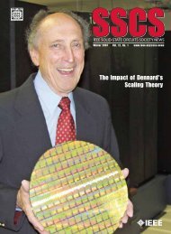
I was asked to design a frequency divider in this<br />
new process. A circuit based on transmission gates<br />
had been presented at ISSCC’67 4 , but its topology was<br />
not suited to group P and N channel devices in two<br />
distinct areas. Instead, I carried out a direct Huffman<br />
synthesis of the divide-by-two function. The resulting<br />
logic equations were implemented by means of two<br />
2-level gates and two inverters (Fig. 12), requiring a<br />
total of 16 transistors (after merging some transistors).<br />
I drew the layout, and Fritz successfully fabricated the<br />
circuit. We measured a current consumption of<br />
10nA/kHz at 1.35V, about 20 times less than the bipolar<br />
dividers used in Beta 21. Since the maximum frequency<br />
at this low voltage was still about 200kHz,<br />
it became possible to increase the frequency of<br />
the oscillator and thereby reduce the size of the<br />
quartz resonator. This frequency was later fixed at<br />
32kHz and is still used nowadays in most electronic<br />
watches.<br />
Fig. 12: First low-voltage CMOS frequency divider.<br />
In 1970, Fritz and his team had developed a new<br />
CMOS process in which the lightly doped p-well was<br />
obtained by solid-to-solid diffusion of boron in a<br />
closed capsule. Standard aluminium gates turned out<br />
to be sufficient to obtain a threshold voltage of about<br />
1 volt for both types of transistors. Our first CMOS LSI<br />
watch circuit was integrated in this new low-voltage<br />
process.<br />
This experimental circuit included the first realization<br />
of digital frequency tuning. The goal was to eliminate<br />
the trimmer capacitor. Instead of adjusting the<br />
frequency of the quartz oscillator, the basic idea was<br />
to adjust the ratio of the frequency divider. The oscillator<br />
could then be optimized for a single frequency,<br />
its stability was not degraded by a trimmer capacitor<br />
and less precision (but no less stability) was required<br />
for the quartz.<br />
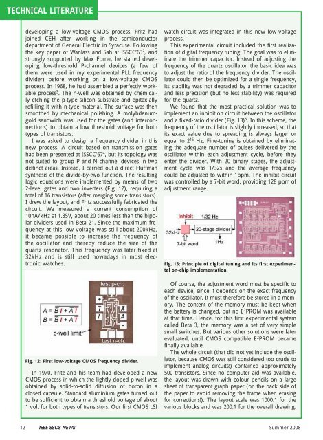
We found that the most practical solution was to<br />
implement an inhibition circuit between the oscillator<br />
and a fixed-ratio divider (Fig. 13) 5 . In this scheme, the<br />
frequency of the oscillator is slightly increased, so that<br />
its exact value due to spreading is always larger or<br />
equal to 2 15 Hz. Fine-tuning is obtained by eliminating<br />
the adequate number of pulses delivered by the<br />
oscillator within each adjustment cycle, before they<br />
enter the divider. With 20 binary stages, the adjustment<br />
cycle was 1/32s and the average frequency<br />
could be adjusted to within 1ppm. The inhibit circuit<br />
was controlled by a 7-bit word, providing 128 ppm of<br />
adjustment range.<br />
Fig. 13: Principle of digital tuning and its first experimental<br />
on-chip implementation.<br />
Of course, the adjustment word must be specific to<br />
each device, since it depends on the exact frequency<br />
of the oscillator. It must therefore be stored in a memory.<br />
The content of the memory must be kept when<br />
the battery is changed, but no E 2 PROM was available<br />
at that time. Hence, for this first experimental system<br />
called Beta 3, the memory was a set of very simple<br />
small switches. But various other solutions were later<br />
evaluated, until CMOS compatible E 2 PROM became<br />
finally available.<br />
The whole circuit (that did not yet include the oscillator,<br />
because CMOS was still considered too crude to<br />
implement analog circuits!) contained approximately<br />
500 transistors. Since no computer aid was available,<br />
the layout was drawn with colour pencils on a large<br />
sheet of transparent graph paper (on the back side of<br />
the paper to avoid removing the frame when erasing<br />
for corrections!). The layout scale was 1000:1 for the<br />
various blocks and was 200:1 for the overall drawing.<br />
12 <strong>IEEE</strong> SSCS NEWS Summer 2008