Eric Vittoz - IEEE
Eric Vittoz - IEEE
Eric Vittoz - IEEE

You also want an ePaper? Increase the reach of your titles
YUMPU automatically turns print PDFs into web optimized ePapers that Google loves.
TECHNICAL LITERATURE<br />
of multi-gate MOS devices and more particularly on<br />
double-gate devices [58], [59].<br />
II. THE EKV DESIGN METHODOLOGY<br />
One of the main features of the EKV model compared<br />
to others is the small number of parameters that it<br />
requires. This obviously simplifies the model and its<br />
implementation, but also the parameter extraction.<br />
Another feature, more important to my eyes, is its<br />
hierarchical structure: indeed the complete compact<br />
model can easily be reduced to the simple hand calculation<br />
model by setting some parameters to specific<br />
values. This allows for a step-by-step approach in<br />
the design of new circuits, starting with the simplest<br />
model coherent with the model used for hand calculation<br />
and progressively adding effects in order to<br />
evaluate their impact on the circuit performance.<br />
Actually, the EKV MOS transistor model was initially<br />
not developed with the aim of having a compact<br />
model for circuit simulation, but rather for having a<br />
simple hand calculation model that can help designing<br />
and sizing circuits that are biased in all modes of<br />
operation including strong and weak inversion but<br />
also the region in between called the moderate inversion.<br />
The available models at that time were simplistic<br />
square-law models that were often inaccurate in<br />
strong inversion and totally wrong in moderate and<br />
weak inversion. The EKV MOS transistor model introduced<br />
the powerful concept of inversion factor (also<br />
called inversion coefficient IC) as the main transistor<br />
design parameter that is more general and replaces<br />
the long-time used overdrive voltage, distinctive of<br />
strong inversion models, but meaningless in weak<br />
inversion. For more than 25 years, E. <strong>Vittoz</strong> and I have<br />
been teaching analog circuit design based on the use<br />
of this concept of inversion factor. This approach<br />
allows for expressing all the important parameters of<br />
a single transistor biased in saturation, such as smallsignal<br />
parameters, including transconductances and<br />
capacitances, noise parameters, versus a single<br />
parameter: the inversion factor. Sweeping the inversion<br />
factor allows exploring all the design space for a<br />
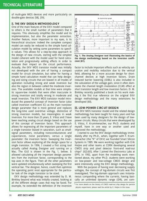
single transistor. In 1996, I created a first sizing tool<br />
actually called Analog Designer and running on a<br />
Mac. The GUI is shown in the Fig. 1, below. It<br />
allowed calculating all the important design parameters<br />
from the inversion factor, corresponding to the<br />
top axes in the figure. Then all the other parameters<br />
were updated simultaneously when sweeping the first<br />
vertical bar. The designer, hence, could then optimize<br />
the operating point most appropriate for the particular<br />
task of the single transistor to be sized.<br />
EKV design methodology was extended by D. M.<br />
Binkley beyond what was initially created, looking at<br />
all the different design cases that may be faced. For<br />
example, he extended the definition of the inversion<br />
Fig. 1. The Analog Designer tool illustrating the basics of<br />
the design methodology based on the inversion coefficient<br />
[61].<br />
factor to include important effects such as velocity saturation<br />
and mobility reduction due to the vertical<br />
field, allowing for a more accurate design for shortchannel<br />
devices at high inversion factors. Drain<br />
induced barrier lowering (DIBL) is also included in<br />
the calculation of the voltage gain, since it often dominates<br />
the channel length modulation (CLM) effect at<br />
short transistor length and low inversion factors. D. M.<br />
Binkley recently published a book on his work making<br />
it the first true reference on the original EKV<br />
design methodology and the many extensions he<br />
developed [60].<br />
III. LOW-POWER CIRCUIT DESIGN<br />
The EKV MOS transistor model and the related design<br />
methodology has been taught for many years and has<br />
been used by many designers for the design of lowpower<br />
circuits. Many circuits that were developped by<br />
E. <strong>Vittoz</strong>, F. Krummenacher, our Ph.D. students and<br />
myself, have in one way or another used and<br />
improved the methodology.<br />
I started to use the EKV design methodology immediately<br />
after my Ph.D., when, together with F. Krummenacher<br />
(the “K” of EKV) we founded Smart Silicon<br />
Systems in 1989. We were working together with Erik<br />
Heijne and other teams at CERN developing several<br />
CMOS strip and pixel detector front-end read-out<br />
chips 3 [62]-[65]. After I joined the Electronics Labs at<br />
EPFL in 1992, apart from the modeling work mentioned<br />
above, my other Ph.D. students were working<br />
on low-power and low-voltage CMOS design and<br />
were intensively using the EKV design methodology.<br />
With the purpose of having ever decreasing supply<br />
voltages, the concept of log-domain circuits was first<br />
investigated. The log-domain approach uses instantaneous<br />
companding where the currents, having basically<br />
an unlimited dynamic range (DR), are com-<br />
3 For more details on the history of CMOS read-out chip design for particle<br />
physics experiment, please read the article by E. Heijne in this issue.<br />
26 <strong>IEEE</strong> SSCS NEWS Summer 2008