Eric Vittoz - IEEE
Eric Vittoz - IEEE
Eric Vittoz - IEEE

Create successful ePaper yourself
Turn your PDF publications into a flip-book with our unique Google optimized e-Paper software.
SSCS<br />
SSCS<br />
<strong>IEEE</strong> SOLID-STATE CIRCUITS SOCIETY NEWS<br />
Summer 2008 Vol. 13, No. 3 www.ieee.org/sscs-news<br />
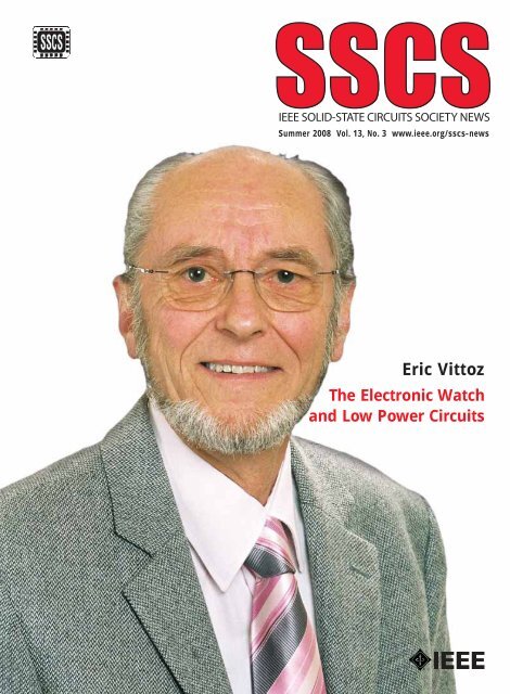
<strong>Eric</strong> <strong>Vittoz</strong><br />
The Electronic Watch<br />
and Low Power Circuits
Editor’s Column<br />
Mary Y. Lanzerotti, IBM, myl@us.ibm.com<br />
Welcome to<br />
the Summer<br />
2008<br />
issue of SSCS News!<br />
As with prior<br />
issues, its goal is to<br />
be a self-contained<br />
resource, with original sources and<br />
new contributions by experts describing<br />
the current state of affairs in technology<br />
in view of the influence of the<br />
original papers and/or patents.<br />
In Summer 2008, we feature the<br />
SSCS News<br />
Editor-in-Chief:<br />
Mary Y. Lanzerotti<br />
IBM T. J. Watson Research<br />
Center<br />
myl@us.ibm.com<br />
Fax: +1 914 945 1358<br />
Technology Editor:<br />
Richard C. Jaeger<br />
Alabama Microelectronics<br />
Center Auburn<br />
University, AL<br />
rj@jaegerengineering.com<br />
Tutorials Editor:<br />
Rakesh Kumar<br />
Technology Connexions<br />
Poway, CA<br />
rakesh@tcxinc.com<br />
Associate Editor for<br />
Europe/Africa:<br />
Tony Harker<br />
Alba Centre Alba Campus<br />
Livingston Scotland EH54 7EG<br />
harker@sli-institute.ac.uk<br />
News Editor:<br />
Katherine Olstein<br />
<strong>IEEE</strong> SSCS<br />
k.olstein@ieee.org<br />
Administrative Committee<br />
President:<br />
Willy Sansen<br />
K. U. Leuven, Belgium<br />
sansen@esat.kuleuven.be<br />
Fax: +32 16 321975<br />
Vice-President:<br />
Bernhard Boser<br />
University of California<br />
Berkeley, CA<br />
Secretary:<br />
David A. Johns<br />
University of Toronto<br />
Toronto, Ontario, Canada<br />
Treasurer:<br />
Rakesh Kumar<br />
Technology Connexions<br />
Poway, CA<br />
Past- President:<br />
Richard C. Jaeger<br />
Alabama Microelectronics<br />
Center<br />
University, AL<br />
Other Representatives:<br />
Representative to Sensors<br />
Council<br />
Darrin Young<br />
Representative from CAS to<br />
SSCS<br />
Domine Leenaerts<br />
Representative to CAS from<br />
SSCS<br />
Un-Ku Moon<br />
work and impact of Dr. <strong>Eric</strong> <strong>Vittoz</strong>,<br />
who has written an extensive lead<br />
article entitled “Electronic Watch and<br />
Low Power Circuits.” I am grateful to<br />
Dr. Erik Heijne for suggesting Dr. <strong>Vittoz</strong><br />
as a potential subject and feature<br />
author, and for his recommendations<br />
of experts who could attest to the<br />
impact of Dr. <strong>Vittoz</strong>’s career on the<br />
development and commercialization<br />
of electronic Swiss watches. Please<br />
be sure to read Dr. Heijne’s Introduction<br />
to this issue on page 4.<br />
<strong>IEEE</strong> Solid-State Circuits Society<br />
Executive Director:<br />
Anne O’Neill<br />
<strong>IEEE</strong> SSCS-West:<br />
1500 SW 11th Avenue #1801<br />
Portland, OR 97201<br />
Tel: +1 732 981 3400<br />
Fax: +1 732 981 3401<br />
Email: sscs@ieee.org<br />
Administrator:<br />
Katherine Olstein<br />
<strong>IEEE</strong> SSCS<br />
445 Hoes Lane<br />
Piscataway, NJ 08854<br />
Tel: +1 732 981 3410<br />
Fax: +1 732 981 3401<br />
Elected AdCom Members at<br />
Large<br />
Terms to 31 Dec. 08:<br />
Wanda K. Gass<br />
Ali Hajimiri<br />
Paul J. Hurst<br />
Akira Matsuzawa<br />
Ian Young<br />
Terms to 31 Dec. 09:<br />
John J. Corcoran<br />
Kevin Kornegay<br />
Hae-Seung (Harry) Lee<br />
Thomas H. Lee<br />
Jan Van der Spiegel<br />
Terms to 31 Dec. 10:<br />
Terri S. Fiez<br />
Tadahiro Kuroda<br />
Bram Nauta<br />
Jan Sevenhans<br />
Mehmet Soyuer<br />
Region 8 Representative:<br />
Jan Sevenhans<br />
Region 10 Representative:<br />
C.K. Wang<br />
Chairs of Standing<br />
Committees:<br />
Awards John J. Corcoran<br />
Chapters Jan Van der Spiegel<br />
Education C.K. Ken Yang<br />
Meetings Bill Bidermann<br />
Membership Bruce Hecht<br />
Nominations Richard C. Jaeger<br />
Publications Glenn Gulak<br />
For detailed contact information,<br />
see the Society e-News:<br />
www.ieee.org/portal/site/sscs<br />
For questions regarding Society business, contact the SSCS Executive Office. Contributions for the<br />
Fall 2008 issue of the Newsletter must be received by 8 August 2008 at the SSCS Executive Office. A<br />
complete media kit for advertisers is available at www.spectrum.ieee.org/mc_print. Scroll down to<br />
find SSCS.<br />
As a result, we are honored to<br />
offer:<br />
(1) “A Short Story of the EKV MOS<br />
Transistor Model,“ by Christian<br />
C. Enz (Swiss Center for Electronics<br />
and Microtechnology);<br />
(2) “Watch Microelectronics: Pioneer<br />
in Portable Consumer<br />
Electronics,” by Mougahed<br />
Darwish, Marc Degrauwe,<br />
Thomas E. Gyger, Gunther<br />
Meusburger, (all at EM Microelectronic-Marin<br />
SA), Jean<br />
Claude Robert (ETA);<br />
(3) “It’s About Time: A Brief Chronology<br />
of Chronometry,” by Thomas<br />
Lee (Stanford University);<br />
(4) “History of the Development of<br />
the Swiss Watch Microprocessors,”<br />
by Christian Piguet (CSEM<br />
Centre Suisse d’Electronique et<br />
de Microtechnique S.A.);<br />
(5) “<strong>Eric</strong> <strong>Vittoz</strong> and the Strong<br />
Impact of Weak Inversion Circuits,”<br />
by Yannis Tsividis<br />
(Columbia University).<br />
Summer ’08 also includes reprints<br />
of one original paper and the first<br />
two pages of two original patents by<br />
Dr. <strong>Vittoz</strong>:<br />
(1) F. Leuenberger and E. <strong>Vittoz</strong>,<br />
“Complementary-MOS Low-<br />
Power Low-Voltage Integrated<br />
Binary Counter,” Proceedings<br />
of the <strong>IEEE</strong>, Vol. 57, No. 9,<br />
September, 1969, pp. 1528-<br />
1532.<br />
(2) E. A. <strong>Vittoz</strong>, “Frequency Divider<br />
Circuit,” U. S. Patent 3,619,646,<br />
Nov. 9, 1971.<br />
(3) W. Hammer, E. A. <strong>Vittoz</strong>, J. Hermann,<br />
H. Choffat, “Timekeeper,”<br />
U. S. Patent 3,895, 485, July 22,<br />
1975.<br />
To accentuate the impact of Dr.<br />
<strong>Vittoz</strong>’s work, I would like to<br />
include two photographs that I<br />
took of the Swatch store in Grand<br />
Central Terminal, New York, NY.<br />
(This store is directly on the walking<br />
path from the train to the subway.)<br />
continued on page 95<br />
2 <strong>IEEE</strong> SSCS NEWS Summer 2008
Summer 2008 Volume 13, Number 3<br />
Photo of<br />
<strong>Eric</strong> <strong>Vittoz</strong><br />
Editor’s Column . . . . . . . . . . . . . . . . . . . . . . . . . . . . . . . . . . . . . . . . . . . . . . . . . . . . . . . . . . 2<br />
President’s Message . . . . . . . . . . . . . . . . . . . . . . . . . . . . . . . . . . . . . . . . . . . . . . . . . . . . . . 4<br />
Introduction . . . . . . . . . . . . . . . . . . . . . . . . . . . . . . . . . . . . . . . . . . . . . . . . . . . . . . . . . . . . 4<br />
Symbiosis in the Technology World, Tony Harker, Associate Editor for Europe/Africa . . . 5<br />
Corrections . . . . . . . . . . . . . . . . . . . . . . . . . . . . . . . . . . . . . . . . . . . . . . . . . . . . . . 73<br />
11<br />
16<br />
53<br />
79<br />
86<br />
TECHNICAL LITERATURE<br />
Electronic Watch and Low-Power Circuits, <strong>Eric</strong> A. <strong>Vittoz</strong> . . . . . . . . . . . . . . . . . . . .7<br />
A Short Story of the EKV MOS Transistor Model, Christian C. Enz . . . . . . . . . . . . 24<br />
Watch Microelectronics: Pioneer in Portable Consumer Electronics,<br />
M. Darwish, M. Degrauwe, T. Gyger, G. Meusburger, J. C. Robert . . . . . . . . . . 31<br />
It’s About Time: A Brief Chronology of Chronometry, Thomas H. Lee . . . . . . . . 42<br />
History of the Development of Swiss Watch Microprocessors, Christian Piguet . . . 50<br />
<strong>Eric</strong> <strong>Vittoz</strong> and the Strong Impact of Weak Inversion Circuits, Yannis Tsividis . . . . . 56<br />
Executive Summary: Advances in Ultra-Low-Voltage Design, J. Kwong,<br />
A. Chandrakasan . . . . . . . . . . . . . . . . . . . . . . . . . . . . . . . . . . . . . . . . . . . . . . . 59<br />
Executive Summary: Gigasensors for an Attoscope, Erik H. M. Heijne, . . . . . . . 60<br />
Complementary-MOS Low-Power Low-Voltage Integrated Binary Counter,<br />
Fritz Leuenberger and <strong>Eric</strong> <strong>Vittoz</strong>, reprinted from Proceedings of the <strong>IEEE</strong>, 57<br />
(9):1528-1532, September, 1969 . . . . . . . . . . . . . . . . . . . . . . . . . . . . . . . . . . . . . 61<br />
Microwatt Switched Capacitor Circuit Design, E. <strong>Vittoz</strong>, presented at a<br />
Summer Course On Switched Capacitor Circuits, June 9-12, 1981, ESAT,<br />
KU Leuven . . . . . . . . . . . . . . . . . . . . . . . . . . . . . . . . . . . . . . . . . . . . . . . . . . . . . . . 66<br />
Frequency Divider Circuit (U.S. Patent No. 3,619,646) <strong>Eric</strong> Andre <strong>Vittoz</strong>, 1971 67<br />
Timekeeper (U.S. Patent No. 3,895,486) W. Hammer, E. <strong>Vittoz</strong>, J. Hermann,<br />
H. Choffat, 1975 . . . . . . . . . . . . . . . . . . . . . . . . . . . . . . . . . . . . . . . . . . . . . . . . . . 69<br />
PEOPLE<br />
Clark Nguyen Presents DL Talk on RF-MEMS in Japan, Katherine Olstein . . . . . . . . . . . 71<br />
New Senior Members . . . . . . . . . . . . . . . . . . . . . . . . . . . . . . . . . . . . . . . . . . . . . . . . . . . . . . 72<br />
Tools: Tips for Making Writing Easier, Part 2: Five-Minute Miracle - Narrow Your<br />
Questions, Shape Your Answers, Peter and Cheryl Reimold . . . . . . . . . . . . . . . . . . . . . . 72<br />
CONFERENCES<br />
ISSCC Student Forum, Anne O’Neill . . . . . . . . . . . . . . . . . . . . . . . . . . . . . . . . . . . . . . . . . .74<br />
2007 VLSI-TSA/DAT Best Paper Awards Presented in April, 2008, Clara Wu<br />
and Elodie Ho . . . . . . . . . . . . . . . . . . . . . . . . . . . . . . . . . . . . . . . . . . . . . . . . . . . . . . . . . . . . .75<br />
Now It’s Japan’s Turn to Host A-SSCC, Koji Kito . . . . . . . . . . . . . . . . . . . . . . . . . . . . . . . . .76<br />
Hot Chips 20: Three Days of the Best in High-performance Chips and<br />
Technologies, Don Draper . . . . . . . . . . . . . . . . . . . . . . . . . . . . . . . . . . . . . . . . . . . . . . . . . .78<br />
Custom Integrated Circuits Conference (CICC) Celebrates 30th Year . . . . . . . . . . . . .79<br />
Sister Conferences ESSCIRC/ESSDERC Meet on 15-19 September, Franz Dielacher . .80<br />
2008 <strong>IEEE</strong> Bipolar/BiCMOS Circuits and Technology Conference to Meet in<br />
Monterey, CA, Marise Bafleur . . . . . . . . . . . . . . . . . . . . . . . . . . . . . . . . . . . . . . . . . . . . . . .81<br />
2008 <strong>IEEE</strong> Compound Semiconductor IC Symposium (CSICS) to Collocate with<br />
BCTM in October, Sorin Voinigescu . . . . . . . . . . . . . . . . . . . . . . . . . . . . . . . . . . . . . . . . . . .82<br />
CHAPTER NEWS<br />
SSCS-Green Mountain Organizes 17th <strong>IEEE</strong> North Atlantic Test Workshop,<br />
P. Nsame . . . . . . . . . . . . . . . . . . . . . . . . . . . . . . . . . . . . . . . . . . . . . . . . . . . . . . . . . . . . . . .84<br />
Oregon State University Student Branch Chapter Inaugurated in March,<br />
Sunwoo Kwon . . . . . . . . . . . . . . . . . . . . . . . . . . . . . . . . . . . . . . . . . . . . . . . . . . . . . . . . . . .85<br />
SSCS NEWS<br />
Sansen and Matsuzawa Visit National Taiwan University, C.K. Wang . . . . . . . . . . . . . .86<br />
Eight Candidates Vie for Five AdCom Positions, Anne O’Neill . . . . . . . . . . . . . . . . . . .87<br />
Call for Nominations for Sensors Awards, Anne O’Neill . . . . . . . . . . . . . . . . . . . . . . . . .94<br />
CEDA Currents . . . . . . . . . . . . . . . . . . . . . . . . . . . . . . . . . . . . . . . . . . . . . . . . . . . . . . . . . .94<br />
Summer 2008 <strong>IEEE</strong> SSCS NEWS 3
President’s Message<br />
Willy Sansen, K. U. Leuven, willy.sansen@esat.kuleuven.be<br />
SSCS members ask me, is hardware<br />
disappearing? (They seem<br />
to be worried.) Is this an observation,<br />
or is it the conclusion of some<br />
hardware vs. software panel?<br />
Where has hardware gone? Has it<br />
gone virtual, or has it been globalized<br />
out?<br />
Hardware is, for example, my car.<br />
It is not gone. I sit in it and I drive<br />
it, thanks to all the software inside.<br />
The chips in my car are also hardware,<br />
but they have been realized<br />
thanks to software.<br />
Our “Red Rag” as a Canvas<br />
The Journal of Solid-State Circuits is<br />
also hardware. It is a thick pack of<br />
paper we are used to receiving every<br />
month by mail. We glance through,<br />
we turn pages, like walking through<br />
a painting exhibit. Once in a while<br />
we stop and allow the content to<br />
seep through. We notice the painter<br />
made it twenty years ago. We try to<br />
understand what it tries to say, but<br />
we don’t. We feel something is there,<br />
but it will take more time to understand.<br />
It will take more effort as well.<br />
Right now we don’t have the time.<br />
We will go through it later, somewhere,<br />
when we have more time.<br />
The JSSC Goes Green<br />
Today the Journal in paper form is<br />
disappearing. Environmentalists have<br />
Introduction<br />
convinced us that sending thousands<br />
of pages to readers who look at only<br />
a few makes too heavy a carbon<br />
print on our precious world. So the<br />
Journal in paper has gone virtual; it<br />
has turned into a passworded list of<br />
numbers on a website. Of course, we<br />
have kept the last paper copy in the<br />
lowest drawer of our desk so we can<br />
show it to our grandchildren; and we<br />
smile at their remarks that this is<br />
what we indulged in some time ago.<br />
So we remember and we still like<br />
the red color of that red rag. Now<br />
the red rag has gone green. It has<br />
been virtualized together, perhaps,<br />
with our desk.<br />
Unpeeling the Circuit Paper<br />
We need our Journal for learning. --<br />
Learning is life, and this we need.<br />
How much have we actually<br />
learned from the JSSC?<br />
Looking at a painting never teaches<br />
you all. Going through a paper<br />
never reveals all its secrets. Nowadays<br />
the circuit “paper” comes in layers.<br />
The title and abstract contain its entire<br />
performance, and it is searchable. As<br />
with a number of technical terms, all<br />
paintings [sorry, technical exhibits] are<br />
revealed and explained and put in a<br />
comparative table with the FOM of its<br />
kind. The next layer goes up or<br />
down. Up are all applications, down<br />
are the circuit details. The paper is<br />
Erik H.M. Heijne, CERN, Erik.heijne@cern.ch<br />
Microelectronics profoundly<br />
impacts consumer products<br />
and habits, and the products<br />
themselves put rigorous constraints<br />
on microelectronics. This reciprocity<br />
is perfectly illustrated by the summer<br />
2008 issue of the SSCS News.<br />
The historical accounts given by<br />
some of the actors show how the use<br />
of microelectronics circuits in wristwatches<br />
has forced them to improve<br />
power usage far beyond earlier limits.<br />
Also required were better understanding<br />
and improved tools for<br />
device and circuit simulation.<br />
About a year ago, I suggested to<br />
Mary Lanzerotti and her colleagues<br />
that <strong>Eric</strong> <strong>Vittoz</strong> and his contributions<br />
to low power microelectronics might<br />
be a good subject for an issue of the<br />
Society News. Mary has implemented<br />
this in a marvelous way by contacting<br />
organized per screen (or slide). Only<br />
one delta of understanding is added<br />
per screen. The longer we follow, the<br />
more our insight is built up. At the<br />
end we see some SPICE files and<br />
curves. Who would actually go that<br />
far? Only someone who wants to use<br />
the circuit. First some money must be<br />
paid, however. On the lowest level, I<br />
can do a redesign, according to my<br />
specs. The design procedure is then<br />
started a few layers higher, and my<br />
version is ready. More money is needed<br />
to get a hardware version, and<br />
some more time.<br />
Has Chip Design Gone Virtual?<br />
This circuit was submitted to the<br />
Journal only three weeks ago. Only a<br />
few comments by a few experts have<br />
been added since then. More will be<br />
added later on, I am sure. I have to<br />
add mine as well, if I use it. Otherwise<br />
much more money is required.<br />
Thus, design has gone virtual<br />
now, or is it the hardware (chip)<br />
which has gone virtual? Has the<br />
design of this hardware gone soft?<br />
A conference is like the premiere of<br />
a painting exhibit. We receive a catalogue<br />
beforehand. Then we get together<br />
with a few colleagues or friends to<br />
make a short tour; we exchange our<br />
impressions, and on the reception at<br />
the end, we have a drink, free for SSCS<br />
members.<br />
and stimulating the authors and by<br />
coordinating the issue that you have<br />
in hand. I am certain that the authors’<br />
enthusiasm and informed accounts<br />
will lead to new ideas and stimulate<br />
many in our community, demonstrating<br />
the dynamic of the <strong>IEEE</strong> as an<br />
international community of engineers<br />
with high profile and great potential,<br />
including expertise in the area of low<br />
power.<br />
4 <strong>IEEE</strong> SSCS NEWS Summer 2008
Symbiosis in the Technology World<br />
Tony Harker, ISLI Alba Centre, tony.harker@sli-institute.ac.uk<br />
Symbiosis has many subtly varied<br />
definitions depending<br />
upon your angle of attack. In<br />
broad terms it can be defined as an<br />
association between two or more<br />
bodies or groups that may benefit<br />
one or all members. When applied<br />
to the high technology world, it can<br />
manifest in multiple ways, such<br />
as straight licence arrangements<br />
between suppliers all the way up<br />
to complex multi-faceted collaborative<br />
agreements between global<br />
bodies. Either way, the outcome<br />
should be of clear benefit to all<br />
involved. Once this arrangement<br />
breaks down, it can easily move<br />
into a no-benefit situation or<br />
indeed, in extreme cases, become a<br />
parasitic relationship.<br />
The trick in any symbiotic<br />
arrangement is to choose your partner<br />
or partners carefully. It is also<br />
vital to bound the relationship with<br />
deliverables which enable you to<br />
track and measure output to help<br />
justify your resource expenditure. In<br />
the commercial world, return on<br />
investment is king. Participants<br />
should always be willing to pause<br />
or indeed cancel arrangements<br />
which do not yield useful results.<br />
One excellent example of where<br />
symbiosis should, and in many<br />
cases does, work effectively is in the<br />
links between the commercial and<br />
academic worlds. This is particularly<br />
evident within Europe, where<br />
there are multiple instances of interand<br />
intra- University/Industry collaborations.<br />
However, one should<br />
not overlook the complexities of<br />
such arrangements and the inherent<br />
frustrations that they may bring to<br />
all parties.<br />
Institutions such as IMEC, based<br />
in Belgium, have a commendable<br />
research record based upon close<br />
links with the nation’s industrial<br />
base. This is mirrored by similar<br />
institutions in other countries, such<br />
as the Fraunhofer Institutes through-<br />
Potential investors, collaborative partners, staff and students mix at iSLI’s 2008<br />
open day.<br />
out Germany, LETI based in France,<br />
and the Institute for System Level<br />
Integration (iSLI) & Scottish Universities<br />
Physics Alliance (SUPA), both<br />
of which are based in the UK.<br />
In addition to the research groupings,<br />
there are also significant collaborations<br />
in which young companies<br />
assist one another by pooling<br />
resources and aim generally to represent<br />
the core of industry through<br />
broad based representation. Speaking<br />
for the UK and Ireland, there are<br />
several excellent examples of such<br />
activity: The National Microelectronics<br />
Institute (NMI) acts as a trade<br />
representative body which, amongst<br />
other things, brokers help to the<br />
overall industry to understand who<br />
and what is available to further their<br />
business. The SetSquared partnership<br />
amongst analogous organisations<br />
in the UK is based in the South<br />
of England and aims to assist young<br />
companies through incubation by<br />
providing direct help from seasoned<br />
entrepreneurs to access funding<br />
sources. MIDAS, based in Ireland, is<br />
a group comprised of individual<br />
companies, local offices of multinationals,<br />
and Universities who pool<br />
their needs to help create a local<br />
critical mass and share training<br />
resources.<br />
More information on these bodies<br />
can be found at:<br />
www.imec.be<br />
www.fraunhofer.de<br />
www.leti.fr<br />
www.sli-instititute.ac.uk<br />
www.supa.ac.uk<br />
www.setsquared.co.uk<br />
www.midas.com<br />
Cross Border Collaboration –<br />
The EU Model<br />
The recently announced European<br />
Institute of Technology (EIT) is a<br />
good example of a response to a<br />
perceived need in a specific geographical<br />
area. First broached during<br />
2005, this pan-European entity<br />
was envisaged as helping to produce<br />
useable, wealth generating<br />
output whilst also fostering academic<br />
growth in the relevant institutions<br />
- a clear example of a true symbiotic<br />
relationship. The EIT has now<br />
gone through the consultative<br />
process and has been granted a<br />
budget in excess of 300M Euro to<br />
cover 2008-2013. The aim of the EIT<br />
is simple: to allow more wealth generation<br />
for the European Union by<br />
integrating education, research, and<br />
business-based innovation into the<br />
Summer 2008 <strong>IEEE</strong> SSCS NEWS 5
“Knowledge Triangle.” The proposed<br />
“hub and spoke” model<br />
includes a central governing body<br />
surrounded by “Innovation Communities”<br />
that are expected to relate<br />
closely to their localised needs. A<br />
key attribute in this case is the inclusion<br />
of the business community,<br />
which will aid the generation of<br />
useable outcome. Whilst still in its<br />
formative stages, the EIT promises<br />
to be an interesting, large scale<br />
attempt at bridging the academic<br />
and commercial world to bring benefits<br />
to all stakeholders.<br />
For more information see<br />
ec.europa.eu/eit<br />
Academic and Commercial Drivers<br />
When dealing with the academic<br />
and commercial worlds, it is vital to<br />
realise that there are fundamental<br />
differences in the way that they are<br />
administered, how they function,<br />
and how goals and targets are set<br />
and met. Typically, academic bodies<br />
are set up to research “blue sky”<br />
topics and any fruits of this research<br />
are captured in the papers and<br />
kudos generated therein. The net<br />
contribution of such bodies is typically<br />
at a high level and adds to the<br />
net intellectual capital of countries<br />
and associated communities.<br />
In many cases, blue sky research<br />
can spin off opportunities for more<br />
practical or applied research with<br />
more potential for commercial<br />
exploitation. It is more usual for symbiosis<br />
to manifest itself at this node<br />
than any other. The reason is very<br />
simple – there is opportunity for<br />
money to be made here in many different<br />
forms including IP licensing,<br />
spinout company formation, and contract-based,<br />
focused research/development.<br />
The commercial world is driven by<br />
very different factors. Companies are<br />
in business to create wealth for their<br />
shareholders. They constantly need<br />
to stay ahead of competition through<br />
innovation, typically enslaved to a<br />
constantly evolving market. In the<br />
commercial world, particularly in the<br />
consumer market, products may have<br />
lifetimes counted in months before<br />
significant revisions are required. This<br />
Demonstrating prototypes to potential investors and researchers can pay dividends<br />
in product development.<br />
in turn heaps more pressure on the<br />
development cycle and inherently<br />
more pressure on the innovation<br />
environment. Staying one step ahead<br />
of the game whilst maintaining margins<br />
keeps a lot of senior executives<br />
awake at night. It is therefore not surprising<br />
that many companies favour<br />
close relationships with academic<br />
partners to help fuel the innovative<br />
process.<br />
Such relationships need to be<br />
handled carefully since they can be<br />
fraught with frustration on both<br />
sides. Some of the more commercially<br />
focused institutions have dedicated<br />
groups that specialize in the<br />
commercial interface. Commonly<br />
known as “Technology Transfer” or<br />
“Research and Enterprise” entities,<br />
such bodies are tasked with translating<br />
the needs and deliverables<br />
between the two worlds. People in<br />
these groups typically hail from<br />
both sides of the fence in that they<br />
can relate to the sometimes orthogonal<br />
requirements.<br />
Engagement Models<br />
When considering how to engage<br />
with any partner, it is fundamental<br />
to set down the terms and expected<br />
outcomes. Whilst this may seem<br />
obvious, it is surprising how many<br />
relationships can break down due<br />
to mismatches in expectation. It is<br />
therefore worthwhile building a<br />
reporting and measurement mechanism<br />
whereby progress can be<br />
measured. This can also aid in<br />
staged payment deals and acts as a<br />
convenient brake if a project starts<br />
to go off the rails. Importantly, the<br />
extent to which this structure is put<br />
in place heavily depends upon the<br />
parties involved and the nature of<br />
the programme. In some cases the<br />
value may lie in the unbounded,<br />
free thinking that academics can<br />
bring into the dynamics. In other<br />
cases closely confined, structured<br />
research may be more applicable to<br />
match the aspirations of the commercial<br />
partner. Either way, whatever<br />
is decided needs to be agreed<br />
upfront and be manageable. It can<br />
be easily argued that reporting and<br />
monitoring is not a value add activity.<br />
Indeed over-monitoring can stifle<br />
creativity and ultimately reduce<br />
the effectiveness of the partnership.<br />
Large and small companies tend<br />
to be driven towards different<br />
engagement models. This is primarily<br />
driven by their spending power<br />
and their ability to mitigate the risk<br />
of slippage or failure to deliver a<br />
money-making result (not all<br />
research ends in a positive answer).<br />
Large companies tend to deal with<br />
more left field research since they<br />
are more easily able to offset this<br />
against other revenue generating<br />
continued on page 58<br />
6 <strong>IEEE</strong> SSCS NEWS Summer 2008
The Electronic Watch and Low-Power Circuits<br />
<strong>Eric</strong> A. <strong>Vittoz</strong>, <strong>IEEE</strong> Life Fellow member, evittoz@ieee.org<br />
A New Research Laboratory<br />
This story starts in 1962 with the foundation of CEH<br />
(Centre Electronique Horloger or “Watchmakers Electronic<br />
Center”). The bipolar junction transistor (BJT)<br />
was 14 years old and had already replaced the vacuum<br />
tube in most electronic systems. A few years had<br />
passed since the invention of the integrated circuit,<br />
followed by that of the planar process by Swiss born<br />
physicist Jean Hoerni.<br />
The Swiss watch industry was flourishing, exporting<br />
about 45 million watches per year for a total value of 1.4<br />
billion Swiss francs. But it was undergoing a deep structural<br />
mutation from its traditional organisation based on<br />
corporatism. The whole watch industry was of a fully<br />
mechanical nature and most of the technical managers<br />
had been educated as traditional watchmakers. However,<br />
for several years, a very few visionary managers had<br />
been watching the recent development taking place on<br />
the other side of the Atlantic Ocean, in this strange new<br />
domain for them called solid-state electronics.<br />
Led by Gerard Bauer, the dynamic director of the<br />
Federation of the Swiss Watch Industry (FH), a research<br />
group representing the major Swiss manufacturers was<br />
created, to evaluate if and how this new electronics<br />
could once be applicable in some way to the wristwatch<br />
itself. Through the long existing LSRH (“Swiss<br />
Laboratory for Watch Research”, founded in the 40’s for<br />
research in all aspects of the mechanical watch), they<br />
entrusted the Swiss Technical Universities with some<br />
limited contracts to evaluate these possibilities. They<br />
received rather negative conclusions, but however<br />
decided that a new joint center would be created to<br />
search for possible new watch systems based on electronics.<br />
After receiving enthusiastic support from Sydney<br />
de Coulon, the general Director of Ebauches SA,<br />
the powerful producer of all Swiss watch components,<br />
they hired Roger Wellinger as technical Director to lead<br />
the project. A Swiss electrical engineer, Roger had<br />
spent 15 years in the USA, first as an Associate Professor<br />
of EE at Illinois State University in Urbana, then<br />
with General Electric in Schenectady.<br />
In 1962 CEH, the new joint research laboratory,<br />
was founded in Neuchâtel by several organisations<br />
representing most of the Swiss watch industry, with<br />
a tentative global budget of 5 million Swiss Francs,<br />
to be released year after year. The general mission<br />
of CEH was to develop new time-keeping devices.<br />
This goal was soon refined into that of developing<br />
an electronic wristwatch, with at least one advantage<br />
with respect to existing watches. No need to<br />
say that, at that time, few people could imagine that<br />
one of the main advantages would be a much lower<br />
TECHNICAL LITERATURE<br />
production cost for a better precision.<br />
There was no real market pull: most people were<br />
happy with the precision of their automatic mechanical<br />
watch. Some electrical watches had recently appeared<br />
on the market, replacing the mechanical drive by an<br />
electromagnetic actuator driven from a small mercury<br />
battery through a mechanical switch. A French patent<br />
was proposing to replace the switch by a transistor<br />
(which was realized a few years later). However, this<br />
modest change did not bring much advantage, and<br />
those approaches were soon abandoned.<br />
The only really new wristwatch was the Accutron<br />
that had been developed for Bulova by Swiss engineer<br />
Max Hetzel. Based on a metallic tuning fork<br />
oscillating at 360Hz and activated by a single transistor,<br />
this revolutionary watch had been commercialized<br />
in 1960. It was, however, still essentially mechanical,<br />
with a complex wheel-ratchet system driving the<br />
set of gears, and at a frequency too low to avoid<br />
being affected by gravity.<br />
The electronic quartz clock had already been invented<br />
by Warren Marrisson in 1928, and transistorized quartz<br />
marine chronometers were just available. Their volume<br />
was 1.5dm 3 , and their power consumption larger than<br />
100mW. Hence a quartz wristwatch did not have to be<br />
invented: it already existed as a system. The “only” challenge<br />
was to reduce its volume to less than 3cm 3 , and to<br />
lower its power consumption by 4 orders of magnitude,<br />
down to less than 10μW. This was the maximum acceptable<br />
power consumption to ensure more than one year<br />
of life for the 1.35V mercury button cell compatible with<br />
the wristwatch volume. This new lab was initially lodged<br />
just under the roof of the LSRH building in Neuchâtel<br />
(Fig. 1). In May 1962, I was the very first electrical engineer<br />
hired at CEH by Roger Wellinger.<br />
Fig. 1: LSRH building in Neuchâtel, Switzerland. During its<br />
first year, CEH was lodged just under the roof of the main<br />
building at the left. It then moved to this wing, where the<br />
process line was installed.<br />
Summer 2008 © 2008 <strong>IEEE</strong> <strong>IEEE</strong> SSCS NEWS 7
TECHNICAL LITERATURE<br />
A Passion for Electricity<br />
I was born in 1938 in Lausanne. As far as I can<br />
remember, I have always been fascinated by electricity.<br />
My grandfather was an electrical engineer working<br />
for a local power company. His cellar was a cave<br />
of treasures, full of various discarded electricity counters.<br />
Back home, I used to take them apart, collecting<br />
the various parts. Most interesting was the sub-millimeter<br />
isolated copper wire of the coils. When I was<br />
about six years old, my first applications for it were<br />
220V in-house electrical networks. To connect the<br />
meccano-made switches and light bulbs, I just had to<br />
scratch the isolation at the wire end with my teeth,<br />
bend it, and put it into the power plug. I learned the<br />
hard way the meaning of closing an electrical loop<br />
when I put my hands both sides of the switch!<br />
Nobody seemed to be really worried by the number<br />
of shocks I received during this early learning period.<br />
However, my father (also an engineer, but in civil<br />
engineering) finally decided that I should go to low<br />
voltage and he mounted an old radio transformer in a<br />
wooden box with just the 6.3V for filament heating<br />
available from outside.<br />
My education was in classical literature, with the<br />
threat of “descending” to scientific if my results were<br />
not good enough (so was the hierarchy of matters at<br />
that time!). But I lost no opportunity to communicate<br />
my passion to my classmates. When their presentations<br />
to the class were about poets and musicians,<br />
mine were about electronic recording and electrical<br />
transformers (with a demo based on a self-made highvoltage<br />
transformer driven by a 4.5V battery chopped<br />
by an electric doorbell!). Applications of Ohm’s law<br />
were the subject of a summer technical contest for<br />
which I built a series of demonstrators.<br />
My interest soon concentrated on electronics,<br />
which at that time was almost synonymous to radio.<br />
At 14, I had built from scratch my first short-wave<br />
receiver, winding the thousands of turns of the<br />
2x350V high voltage and manually sawing and bending<br />
the aluminium plates to mount the components. I<br />
passed my ham radio license at 18 and came “on the<br />
air” with a self-made transmitter, with an output<br />
power of 10W delivered by a Telefunken RL12P35<br />
power tube (Fig. 2 shows a later version of my station).<br />
This was my first contact with the USA and an<br />
excellent opportunity to start practicing my school<br />
English. I still feel the excitement of waiting for an<br />
“opening” of the 10 meters band to contact American<br />
or Australian stations as if they were next door! With<br />
the Internet, the excitement of distant communication<br />
is lost nowadays, but at that time it was achieved with<br />
nothing more than my homemade rig.<br />
I received my technical education from the “Ecole<br />
Polytechnique de l’Université de Lausanne” (EPUL,<br />
that later became EPFL, the Swiss Federal Institute of<br />
Fig. 2: At my homemade ham radio station HB9VZ in 1959.<br />
Technology), where the only professor of electronics<br />
was Roger Dessoulavy. I watched him as a god until<br />
I could finally attend his courses, during the 4th and<br />
last year. Most of the course was based on the vacuum<br />
tube, with just two sessions devoted to the transistor.<br />
Upon my request, my diploma project was part<br />
of a transistorized A/D converter. I then spent one<br />
year as a research assistant, working in the ancient<br />
gardener’s house of EPUL and helping to speed up<br />
this converter to audio frequencies. That’s where<br />
Wellinger found me and asked me to join his new<br />
team. We moved to Neuchâtel with my young wife<br />
Monique. She was going to provide me with an essential<br />
support all along my career.<br />
Initial Research Period<br />
My very first task was to demonstrate that a quartz<br />
clock could be operated with the power consumption<br />
compatible with a wristwatch. I delivered a demonstrator<br />
(Fig. 3) that combined an oscillator circuit with<br />
a 10kHz commercial quartz, followed by 4 divide-byten<br />
stages, in order to reduce the frequency down to<br />
1Hz. These dividers were synchronized astable multivibrators<br />
using 2N1711 planar bipolar transistors produced<br />
by SGS that exhibited a large current gain<br />
much below the microampere level. All of the electronics<br />
was consuming less than 10μA at 1.5V. But the<br />
display was a commercially available electric clock<br />
using a stepping motor and consuming more than<br />
1mW. With this simple demonstrator on the table,<br />
Roger Wellinger had his 1.8 million franc budget for<br />
1963 accepted by the board of directors. The real work<br />
could start, but experienced engineers were needed.<br />
Roger was a very enthusiastic and visionary manager.<br />
Using all possible means, he was able to con-<br />
8 <strong>IEEE</strong> SSCS NEWS Summer 2008
Fig. 3: Microwatt clock demonstrator.<br />
vince a bunch of talented Swiss engineers emigrated<br />
in the USA to abandon their interesting and promising<br />
jobs to come back to Switzerland and bring their<br />
experience to CEH. Among them, Max Forrer left<br />
General Electric in Palo Alto to lead the circuit and<br />
system section (he became my direct boss for the next<br />
27 years!), and Kurt Hübner came to lead the microelectronic<br />
section with his 5-year experience at the<br />
Shockley Semiconductor Lab. The real work then<br />
started on four parallel paths.<br />
Most essential was the building-up of an in-house<br />
IC facility, and the development of a process adapted<br />
to low voltage and very low power. Although the first<br />
functional MOS transistors had already been published,<br />
it was decided to start concentrating on the<br />
more traditional bipolar process. A fully operational<br />
facility, including a mask shop, was installed in the<br />
west wing of the LSRH building (Fig. 1).<br />
The second activity was the search for an adequate<br />
time base. The goal was to obtain a precision better<br />
than 10ppm (corresponding roughly to 1 second per<br />
day) at a frequency lower than 10kHz, to limit the<br />
power needed for frequency division. The size of<br />
existing quartz resonators at this frequency was much<br />
too large, and experts in the field pretended that there<br />
was no way to reduce it without drastically reducing<br />
the quality factor. Hence we first searched for various<br />
types of metallic resonators combined with piezoelectric<br />
or electromagnetic transducers. We even evaluated<br />
a statistical time base using alpha particles emitted<br />
by a radioactive source.<br />
But none of these approaches ended successfully.<br />
It is the merit of Armin Frei, another Swiss engineer<br />
repatriated from the USA, to have attacked and solved<br />
the problem of reducing the size of a sub-10kHz<br />
TECHNICAL LITERATURE<br />
Fig. 4: First prototype of 8192Hz small size quartz resonator<br />
developed at CEH.<br />
quartz resonator. Against all odds and predictions, he<br />
was finally able to mount a miniaturized 8192Hz<br />
quartz oscillating in flexural mode in the vacuum of a<br />
small metallic package (Fig. 4).<br />
The third activity was a search for an adequate display<br />
system. The LCD did not exist yet and the LED<br />
had just been demonstrated. It was decided to rely on<br />
electromechanical solutions, by taking advantage of<br />
the matchmakers’ skills in micromechanics. Various<br />
schemes were evaluated, using electromagnetic and<br />
piezoelectric actuators. Two electromagnetic solutions<br />
were finally retained for the first prototypes.<br />
The fourth activity was in electronics, essentially<br />
evaluating different frequency division techniques. I<br />
was mostly involved in this development; hence, I<br />
can describe it with more details.<br />
The planar technology was very novel, only able to<br />
combine just a few components per chip. The rate at<br />
which this number could be increased was uncertain.<br />
No low-power process was available yet, and we did<br />
not discard the possibility to build the first watch by<br />
using discrete components. Therefore, our first aim<br />
was to minimize the number of components, and we<br />
started by looking into all kinds of analog division<br />
techniques.<br />
One possibility was to use synchronized relaxation<br />
oscillators (Fig 5a). I tried various schemes, including<br />
one based on the tunnel diode (that was considered<br />
a very promising device at that time). Another scheme<br />
consisted in the step-by-step accumulation of some<br />
quantity until a threshold would be reached (Fig. 5b).<br />
I first tried to accumulate magnetic flux in a tiny<br />
toroidal magnet (of the kind used for computer memories<br />
at that time), but the energy per cycle was too<br />
high. A better solution was to accumulate a charge in<br />
a capacitor, in a kind of switched capacitor integrator,<br />
combined with a discharge circuit made of complementary<br />
BJT’s. A hybrid version of a single divide-byeight<br />
stage mounted in a TO5 package was presented<br />
at the 1964 International Congress of Chronometry<br />
Summer 2008 <strong>IEEE</strong> SSCS NEWS 9
TECHNICAL LITERATURE<br />
Fig. 5: Analog frequency division techniques; (a) Relaxation<br />
oscillator synchronized by pulses; (b) Step by step<br />
accumulation.<br />
(where CEH was asked to be present, although we<br />
were normally supposed to keep our results secret!).<br />
It is during this period that I made my first visit to<br />
the USA, to attend the ISSCC’64 that was still held in<br />
Philadelphia. During an evening panel on “Minimum<br />
power solid-state devices and circuits”, I was asked by<br />
a friend of Wellinger to say a few words about our<br />
work for an electronic watch. As I can remember, this<br />
idea was considered foolish, if not impossible! This<br />
trip was also a fantastic opportunity to visit a number<br />
of companies and universities and to meet personalities<br />
whose famous names were associated with the<br />
incipient semiconductor technology.<br />
Analog solutions were indeed limiting the number<br />
of components, but the maximum possible dividing<br />
ratio was limited by the precision of these components.<br />
No more than a factor ten per stage could be<br />
expected, even less with the intended integrated versions.<br />
So I looked for an analog solution that could<br />
provide a very large divider ratio even with low-precision<br />
components. This was based on a phaselock<br />
loop as illustrated by Fig. 6.<br />
The loop was made of a low frequency VCO (astable<br />
multivibrator) followed by a pulse shaper, the output p<br />
of which sampled the high frequency input. The result<br />
Fig. 6: Principle of phaselock loop frequency division.<br />
was held by a second order filter that produced the voltage<br />
v c controlling the VCO frequency. The phase of the<br />
VCO could be locked to that of the input signal for any<br />
frequency ratio N = f in / f out that was keeping f out inside<br />
the hold range of the loop. The divider ratio was controlled<br />
by the initial condition imposed to the loop (and<br />
stored in its filter). The hold range could be made large<br />
enough to compensate for even a large error in the natural<br />
frequency of the VCO. The maximum possible ratio<br />
N was limited by the jitter of the VCO. Indeed, this jitter<br />
was producing a phase noise proportional to N, thus a<br />
probability of unlocking increasing with N.<br />
A breadboard implementation of this divider (which<br />
became the subject of my Ph.D. thesis) is shown in Fig.<br />
7. Without the oscillator, this divider contained only 3<br />
bipolar transistors, 4 discrete MOS transistors fabricated<br />
at CEH and a few resistors and capacitors. A frequency<br />
ratio as high as 1000 could be obtained by means of just<br />
a few low-precision components. Consuming a few<br />
microamperes at 1.35V, it stayed in lock during the year<br />
needed to write my dissertation. This project was a lot<br />
of fun. It was an opportunity to learn about nonlinear<br />
and discrete-time systems, and it made me love the subject<br />
of PLL. But the reliability was definitely not sufficient<br />
(risk of loosing the ratio) to consider a mass production<br />
of watches based on this approach. Fortunately,<br />
in the meantime, our in-house process developments<br />
were sufficiently advanced to consider using a<br />
cascade of integrated binary dividers instead.<br />
Fig. 7: Experimental phaselock loop frequency divider. It<br />
includes a 8kHz oscillator based on an early quartz prototype.<br />
The first binary divider that we developed in 1966<br />
(Fig. 8) was a modified version of a circuit found in the<br />
literature, itself a transistor implementation of the T-<br />
Flip-Flop used with vacuum tubes. The idea of current<br />
mirrors had not been proposed yet, and neither was<br />
the implementation of lateral pnp’s (although both<br />
ideas seem so obvious a posteriori, like so many great<br />
ideas!). Hence, high-value resistors were the only available<br />
way to reduce the power. They were implemented<br />
by using the base layer, pinched between emitter E<br />
and collector C. Their maximum frequency of operation<br />
was thus limited by a large distributed capacitor<br />
and could be maximized by letting the E and C layers<br />
unconnected (floating). Implemented with our 10<br />
10 <strong>IEEE</strong> SSCS NEWS Summer 2008
micron bipolar process, this divider could operate up<br />
to 5kHz for a current drain of 1μA.<br />
Circuit simulators did not exist yet, so circuits had to<br />
be verified on a breadboard before integration. All parasitic<br />
capacitors were extracted manually from the layout,<br />
Fig. 8: First binary frequency divider.<br />
but these were of course smaller than those associated<br />
with the breadboard itself. To circumvent this problem,<br />
the value of all extracted capacitors was multiplied by a<br />
large factor (typically 1000), whereas the frequency was<br />
reduced by the same factor. The dynamic behaviour of<br />
the integrated version could then be predicted with good<br />
precision. We used this simulation technique during<br />
many subsequent years, until circuit simulators and transistor<br />
models at very low current were finally available.<br />
It is this integrated frequency divider that was used<br />
in the first prototypes of the electronic watch.<br />
The First Quartz Wristwatch 1<br />
The efforts of the various groups at CEH came to convergence<br />
with the realization of two different prototypes<br />
of the quartz wristwatch (Fig. 9). Both used the 8192Hz<br />
quartz cantilever developed by Armin Frei, driven by a<br />
symmetrical negative resistance circuit. Prototype Beta 1<br />
needed 13 stages of binary division followed by some<br />
logic to drive the moving coil of a 1Hz stepping motor.<br />
In order to reduce the power consumption, prototype<br />
Beta 2 had only 5 stages of division. The 256Hz output<br />
was driving an electromagnetic resonant motor, with a<br />
ratchet driving the train of wheels. In 1967, ten of these<br />
prototypes were presented at the Neuchâtel Chronometry<br />
Observatory where they pulverized all previous<br />
results. They were then disclosed to our unsuspecting<br />
shareholders in a memorable technical seminar.<br />
The industrial production was organized by CEH in<br />
collaboration with several interested watch companies.<br />
It was decided to start from the Beta 2 prototype<br />
Fig. 9: First prototypes of quartz wristwatch developed by CEH.<br />
TECHNICAL LITERATURE<br />
Fig. 10: First LSI circuit developed for a wristwatch.<br />
to ensure a battery life longer than one year. All the<br />
circuitry was integrated on a single chip, under the<br />
responsibility of Raymond Guye. This very first large<br />
scale integration circuit for a watch (Fig. 10) combined<br />
110 components (NPN transistors, high-value<br />
diffused resistors and junction capacitors) in an area<br />
of 8.7mm 2 , and was consuming 12μA at 1.3V. Several<br />
other modifications of the watch prototype were<br />
introduced to realize the industrial version (Fig. 11)<br />
that was named Beta 21. An electronic module was<br />
supporting the quartz (not visible in the picture), the<br />
plastic encapsulated chip, and an adjustable trimmer<br />
capacitor for fine frequency adjustment. The latter<br />
became the source of many problems and would have<br />
to be eliminated in the future. The components were<br />
fabricated by several Swiss companies, but the circuit<br />
was produced by CEH in the IC facilities of its microelectronic<br />
division. A total of about 6000 units were<br />
delivered, and sold under different Swiss trade names.<br />
Fig. 11: Beta 21, module of the first commercial watch<br />
developed at CEH.<br />
I personally made very few direct contributions to<br />
the development of this first industrial product.<br />
Indeed, since 1967, and in parallel with the drafting of<br />
my Ph.D. dissertation, I was involved in the very early<br />
development of low-voltage CMOS circuits.<br />
Pioneering Low-Voltage CMOS Circuits<br />
While most CEH collaborators were busy working on<br />
the first watch prototypes, Fritz Leuenberger was<br />
Summer 2008 <strong>IEEE</strong> SSCS NEWS 11
TECHNICAL LITERATURE<br />
developing a low-voltage CMOS process. Fritz had<br />
joined CEH after working in the semiconductor<br />
department of General Electric in Syracuse. Following<br />
the key paper of Wanlass and Sah at ISSCC’63 2 , and<br />
strongly supported by Max Forrer, he started developing<br />
low-threshold P-channel devices (a few of<br />
them were used in my experimental PLL frequency<br />
divider) before working on a low-voltage CMOS<br />
process. In 1968, he had assembled a perfectly workable<br />
process 3 . The n-well was obtained by chemically<br />
etching the p-type silicon substrate and epitaxially<br />
refilling it with n-type material. The surface was then<br />
smoothed by mechanical polishing. A molybdenumgold<br />
sandwich was used for the gates (and interconnections)<br />
to obtain a low threshold voltage for both<br />
types of transistors.<br />
I was asked to design a frequency divider in this<br />
new process. A circuit based on transmission gates<br />
had been presented at ISSCC’67 4 , but its topology was<br />
not suited to group P and N channel devices in two<br />
distinct areas. Instead, I carried out a direct Huffman<br />
synthesis of the divide-by-two function. The resulting<br />
logic equations were implemented by means of two<br />
2-level gates and two inverters (Fig. 12), requiring a<br />
total of 16 transistors (after merging some transistors).<br />
I drew the layout, and Fritz successfully fabricated the<br />
circuit. We measured a current consumption of<br />
10nA/kHz at 1.35V, about 20 times less than the bipolar<br />
dividers used in Beta 21. Since the maximum frequency<br />
at this low voltage was still about 200kHz,<br />
it became possible to increase the frequency of<br />
the oscillator and thereby reduce the size of the<br />
quartz resonator. This frequency was later fixed at<br />
32kHz and is still used nowadays in most electronic<br />
watches.<br />
Fig. 12: First low-voltage CMOS frequency divider.<br />
In 1970, Fritz and his team had developed a new<br />
CMOS process in which the lightly doped p-well was<br />
obtained by solid-to-solid diffusion of boron in a<br />
closed capsule. Standard aluminium gates turned out<br />
to be sufficient to obtain a threshold voltage of about<br />
1 volt for both types of transistors. Our first CMOS LSI<br />
watch circuit was integrated in this new low-voltage<br />
process.<br />
This experimental circuit included the first realization<br />
of digital frequency tuning. The goal was to eliminate<br />
the trimmer capacitor. Instead of adjusting the<br />
frequency of the quartz oscillator, the basic idea was<br />
to adjust the ratio of the frequency divider. The oscillator<br />
could then be optimized for a single frequency,<br />
its stability was not degraded by a trimmer capacitor<br />
and less precision (but no less stability) was required<br />
for the quartz.<br />
We found that the most practical solution was to<br />
implement an inhibition circuit between the oscillator<br />
and a fixed-ratio divider (Fig. 13) 5 . In this scheme, the<br />
frequency of the oscillator is slightly increased, so that<br />
its exact value due to spreading is always larger or<br />
equal to 2 15 Hz. Fine-tuning is obtained by eliminating<br />
the adequate number of pulses delivered by the<br />
oscillator within each adjustment cycle, before they<br />
enter the divider. With 20 binary stages, the adjustment<br />
cycle was 1/32s and the average frequency<br />
could be adjusted to within 1ppm. The inhibit circuit<br />
was controlled by a 7-bit word, providing 128 ppm of<br />
adjustment range.<br />
Fig. 13: Principle of digital tuning and its first experimental<br />
on-chip implementation.<br />
Of course, the adjustment word must be specific to<br />
each device, since it depends on the exact frequency<br />
of the oscillator. It must therefore be stored in a memory.<br />
The content of the memory must be kept when<br />
the battery is changed, but no E 2 PROM was available<br />
at that time. Hence, for this first experimental system<br />
called Beta 3, the memory was a set of very simple<br />
small switches. But various other solutions were later<br />
evaluated, until CMOS compatible E 2 PROM became<br />
finally available.<br />
The whole circuit (that did not yet include the oscillator,<br />
because CMOS was still considered too crude to<br />
implement analog circuits!) contained approximately<br />
500 transistors. Since no computer aid was available,<br />
the layout was drawn with colour pencils on a large<br />
sheet of transparent graph paper (on the back side of<br />
the paper to avoid removing the frame when erasing<br />
for corrections!). The layout scale was 1000:1 for the<br />
various blocks and was 200:1 for the overall drawing.<br />
12 <strong>IEEE</strong> SSCS NEWS Summer 2008
Layout rules had to be carefully respected at each step<br />
of the drawing, since remaining errors required the<br />
complete erasing of large layout areas.<br />
No computer assisted the mask making either. The<br />
first step was to report each mask on a special sandwich<br />
of red and white plastic called Rubylith. The red<br />
layer was manually cut on a coordinatograph according<br />
to the pattern, and manually peeled. Although all<br />
divider stages were identical (with only one layout),<br />
their cutting and peeling had to be repeated 20 times.<br />
Most critical was the mask for the contact holes. For<br />
some reason, the Rubylith had to be a negative so that<br />
each of the 1000 contact holes (2 per transistor since<br />
this was a metal-gate process) corresponded to a 2 by<br />
2 millimeter square of red layer left on the white<br />
background. They had a natural tendency to peel<br />
away by themselves, so the final control was a real<br />
nightmare! But the masks were successfully finalized,<br />
and the circuit did work at first silicon, with a current<br />
consumption of 0.45μA at 1.5V.<br />
It should be noticed that the chain of divider stages<br />
is asynchronous, with the advantage of consuming just<br />
a little less than twice the first stage alone. But the timing<br />
of the inhibit signal fed back from the end of the<br />
divider is totally random with respect to that of the<br />
pulses delivered by the oscillator. Therefore, the inhibition<br />
circuit was designed to operate properly, independently<br />
of the order of transition of these two logic<br />
signals. However, this turned out to be insufficient.<br />
Indeed, detailed measurements made by the customer<br />
of a subsequent implementation showed that the circuit<br />
stopped operating correctly just within a very narrow<br />
range of temperature (less than 1 degree Celsius).<br />
The problem was traced back to the fact that, at this<br />
particular temperature, the transitions were exactly<br />
simultaneous. This unexpected situation had not been<br />
considered in the synthesis of the inhibition circuit,<br />
which was later corrected. This example illustrates the<br />
difficulty of implementing asynchronous circuits, even<br />
simple ones. It also shows the necessity to analyze<br />
them in detail, and not only simulate them.<br />
The first industrial application of digital tuning was<br />
developed for Complication SA (owner of the Piaget<br />
brand), with a special 524kHz resonator developed at<br />
CEH by Jean Hermann. Since no non-volatile memory<br />
was available yet, it was decided to store the<br />
adjustment word in a RAM and to extend it to 14 bit.<br />
We had developed a new system, called Beta 4, in<br />
which the adjustment was made automatically by the<br />
watch. Three pulses separated by exactly one second<br />
were injected into the watch by magnetic coupling.<br />
This reference was used by the watch circuit to generate<br />
the adjustment word. I can still remember the<br />
semi-discrete experimental system covering the whole<br />
surface of my test bench, including two elementary<br />
coils providing the coupling (but I have unfortunately<br />
made no photograph).<br />
TECHNICAL LITERATURE<br />
The final product came to the market in 1975 and<br />
included a control box (available at the retailer’s<br />
place). The watch was placed on this box before<br />
pushing a button, and two seconds later its frequency<br />
was adjusted within 1ppm. A special very small<br />
size battery had been added to keep powering the<br />
RAM while the main battery was changed. As technical<br />
designers of the systems, we were disappointed to<br />
discover that the company never advertised its originality.<br />
“You do not want to look inside the belly of a<br />
beautiful girl” was their answer!<br />
In the early 70’s, we kept working on improving<br />
the most basic blocks of the watch, the frequency<br />
divider. It was not yet clear whether low-voltage<br />
CMOS circuits could be produced in large quantities.<br />
Thus, with my colleague Jean Fellrath, we started<br />
exploring the possibility to use purely digital binary<br />
dividers based on BJT NAND gates. Since the most<br />
simple known configurations required 6 gates, I built<br />
a specialized computer based on TTL circuits, which<br />
was searching all possible configurations of n gates<br />
for a possibly simpler divider-by-two. The machine<br />
found a 4-gate structure that just required the control<br />
of a race between two gates 6 . We were trying to<br />
implement it by means of the recently published Integrated<br />
Injection Logic (I 2 L) when the project was<br />
abandoned in favour of CMOS solutions. And I later<br />
found my “new” circuit in the literature!<br />
Our existing CMOS divider cell was driven by complementary<br />
input variables and was therefore sensitive<br />
to a possible race between them. With my collaborator<br />
Walter Hammer, we decided to search for<br />
race-free structures (meaning that no two gates transit<br />
simultaneously), with the goal of increasing the<br />
robustness of the frequency divider and possibly<br />
reducing its power consumption. It also meant that<br />
such structures would have a single input (or would<br />
be what was later called “single-clock circuits”), and<br />
that correct operation would be ensured independently<br />
of the relative speed of the various gates.<br />
But at first we had to give a precise definition of a<br />
logic gate, the elementary building block of all<br />
sequential circuits. We came to the following definition<br />
7 : a logic circuit is a gate if, and only if, it can be<br />
modelled by a single-output delay-free combinatorial<br />
circuit followed by an inertial delay (that filters out<br />
any pulse shorter that the delay value). A gate has<br />
therefore no internal memory. A two-level gate can be<br />
implemented in CMOS by means of series/parallel<br />
combinations of transistors. But it ceases to be a gate<br />
if one input is delayed by more than the output delay<br />
(such an input delay might be due to a higher threshold<br />
value, or to some delay in the input connection).<br />
An inverter is of course always a gate, but a cascade<br />
of 3 inverters cannot be considered as a single gate.<br />
Using this definition, I carried out a computer synthesis<br />
of all race-free divider blocks possible with a<br />
Summer 2008 <strong>IEEE</strong> SSCS NEWS 13
TECHNICAL LITERATURE<br />
given number of gates. The computer was the IBM<br />
1130 of the University of Neuchâtel that was fed by<br />
punched cards. I was coming in the evening with my<br />
stack of cards, retrieving the result the next morning.<br />
It took me many days until my FORTRAN program<br />
was debugged, but finally I got the results, which is<br />
still valid to-day: only one 4-gate race-free divider-bytwo<br />
is possible whereas 9 solutions exist with 5 gates.<br />
The best of these 10 possibilities is the 5-gate structure<br />
illustrated in Fig. 14.<br />
Fig. 14: Race-free divide-by-two cell.<br />
The five gates and their interconnections are<br />
defined by the five equations (or rather logic implications).<br />
The input variable is I, each internal variable A<br />
to E is produced by a gate (D and E by simple inverters),<br />
and the gates are interconnected according to<br />
the set of equations. The corresponding graph of transitions<br />
shows that no more than one variable tends to<br />
transit from any given state; hence there is no race<br />
between variables. The sequence of stable states<br />
shows that each variable transits at half the input frequency<br />
and may thus be used as output of the divider<br />
stage. This circuit was integrated experimentally in a<br />
5μm silicon gate process that had been developed in<br />
the meantime 8 (Fig. 15). At 1.35V, it was consuming<br />
only 1.2nA/kHz, thus about 10 times less than the<br />
previous realization. A maximum frequency of 2MHz<br />
made it possible to use higher quartz frequencies for<br />
special products, such as the Beta 4 mentioned previously.<br />
The process itself was running on a pilot line,<br />
producing a limited quantity of industrial circuits.<br />
The asynchronous divide-by-two cell is the most<br />
elementary non-trivial sequential circuit, and computer<br />
synthesis of race-free solutions was not applicable<br />
to more complex cells. But our younger colleague<br />
Christian Piguet later developed a methodology applicable<br />
to various types of cells, including D and JK<br />
flip-flops 9 .<br />
Returning to 1972, an important contribution was<br />
brought by my senior colleague Henri Oguey. After<br />
Fig. 15: First integrated race-free frequency divider.<br />
developing display motors, Henri had been very<br />
active in the industrialization of Beta 21. Returning to<br />
circuit design, he joined our project on new CMOS<br />
frequency dividers. He soon pointed out that among<br />
all the transistors of a sequential circuit, only some are<br />
active to change the output state of each gate, by<br />
charging or discharging the output capacitor. The others<br />
are just needed to maintain established states<br />
against leakage currents. They are therefore not necessary<br />
if the frequency is high enough.<br />
Fig. 16: Transformation of the static circuit of Figure 14<br />
into its dynamic version. Each transistor is represented<br />
as a circle, with the name of the variable driving its gate.<br />
Only transistors shown in red are needed in the dynamic<br />
divider.<br />
I formalized the idea 10 and immediately tried it on<br />
my new divider. I pulled the non-necessary transistors<br />
out of their sockets in my breadboard simulator.... and<br />
the divider kept working. As illustrated in Fig. 16, the<br />
14 <strong>IEEE</strong> SSCS NEWS Summer 2008
static circuit of 22 transistors was transformed into a<br />
dynamic version of only 10 transistors (the inverters<br />
were not needed any longer, since the transistors driven<br />
by them had been removed). Since the total capacitance<br />
to be switched was reduced, the power consumption<br />
was reduced by about one half. The photograph<br />
shows that the dynamic circuit (D/2) is about half<br />
the area of the static version (S/2). A dynamic divideby-three<br />
cell (D/3) proposed by Oguey 11 is also shown.<br />
A semi-dynamic version was also developed by<br />
exploiting the fact that the short duration of the input<br />
signal could be propagated down to low frequencies<br />
by using A as output variable driving the next stage. I<br />
later carried out a systematic synthesis of race-free<br />
dynamic divide-by-N blocks up to N=6. We then<br />
extended the idea of race-free dynamic CMOS to<br />
other logic blocks, including D, T and JK flip-flops.<br />
Pioneering Weak Inversion for Analog CMOS<br />
Most of a watch chip area is occupied by digital circuits.<br />
But the most critical part, the quartz oscillator,<br />
is indeed an analog circuit. To respect the power limitations,<br />
transistors had to be biased at unusually low<br />
current levels below 1μA. The result of my first measurement<br />
of a MOS transistor at very low current is<br />
shown in Fig. 17.<br />
Fig. 17: First measurement of a MOS transistor at very low<br />
current (annotated copy of my notebook).<br />
This was in April 1967. The transistor was a P-channel<br />
device fabricated in 1966 by Fritz Leuenberger, with a<br />
threshold of about 1 volt. I was deeply surprised to discover<br />
that, when the gate voltage was reduced below its<br />
threshold V T , the transfer characteristics were nicely<br />
exponential across more than 5 decades of drain current.<br />
There was no explanation in the literature, since the transistor<br />
was always characterized by a square law behaviour.<br />
So we painfully started trying to model this strange<br />
behaviour. With my colleague Jean Fellrath, we were<br />
struck by the similarity with the BJT and very excited by<br />
the possibility to implement analog schemes developed<br />
for BJT’s, but with a device needing no control current.<br />
TECHNICAL LITERATURE<br />
Jean started with a known current reference (Fig.<br />
18a), in which the size ratio K between two N-channel<br />
transistors is compensated by the building up of a<br />
voltage across a resistor. On this basis, I developed an<br />
amplitude-controlled quartz oscillator (Fig. 18b). In<br />
this circuit, the oscillation voltage at the gate of the<br />
active transistor of the oscillator is filtered out (by a<br />
non-critical RC filter) at the gate of the K-time larger<br />
device, whereas both transistors share the same DC<br />
component. As the amplitude of oscillation increases,<br />
the bias current delivered to the oscillator decreases,<br />
until equilibrium is reached. Later, the resistor shown<br />
in green line was added to limit the start-up current,<br />
and the oscillator was separated from the regulator for<br />
more flexibility. I am still very proud of this circuit<br />
that, with these modifications, has become a standard<br />
in watch oscillators.<br />
Fig. 18: Analog circuits exploiting weak inversion: (a) Current<br />
reference borrowed from BJT design. (b) Amplitudecontrolled<br />
quartz oscillator.<br />
While we were developing and testing other circuits<br />
exploiting these exponential characteristics, several<br />
authors were publishing models to describe this<br />
“weak inversion” or “sub-threshold” behaviour of<br />
MOS transistors (that appears as a DC leakage current<br />
in CMOS digital circuits). Most remarkable was the<br />
paper by Swanson and Meindl 12 . Indeed, not only did<br />
the authors bring important improvements in modelling<br />
weak inversion, but they also showed that digital<br />
CMOS circuits could operate in weak inversion at a<br />
supply voltage as low as 200mV. But the corresponding<br />
maximum frequency was so low that the idea<br />
was forgotten for the next 30 years!<br />
We put together these various publications, and<br />
developed our own simple model that was directly<br />
applicable to hand-design (Fig. 19). The width-tolength<br />
ratio was originally not included inside current<br />
I D0 . This current was later decomposed in the EKV<br />
model, showing its exponential dependency on the<br />
equilibrium threshold voltage V T0 . This model<br />
includes several features that were kept in later<br />
developments leading to the modern EKV model: the<br />
source-drain symmetry is preserved by defining the<br />
various voltages with respect to the (local) substrate,<br />
and a slope factor n is introduced to characterize the<br />
reduced effect of the gate voltage. It also emphasizes<br />
the similarity with BJT’s. Indeed, it corresponds to the<br />
Ebers-Moll model of a BJT with no base current. But<br />
Summer 2008 <strong>IEEE</strong> SSCS NEWS 15
TECHNICAL LITERATURE<br />
the MOS transistor is a 4-terminal device, with the<br />
gate voltage controlling what would be the specific<br />
current of the BJT.<br />
Fig. 19: Model of the MOS transistor in weak inversion. U T<br />
= kT/q , n is the slope factor and V TO is a bias-independent<br />
threshold voltage.<br />
The model and our various circuits were presented<br />
at ESSCIRC’76 13 , followed by an extended version in<br />
our seminal paper of 1977 14 . I still remember that,<br />
after giving the ESSCIRC paper, a comment from the<br />
floor did seriously question the reliability of analog<br />
circuits based on the “leakage current” of transistors.<br />
Of course, weak inversion is not a leakage current. It<br />
is a well-controlled mode of operation that is only<br />
slightly dependent on process parameters. Circuits<br />
operating in weak inversion have since been produced<br />
by hundreds of millions for applications in<br />
watches.<br />
As already mentioned, all circuits were simulated<br />
on a breadboard, after scaling up the values of circuit<br />
capacitors to render those of the breadboard<br />
negligible. This approach posed a special problem<br />
for simulating quartz oscillators, because no electrical<br />
circuit could simulate the very high quality factor<br />
Q of the resonator. While debugging and optimizing<br />
the oscillator of Beta 21, I had developed a special<br />
technique to solve this problem. It was based on the<br />
fact that with such a high Q, the exchange of energy<br />
between the circuit and the resonator can only<br />
take place at the fundamental frequency. The nonlinear<br />
circuit, including the non-motional part of the<br />
quartz resonator, was measured by injecting a sinusoidal<br />
current. The resulting voltage was filtered (by<br />
means of a band pass filter precisely tuned to the<br />
measurement frequency) to obtain the amplitude<br />
and phase of its fundamental component. The result<br />
was then divided by the value of the injected current<br />
to obtain the circuit impedance for the fundamental<br />
frequency Z c(1) (Fig. 20).<br />
Fig. 20: Splitting of a quartz oscillator for precise simulation<br />
of amplitude and frequency. Stable oscillation is<br />
obtained for Z c(1) = Z m [15] .<br />
This is a very powerful technique 15 , capable of simulating<br />
not only the amplitude of oscillation, but also<br />
the precise amount by which the circuit is pulling the<br />
frequency of oscillation away from the (series)<br />
mechanical resonant frequency of the quartz. It is still<br />
very useful today, since it can be applied to computer<br />
simulation as well. It provides much more insight and<br />
precision than the standard lengthy time simulation.<br />
An example of full-blown version of watch oscillator<br />
with very low power consumption is illustrated in<br />
Fig. 21 16 . This circuit was fabricated in a bi-doped<br />
polysilicon process: in order to minimize the threshold<br />
voltage of both types of transistor, the polysilicon<br />
gate layer was p-type for P-channel transistors, and n-type<br />
for N-channel devices. Hence, a lateral diode appeared at<br />
each transition inside the polysilicon layer (normally, it<br />
had to be short-circuited). The first application of this<br />
diode was proposed by Henri Oguey: he used its large<br />
leakage current to maintain some logic states in dynamic<br />
circuits, in a scheme called resistance-CMOS circuits 17 . In<br />
this oscillator, they were used either as floating diodes, or<br />
to replace high-value resistors, by using quads of diodes<br />
to obtain symmetrical voltage-current characteristics. As a<br />
result, no real resistor was needed, and the total current<br />
drain was less than 100nA at 32kHz, almost constant for<br />
a supply voltage ranging from 0.8 to 3 volts. The regulator<br />
itself consumed only 5% of this current.<br />
Fig. 21: Full circuit of a quartz oscillator. The regulator has<br />
been separated from the core of the oscillator, with an<br />
amplifier added to drive the frequency divider.<br />
In 1975, I started the first course on integrated circuit<br />
design at EPFL in Lausanne. I specially empha-<br />
16 <strong>IEEE</strong> SSCS NEWS Summer 2008
sized low-power devices and circuits, thereby initiating<br />
a culture that has been pursued and expanded by<br />
several of my students. CEH had introduced a multicircuit<br />
chip program (a precursor of multi-project<br />
wafers) that was running every three months, so my<br />
students could design small circuits and measure<br />
them after integration.<br />
Besides the small pilot line of CEH, low-voltage<br />
CMOS circuits were produced by Faselec AG in<br />
Zurich, and by EM Microelectronic Marin SA, close to<br />
Neuchâtel.<br />
Further Developments in Low-Power CMOS Devices<br />
and Circuits<br />
The work on most basic circuits for the watch was terminated<br />
around 1977, but an important step still had<br />
to be made: the watch microprocessor. I must confess<br />
that, as the head of CEH circuit design activities, I was<br />
not convinced of the real need for such a development.<br />
But a workgroup was created, including partners<br />
from EPFL, from the University of Neuchâtel and<br />
from the watch industry. This group, led by my young<br />
collaborators Christian Piguet and Jean-Felix Perotto,<br />
started working on the idea of long instructions, to<br />
minimize the rate of memory access. This was the<br />
beginning of an original series of low-power microprocessors<br />
especially designed for watches (see the<br />
article by C. Piguet in this issue). The flexibility<br />
offered by the approach soon rendered it essential,<br />
and nowadays all electronic watches include a special<br />
microprocessor.<br />
The watch also needed some auxiliary circuits.<br />
Among them was a circuit detecting the end of the<br />
battery life. Based on a voltage measurement, it<br />
required a precise voltage reference on the CMOS<br />
chip. We developed our first band gap reference by<br />
combining the base-emitter voltage of the vertical BJT<br />
available in CMOS with a PTAT voltage produced by<br />
MOS transistors in weak inversion 18 . Another reference<br />
imagined by Oguey was again exploiting the bidoped<br />
poly process. It was using the voltage difference<br />
of about one band gap between the threshold<br />
voltage of two N-channel transistors with opposite<br />
types of gate doping 19 .<br />
At that time, our low-power CMOS circuit research<br />
had been extended much beyond traditional watch<br />
circuits, this for two main reasons. One was the need<br />
to serve customers outside the watch industry. The<br />
other was our dream to introduce many other functions<br />
in the watch. Our reasoning was that since the<br />
watch occupies a unique position on its owner’s arm,<br />
it could and should provide several useful functions<br />
or services. Many possibilities were proposed: calculator,<br />
electronic money, electronic key, communication<br />
device, electronic compass, altimeter, personal<br />
data storage, and physiological check of the wearer.<br />
Even though some of these additional functions have<br />
TECHNICAL LITERATURE<br />
later been introduced in special watches (including a<br />
GPS receiver that was not yet conceivable in the midseventies),<br />
this dream of a multifunctional watch<br />
never came to reality. The main technical reason is<br />
the difficulty to manually enter information in a small<br />
device such as a watch. Not that we did not try: a<br />
variety of input devices were developed and tested,<br />
essentially based on capacitive sensors implemented<br />
on the watch glass. Another reason is that a watch is<br />
considered a piece of jewellery rather than a technical<br />
device (unlike today’s portable phones).<br />
We were given a lot of freedom to explore a wide<br />
variety of low-power building blocks. In this framework,<br />
our colleague Henri Oguey proved to be particularly<br />
creative: his 26 notebooks are a mine of<br />
novel ideas, most of them unpublished or even not<br />
tested. A good example is the switched current mirror<br />
that he imagined in 1977 (Fig. 22). The explanation<br />
in French in this figure can be translated into<br />
“obtain the same effect as with two perfectly identical<br />
transistors”. For some obscure reason, we did not<br />
apply for a patent, but I was excited by the idea and<br />
I made a test circuit in one of our multi-circuit chips.<br />
This circuit remained unmeasured (lack of time?) till<br />
the mid-80’s, when I gave it to my student George<br />
Wegmann, as a starting point for his Ph. D. thesis.<br />
George made an excellent work, integrating an optimized<br />
version, and proving by extensive measurements<br />
that such a mirror could reach a precision as<br />
good a 0.1% 20 . At the end of 1988, he was ready to<br />
publish his results when Daubert et al. published the<br />
principle that they named a current copier 21 .<br />
Fig. 22: Excerpt of Oguey’s notebook dated May 1977.<br />
Discussions with Henri Oguey were also at the origin<br />
of a new scheme for accurate compensation of<br />
offset in amplifiers 22 . In this scheme, an offset compensation<br />
voltage is stored, not at the main input of<br />
the amplifier, but at an auxiliary input of lower sensitivity.<br />
The effect of charge injection can thereby be<br />
reduced by a large factor.<br />
After the idea of switched capacitor (SC) circuits<br />
was first published in 1977 23 , we applied it to very<br />
low-power circuits. My first realization was a quasisinusoidal<br />
SC oscillator, intended as a VCO for a tracking<br />
filter, and consuming less than 50nA 24 . As I can<br />
Summer 2008 <strong>IEEE</strong> SSCS NEWS 17
TECHNICAL LITERATURE<br />
remember, the framework was the search for a possible<br />
watch-to-watch communication, using a very narrow<br />
bandwidth to minimize power. We later developed<br />
several versions of low-power SC circuits, in<br />
collaboration with EPFL 25, 26 . I demonstrated that<br />
operational amplifiers with low output impedance<br />
should be replaced by OTA’s in order to minimize<br />
noise 27 . By operating the transistors in weak inversion,<br />
their intrinsic voltage gain was maximum, so<br />
that more than 100dB of gain could be obtained in a<br />
single cascoded stage (although a cascode is indeed a<br />
very special 2-stage configuration). Hence no phase<br />
compensation was needed and the architecture of the<br />
OTA was very simple. But slew rate limitations were<br />
aggravated by the low bias current level, and we had<br />
to develop some schemes for class AB operation 28 .<br />
The principle of one of our new schemes is illustrated<br />
in Fig. 23 29 . The tail current of the input differential<br />
pair is increased proportionally to the difference<br />
of its two output currents. For a proportionality factor<br />
D≥1, the differential transconductance increases with<br />
the input voltage, instead of decreasing to zero as in<br />
a normal differential pair (D=0).<br />
Fig. 23: Principle of a class AB amplifier and transfer characteristics<br />
in weak inversion.<br />
At low supply voltage, the problem of charge injection<br />
by switches (also called clock feedthrough) was<br />
particularly serious. In order to be able to reduce it by<br />
a compensation technique, I carried out the first<br />
detailed analysis of this important problem. This<br />
analysis, based on an equivalent circuit, was originally<br />
only presented at a course in Leuven 27 (and also<br />
published in an obscure journal). It was later confirmed<br />
by other authors 30 , and by detailed measurements<br />
in the framework of our work on switched mirrors<br />
at EPFL 31 .<br />
Latch-up was an important problem in the early<br />
time of CMOS. We discovered it accidentally, before it<br />
had been reported in the literature. My colleague Jean<br />
Hermann was developing a new type of quartz resonator,<br />
and he wanted to carry out long-term measurements<br />
inside an oven. For this purpose, I gave him<br />
one of my recently developed oscillator chips, powered<br />
by a big 10Ah battery. After a few days, he called<br />
me: the oscillator had stopped and the battery was<br />
empty. I took the system back to my lab and measured<br />
it with a new battery; it was working perfectly,<br />
so I send it back to him. This cycle was repeated several<br />
times. While I was once more measuring the circuit,<br />
the current suddenly jumped by 4 orders of magnitude<br />
when I switched on my big oscilloscope. It<br />
returned to its microampere level after switching off<br />
and on the supply voltage. Although we had stopped<br />
designing bipolar circuits, I had always kept an interest<br />
in the BJT. So I was quickly able to identify a<br />
thyristor effect. A model made it easy to understand<br />
what should be done to avoid the problem. Latch-up<br />
could easily be eliminated in sub-microampere circuits,<br />
such as watch circuits: A minimum latch-up current<br />
of about 1mA was guaranteed by applying adequate<br />
layout rules, and a 2kΩ poly resistor was placed<br />
in series with the 1.5V battery, limiting the maximum<br />
current below this value.<br />
My sustained interest for the BJT made me suggest<br />
to operate a standard MOS transistor as a lateral BJT<br />
(which looks obvious, at least a posteriori, given the<br />
structural similarity of the two types of devices). After<br />
negative results obtained by some collaborators, I was<br />
not discouraged and decided to measure it myself. I<br />
took care to consider it as a 5-terminal device (the 4<br />
terminals of the MOS transistor in its well, and the<br />
substrate), and it worked as expected. My first application<br />
was a multiple cascoded current mirror shown<br />
in Fig. 24. The same devices could be operated as<br />
MOS transistors or as lateral BJT’s, to demonstrate the<br />
drastic improvement in precision. I also demonstrated<br />
a band gap voltage reference and a low-noise amplifier<br />
59 . Figure 25 shows a later measurement of 1/f<br />
noise, in which the decreasing gate voltage V G is compensated<br />
by a more negative source voltage V S to<br />
maintain the drain current I D constant (at 1μA). Operation<br />
is therefore progressively moved from MOS to<br />
BJT, showing a dramatic reduction of flicker noise.<br />
Fig. 24: Multiple cascode current mirror. Each inner concentric<br />
device can be configured as a MOS transistor or as<br />
a lateral BJT.<br />
Weak inversion provides several advantages that<br />
can be exploited in low-power circuits. But this mode<br />
of operation also has some drawbacks, the most<br />
important being the poor precision of current mirrors.<br />
Hence, even in very low-power circuits, the various<br />
18 <strong>IEEE</strong> SSCS NEWS Summer 2008
Fig. 25: Flicker noise measurements (from Stephan Cserveny,<br />
unpublished).<br />
transistors must usually be biased with various<br />
degrees of inversion, depending on their function.<br />
This is the reason why we needed a model covering<br />
all levels of current, from weak to strong inversion. In<br />
collaboration with Stefan Cserveny, Henri Oguey<br />
developed a model called CEMOS that was an important<br />
step towards our later EKV model. They introduced<br />
the notion of control voltage (that became the<br />
pinch-off voltage in EKV). They also emphasized the<br />
symmetry of the transistor by expressing the drain<br />
current as the difference of two values of the same<br />
function, one calculated at the source, the other at the<br />
drain (these two values became the forward and<br />
reverse components of drain current in the EKV<br />
model). The function itself was changing smoothly<br />
from the exponential of weak inversion to the square<br />
law of strong inversion, by means of a mathematical<br />
interpolation.<br />
In 1983, the CEH research laboratories were<br />
merged into CSEM (a French acronym for Swiss Centre<br />
for Electronics and Microtechnology), a newly<br />
founded organization partially supported by the Swiss<br />
government. During its more than 20 years of existence,<br />
CEH had provided a very open research environment<br />
with a lot of research freedom. The definition<br />
of most of the projects was sufficiently general to<br />
allow the researchers to explore new ideas inside<br />
wide domains. I like to compare this kind of exploration<br />
with the exploration of unknown territories of<br />
the World. We were exploring in particular the continent<br />
of very low-power circuits (we called them<br />
micropower circuits), with no predefined milestones<br />
(what are milestones in the exploration of a terra<br />
incognita?). The cafeteria was always a place of<br />
intense technical discussions and exchanges between<br />
designers and process specialists. We were given the<br />
time and the freedom to generalize our ideas and to<br />
conceptualize them (a very important step to progress<br />
in research). Of course, there were dead ends, but<br />
they often could be transformed into new ideas applicable<br />
elsewhere. The lack of computer resources<br />
forced us to use analytical approaches, which give<br />
much more insight than computed sets of numbers or<br />
plots (the computer is of course an invaluable com-<br />
TECHNICAL LITERATURE<br />
plementary tool, but should not replace the analysis<br />
as is does too often nowadays). Overall, this CEH<br />
period was a fantastic adventure for all of us.<br />
Low-Power Circuits at EPFL and CSEM<br />
CSEM was more development-oriented, with welldefined<br />
specifications to be reached in a well-defined<br />
period of time. I moved more of my personal research<br />
to EPFL in collaboration with my Ph.D. students.<br />
A very imaginative student, François Krummenacher<br />
had independently solved the problem of sensitivity<br />
of SC circuits to parasitic capacitors during his<br />
Diploma work. He later developed a low-power SC<br />
filter approach with intrinsic double correlated sampling<br />
to reduce the 1/f noise 32 , and his Ph.D. thesis<br />
was about the optimisation of very low-power SC filters.<br />
As a first assistant, he later developed along the<br />
years a multiplicity of novel low-power circuits,<br />
including continuous-time filters 33 .<br />
François also helped me supervise the Ph.D. project<br />
of Christian Enz on high-precision CMOS micropower<br />
amplifiers. It is in this framework that previous developments<br />
of a MOS model at CEH were pursued and<br />
extended at EPFL. This new model was later called<br />
EKV, after its first publication by the three of us 34 .At<br />
this stage, the model was already including the<br />
dynamic behaviour and the noise, but it still used the<br />
mathematical interpolation from weak to strong inversion<br />
proposed by Oguey and Cserveny. The model<br />
was then extended year after year with the help of<br />
several students, under the leadership of Christian<br />
Enz, who had become professor. Christian also started<br />
an activity on low-power low-voltage RF CMOS<br />
circuits. Transceivers were developed that could operate<br />
below 1V of supply voltage by biasing transistors<br />
close to or in weak inversion 35, 36 . His team also<br />
demonstrated new log domain filters based on the<br />
exponential characteristics in weak inversion 37 (see<br />
the article by C. Enz in this issue).<br />
Although CSEM was more oriented towards development<br />
and industrial projects, we kept several<br />
advanced research projects, in particular in lowpower<br />
integrated circuits. Among them was a project<br />
on analog VLSI inspired by biology. The underlying<br />
idea was the following. It can be demonstrated that<br />
analog remains more power efficient than digital for<br />
carrying out tasks requiring no large signal-to-noise<br />
ratio 38, 39, 40 . This is the case for tasks of perceptive<br />
nature, like vision or audition. Instead, as our brain<br />
does, they require a massively parallel system of<br />
strongly interconnected cells to carry out collective<br />
computation.<br />
Thus, analog VLSI appeared best suited to implement,<br />
in particular, low-power image processing systems-on-chip<br />
(often called somewhat incorrectly “artificial<br />
retinas”). One important problem was (and still<br />
is) the density of interconnections that is much lower<br />
Summer 2008 <strong>IEEE</strong> SSCS NEWS 19
TECHNICAL LITERATURE<br />
on-chip than in the brain. One solution is to implement<br />
connections to the neighbouring cells only. This<br />
was possible for the motion detection chip shown in<br />
Fig. 26, that we developed for a pointing device 41 .<br />
This circuit was inspired from the rabbit’s eye, and<br />
evaluates separately the vertical and horizontal<br />
motion components of a pattern of dots.<br />
Fig. 26: Layout of a motion detection chip for pointing<br />
devices.<br />
For more general communication the solution was to<br />
use the scheme called address-coding events (ACE) 42 .<br />
According to this scheme, each cell produces very<br />
short pulses (called events) that code their position on<br />
a common parallel bus. The analog information is carried<br />
by the frequency or by the phase of these events<br />
(both of them being continuous values). Different<br />
solutions may be used to deal with the possible collision<br />
of these asynchronous events. At EPFL, we<br />
developed our particular scheme that simply eliminates<br />
the results of collisions 43 . This scheme was<br />
applied recently by CSEM to a remarkable analog<br />
vision-sensor chip that computes at the pixel level the<br />
contrast magnitude and direction of image features 44 .<br />
For each pixel, this pair of analog values is transmitted<br />
on two separate buses as the phase of ACE’s with<br />
respect to a common clock signal.<br />
The whole project in bio-inspired analog VLSI was<br />
also intended to force the exploration of totally novel<br />
schemes by a kind of lateral thinking. One result was<br />
the idea of Oliver Landolt to represent and compute<br />
analog data by means of “place coding” 45 . This<br />
approach should be explored further, since it combines<br />
the advantages of digital and analog circuits: it allows<br />
one to increase the computational accuracy (and the<br />
immunity to many kinds of perturbations) of analog<br />
data by increasing the number of hardware cells.<br />
Another by-product of bio-inspiration was the con-<br />
cept of pseudo-resistors. According to this concept,<br />
illustrated by Fig. 27, any network of linear variable<br />
resistors can be replaced by a network of MOS transistors<br />
in weak inversion if only currents are considered<br />
46 . The value of the pseudo-resistor may be controlled<br />
directly by the gate voltage of transistor T, or<br />
by the current I c in an associated control transistor T c .<br />
All transistors are in the same substrate, and all control<br />
transistors may share the same voltage V ref . If a<br />
node (e.g. node B) is grounded in the resistive network,<br />
it corresponds to a saturated transistor in the<br />
pseudo-resistive network (side B of T saturated),<br />
according to the concept of pseudo-ground.<br />
Fig. 27: Equivalent linear networks with respect to current.<br />
(a) Resistor R between nodes A and B of a network of variable<br />
resistors. (b) Corresponding pseudo-resistor T in<br />
weak inversion.<br />
This linearity with respect to currents can be traced<br />
back to the fact that diffusion (which is the sole cause<br />
of channel current in weak inversion) is a linear<br />
process. But the principle is also applicable if the<br />
transistors leave weak inversion (the current is then<br />
no longer carried only by diffusion), provided all of<br />
them share the same gate voltage, as was first demonstrated<br />
by Bult and Geelen in 1992 47 . I formalized the<br />
concept in 1997 48 while describing a number of possible<br />
applications. I am still fascinated by this property<br />
of current linearity that was identified only 30 years<br />
after the MOS transistor was first used. This property<br />
is linked to the fundamental symmetry of the transistor,<br />
as expressed by the EKV model. In weak inversion,<br />
this symmetry is only progressively affected<br />
when the channel is shortened, whereas structural<br />
non-homogeneities along the channel also affect it in<br />
moderate and strong inversion 49 . But this functional<br />
symmetry is otherwise always independent of the<br />
shape of the channel.<br />
Low-Power, Low-Voltage Today<br />
All of the essential CMOS watch building blocks that<br />
have been developed in the past have been adapted<br />
to more recent fabrication processes, and they are still<br />
used in modern Swiss watches. They include the<br />
oscillator, the frequency divider and the digital tuning<br />
with an on-chip E 2 PROM. The experience on lowpower<br />
quartz oscillator circuits is directly applicable<br />
to MEM resonators that have the same equivalent cir-<br />
20 <strong>IEEE</strong> SSCS NEWS Summer 2008
cuit. Special microprocessors have evolved with the<br />
increasing complexity of the watch and are present in<br />
all modern electronic watches. Special devices such<br />
as the bipolar-operated MOS or the lateral diode<br />
inside the polysilicon layer are available today in all<br />
or some modern sub-micron processes, but they must<br />
be characterized before being used.<br />
The modern version of the EKV transistor model is<br />
fully charge-based and continuous from weak to<br />
strong inversion. It includes second order effects related<br />
to submicron processes and is applicable to RF IC<br />
design as well as to very low power 50 . Although it has<br />
lost the race against the PSP model 51 to become the<br />
new standard, it is implemented in many CAD tools 52 .<br />
Based on the physical mechanisms underlying the<br />
transistor behaviour, it only requires a limited number<br />
of parameters that can be predicted from the process,<br />
and it maintains the symmetry inherent to the device<br />
(which is very useful, if not absolutely necessary, to<br />
understand and analyse some analog circuits). It provides<br />
a very precise “g m /I”(transconductance-to-current<br />
ratio as a function of the normalized saturation<br />
current) relationship that is a very useful tool for optimum<br />
analog design. It is also coherent from its simplest<br />
form that can be used in understanding and<br />
teaching circuits, to its most detailed form applicable<br />
in CAD tools.<br />
At the beginning of the 90’s, the World has awoken<br />
to low power. First because of the increasing<br />
importance of portable devices, but also to limit onchip<br />
heat generation and to reduce the cost of power<br />
supplies in computers. Indeed, power consumption<br />
has been moved high in the list of chip specifications<br />
(from which it was previously often simply absent).<br />
Moreover, with modern submicron processes, the<br />
maximum voltage must be limited to limit electric<br />
fields. Hence, low-voltage has also become very<br />
important nowadays. Circuit techniques developed<br />
along the years for low power and low voltage have<br />
therefore gained more importance.<br />
For analog subcircuits, a voltage reduction does not<br />
help reducing their power consumption 40 . Worse, and<br />
especially below 1V, it tends to increase the minimum<br />
power needed to achieve a given speed and a given<br />
signal-to-noise ratio. One reason for this is the reduction<br />
of maximum voltage amplitude due to the drain<br />
to source saturation voltage V DSsat of MOS transistors.<br />
The amount of channel inversion must therefore be<br />
reduced to reduce V DSsat , which reaches its minimum<br />
in weak inversion. As a consequence, in any analog<br />
circuit operated below 0.5V, transistors must be<br />
biased close to or in weak inversion. This connection<br />
of weak inversion with low voltage is more fundamental<br />
than that with low current (since transistors<br />
can in principle remain in strong inversion even at a<br />
very low-current if their length-to-width ratio is<br />
increased). The special characteristics in weak inver-<br />
TECHNICAL LITERATURE<br />
sion permit a variety of low-power, low-voltage analog<br />
circuits, including translinear loops, log domain<br />
filters and analog processors exploiting the concept of<br />
pseudo-resistors 53 . A recent experimental application<br />
of the latter is the on-line minimization of the total<br />
energy spent by a multiprocessor system-on-chip to<br />
execute a set of related tasks 54 .<br />
The idea of single-clock digital circuits has been<br />
rediscovered after 25 years for application to very<br />
high-speed circuits 55 . For digital circuits, power can<br />
be reduced by reducing the supply voltage, thereby<br />
reducing the energy per transition. The resulting<br />
reduction in speed can be compensated by using a<br />
smaller feature size and/or by resorting to parallelism 56 .<br />
But to maintain a sufficient gate voltage overhead (in<br />
order to maintain high speed), the threshold voltage<br />
must be reduced. As a result, at zero gate voltage the<br />
transistor is no more completely blocked since some<br />
non-negligible weak inversion current remains. Often<br />
called “DC leakage current”, this residual off-state current<br />
tends to become an important part of the total<br />
power consumption. During its first 30 years of existence,<br />
the MOS transistor could be considered as an<br />
ideal on-off switch, and CMOS logic was only consuming<br />
energy during transitions. The power consumption<br />
of idling gates was negligible, thus their<br />
percentage did not affect power consumption.<br />
Nowadays, the MOS transistor must be looked at as<br />
a voltage-controlled current modulator, with a limited<br />
on/off current ratio. Since the maximum speed is<br />
proportional to the on-current, the off-current and the<br />
resulting DC power consumption becomes proportional<br />
to the required speed. But this DC power consumed<br />
by a gate is also proportional to the idling time<br />
of this gate. It can therefore be reduced by increasing<br />
the duty factor α
TECHNICAL LITERATURE<br />
Fig. 28: Minimum power consumption P of a CMOS gate<br />
operated in weak inversion (red curve) for an average frequency<br />
f of on/off transition cycles (not to confuse with<br />
the clock frequency). Corresponding optimum supply voltage<br />
V B (black curve).<br />
ring oscillators (that are not very useful circuits). For a<br />
more realistic value α =1/100, the reduction can still be<br />
more than a factor 10, with a maximum possible switching<br />
frequency of about 3MHz for a 0.18 micron process<br />
(which would reach 500MHz for α=1).<br />
This ultimate limit assumes that the off-currents of p- and<br />
n-channel transistors are adjusted to the same value (by<br />
adjusting the source-substrate voltage, which requires a<br />
true twin well process). It might not be reached in practice<br />
due to several side effects like mismatch or drain induced<br />
barrier lowering. The new century has seen the emergence<br />
of a new interest for weak inversion logic (now called subthreshold<br />
logic) with the realization of digital sub-systems<br />
operating at a clock frequency of a few kHz and a supply<br />
voltage of just a few hundred millivolts 58 (see article by J.<br />
Kwong and A. Chandrakasan in this issue). There is no<br />
doubt that further research in this direction (and further<br />
process scaling) will permit an increase in system speed.<br />
But, at ambient temperature, it will never be possible to<br />
decrease the supply voltage much lower (the absolute minimum<br />
for regenerative logic being 2ln(n+1)•U T ). It is interesting<br />
to point out that these voltage levels are comparable<br />
to that of the action potential in the brain.<br />
The human brain is a fantastic computing machine.<br />
With its 10 11 neurons (or 10 12 cells if we include the supporting<br />
glial cells), it consumes about the same power<br />
as a fast modern microprocessor. But its processing<br />
power is immensely larger. It must therefore use much<br />
more energy efficient computation strategies. Some of<br />
them are known. A massive parallelism compensates for<br />
the much lower speed of each neuron (maximum firing<br />
rate of about 2kHz). But it also makes possible the spatio-temporal<br />
representation and processing of information,<br />
by means of arrays of cells organized in maps. The<br />
system may be seen as digital, since it uses short pulses<br />
of fixed shape and amplitude (called the action potential)<br />
to carry the signal. But it is essentially analog since<br />
the information is carried by the frequency and by the<br />
phase of these pulses. Its program and data memory is<br />
distributed and is stored in the pattern of interconnections<br />
and in their variable strengths (synaptic weights).<br />
Its learning capability has inspired the approach of artificial<br />
neural networks (with interesting but limited<br />
results, due probably to an inadequate adaptation to the<br />
silicon environment). But what is known today is certainly<br />
a very small part of all the unusual schemes<br />
exploited by the brain, and new ones are being uncovered<br />
by very active teams of neurophysiologists.<br />
Reducing the power consumption of processing chips<br />
while increasing their complexity will be possible by further<br />
developing traditional techniques, at all levels from<br />
process to software. But there will be limits, beyond<br />
which totally new approaches will be needed. Why not<br />
then try to borrow some of the schemes used by the<br />
brain, thereby harvesting the results of half a billion<br />
years of evolution? Undoubtedly, these schemes will<br />
have to be cleverly adapted to the constraints and possibilities<br />
of the silicon environment. But this adaptation<br />
will only be possible if a sufficient number of openminded<br />
deciders in the industry and in universities<br />
organize a close collaboration of their most inventive circuit<br />
designers with the community of brain researchers.<br />
1 H. J. Oguey “The first quartz wristwatch,” to be published in<br />
<strong>IEEE</strong> Spectrum.<br />
2 F. M. Wanlass and C. T. Sah, “Nanowatt Logic Using Field-<br />
Effect Metal Oxide Semiconductor Triodes,” ISSCC’63 Digest<br />
of Technical Papers, pp. 32-33, 1963.<br />
3 F. Leuenberger and E. <strong>Vittoz</strong>, "Complementary MOS lowpower<br />
low-voltage integrated binary counter,” Proc.<strong>IEEE</strong>,<br />
vol.. 57, No 9, pp 1528-1532, Sept. 1969.<br />
4 A. K. Rapp et al. ”Complementary MOS integrated binary<br />
counter,” ISSCC’67 Digest of Technical Papers, pp. 52-53, 1967.<br />
5 E. <strong>Vittoz</strong>, W. Hammer, M. Kiener and D. Chauvy, “Logical circuit<br />
for the wristwatch,” Eurocon 1971, Lausanne, paper F2-6.<br />
6 E. <strong>Vittoz</strong>, "LSI in watches,” Solid-State Circuits 1976, Ed.<br />
Journal de Physique, 1977, Paris. Also published in Pulse,<br />
Jan. 1978, pp. 14-20 (Invited paper ESSCIRC’76).<br />
7 E. <strong>Vittoz</strong>, C. Piguet and W. Hammer, "Model of the logic<br />
gate,” Proc. Journées d'Electronique 1977, EPF-Lausanne,<br />
pp. 455-467.<br />
8 E. <strong>Vittoz</strong>, B. Gerber, and F. Leuenberger, "Silicon-gate CMOS<br />
frequency divider for the electronic wrist watch,” <strong>IEEE</strong> J.<br />
Solid-State Circuits, vol. SC-7, No2, pp. 100-104, April 1972.<br />
9 C. Piguet, “Logic synthesis of race-free asynchronous CMOS<br />
circuits,” <strong>IEEE</strong> Journal of Solid-State Circuits, vol. 26, No 3,<br />
March 1991, pp. 271-380.<br />
10 E. <strong>Vittoz</strong> and H. Oguey, "Complementary dynamic logic circuits,”<br />
Electronics Letters, 15th Jan. 1973, vol.9, No 4.<br />
11 H. Oguey and E. <strong>Vittoz</strong>, “CODYMOS frequency dividers<br />
achieve low power consumption and high frequency,” Electronics<br />
Letters, 23rd August 1973, vol. 9, No 17.<br />
12 R. M. Swanson and J. D. Meindl, “Ion-implanted complementary<br />
MOS transistors in low-voltage circuits," <strong>IEEE</strong> Journal<br />
of Solid-State Circuits, vol. 7, pp. 146 - 153, April 1972.<br />
13 E. <strong>Vittoz</strong> and J. Fellrath, “New analog CMOS IC's based on<br />
weak inversion operation,” Proc. ESSCIRC '76, pp. 12-13,<br />
Toulouse, Sept. 1976.<br />
14 E. <strong>Vittoz</strong> and J. Fellrath, "CMOS analog integrated circuits<br />
based on weak inversion operation,” <strong>IEEE</strong> J. Solid-State Cir-<br />
22 <strong>IEEE</strong> SSCS NEWS Summer 2008
cuits, vol. SC-12, pp. 224-231, June 1977.<br />
15 E. <strong>Vittoz</strong>, M. Degrauwe and S. Bitz, "High-performance crystal<br />
oscillator circuits: theory and applications,” <strong>IEEE</strong> J. Solid-<br />
State Circuits, vol. SC-23, pp. 774-783, June 1988<br />
16 E. <strong>Vittoz</strong>, "Quartz oscillators for watches,” invited paper,<br />
Proc. 10th International Congress of Chronometry, pp. 131-<br />
140, Geneva, 1979.<br />
17 H. Oguey and E. <strong>Vittoz</strong>, "Resistance-CMOS circuits,” <strong>IEEE</strong> J.<br />
Solid-State Circuits, vol. SC-12, pp. 283-285, June 1977.<br />
18 E. <strong>Vittoz</strong> and O. Neyroud, "A low-voltage CMOS bandgap<br />
reference,” <strong>IEEE</strong> J. Solid-State Circuits, vol. SC-14, pp. 573-<br />
577, June 1979.<br />
19 H. J. Oguey and B. Gerber, "MOS voltage reference based<br />
on polysilicon gate work function difference,” <strong>IEEE</strong> Journal<br />
of Solid-State Circuits, vol. 15, pp. 264 - 269, June 1980.<br />
20 G. Wegmann and E. A. <strong>Vittoz</strong>, "Analysis and improvements<br />
of accurate current mirrors,” <strong>IEEE</strong> J. Solid-State Circuits, vol.<br />
25, pp.699-706, June 1990.<br />
21 S. J. Daubert, D. Vallancourt and Y. P. Tsividis, “Current copier<br />
cell,” Electron. Lett., vol. 24, pp. 1560–1562, Dec.8, 1988.<br />
22 E. <strong>Vittoz</strong>, "Dynamic Analog Techniques,” in Design of VLSI<br />
Circuits for Telecommunication and Signal Processing, Editors<br />
J. Franca and Y. Tsividis, Prentice Hall, 1994.<br />
23 B. J. Hosticka, R. W. Brodersen, and P. R. Gray, "MOS sampled<br />
data recursive filters using switched capacitor integrators,”<br />
<strong>IEEE</strong> Journal of Solid-State Circuits, vol. 12, pp. 600 -<br />
608, December 1977.<br />
24 E. <strong>Vittoz</strong>, "Micropower switched-capacitor oscillator,” <strong>IEEE</strong> J.<br />
Solid-State Circuits, vol. SC-14, pp. 622-624, June 1979.<br />
25 R. Dessoulavy, A. Knob, F. Krummenacher and E. <strong>Vittoz</strong>, "A<br />
synchronous switched-capacitor filter,” <strong>IEEE</strong> J. Solid-State<br />
Circuits, vol. SC-15, pp. 301-305, June 1980.<br />
26 E. <strong>Vittoz</strong> and F. Krummenacher, "Micropower SC filters in Sigate<br />
CMOS technology,” Proc. ECCTD'80, vol.1, pp.61-72,<br />
Warshaw, 1980.<br />
27 E. <strong>Vittoz</strong>, "Microwatt switched capacitor circuit design,”<br />
Summer Course on SC circuits, KUL, vol.II, Leuven, June<br />
1981. Republished in Electrocomponent Science and Technology,<br />
vol.9, pp. 263-273, 1982.<br />
28 F. Krummenacher, E. <strong>Vittoz</strong> and M. Degrauwe, "Class AB<br />
CMOS amplifier for micropower SC filters,” Electronics Letters,<br />
25th June 1981, vol.17, No 13, pp. 433-435.<br />
29 M. Degrauwe, J. Rijmenants, E. <strong>Vittoz</strong> and H. De Man,<br />
"Adaptive biasing CMOS amplifiers,” <strong>IEEE</strong> J. Solid-State Circuits,<br />
vol. SC-17, pp. 522-528, June 1982.<br />
30 B. J. Sheu and C. M. Hu, “Switched induced error voltage on<br />
a switched capacitor,” <strong>IEEE</strong> J. Solid-State Circuits, vol. SC-19,<br />
no. 4, pp. 519-525, Aug. 1984.<br />
31 G. Wegmann, E. <strong>Vittoz</strong> and F. Rahali, "Charge injection in<br />
analog MOS switches,” <strong>IEEE</strong> J. Solid-State Circuits, vol. SC-<br />
22, pp. 1091-1097, Dec. 1987.<br />
32 F. Krummenacher, “Micropower switched capacitor biquadratic<br />
cell,” <strong>IEEE</strong> J. Solid-State Circuits, vol. SC-17, pp. 507-<br />
512, June 1982.<br />
33 F. Krummenacher and N. Joehl, "A 4-MHz CMOS continuous-time<br />
filter with on-chip automatic tuning,” <strong>IEEE</strong> Journal<br />
of Solid-State Circuits, vol. 23, pp. 750 - 758, June 1988.<br />
34 C. Enz, F. Krummenacher and E. <strong>Vittoz</strong>, "An analytical MOS<br />
transistor model valid in all regions of operation and dedicated<br />
to low-voltage and low-current applications,” Analog Integrated<br />
Circuits and Signal Processing, Vol.8, pp.83-114, 1995.<br />
35 A. S. Porret, T. Melly, D. Python, C. C. Enz and E. A. <strong>Vittoz</strong>,<br />
“An ultra low-power UHF transceiver integrated in a standard<br />
digital CMOS process: architecture and receiver,” <strong>IEEE</strong> Journal<br />
of Solid-State Circuits, vol. 36 pp.462-466, March 2001.<br />
36 T. Melly, A. S. Porret, C. C. Enz and E. A. <strong>Vittoz</strong>, “An<br />
ultralow-power UHF transceiver integrated in a standard<br />
digital CMOS process: transmitter,” <strong>IEEE</strong> Journal of Solid-<br />
State Circuits, vol. 36 pp.467-472, March 2001.<br />
TECHNICAL LITERATURE<br />
37 D. Python and C. C. Enz, "A micropower class-AB CMOS<br />
log-domain filter for DECT applications,” <strong>IEEE</strong> Journal of<br />
Solid-State Circuits, vol. 36, pp. 1067 - 1075, July 2001.<br />
38 B. J. Hosticka, “Performance comparisons of analog and digital<br />
circuits,” Proc. <strong>IEEE</strong>, vol. 73, pp. 25-29, Jan. 1985.<br />
39 E. <strong>Vittoz</strong>, "Future trends of analog in the VLSI environment,”<br />
invited session WEAM-9, ISCAS'90, New Orleans , May 2,<br />
1990, digest pp. 1372-1375.<br />
40 E. A. <strong>Vittoz</strong> and Y. P. Tsividis, “Frequency-Dynamic Range-<br />
Power,” Ch. 10 of Trade-offs in Analog Design, ed. By C. Toumazou<br />
and G. Moschytz, Kluwer, 2002, ISBN 1-4020-7037-3.<br />
41 X. Arreguit, F. A. van Schaik, F. V. Bauduin, M. Bidiville, and<br />
E. Raeber, "A CMOS motion detector system for pointing<br />
devices,” <strong>IEEE</strong> Journal of Solid-State Circuits, vol. 31, pp.<br />
1916 - 1921, December 1996.<br />
42 M. Mahowald, “VLSI analogs of neuronal visual processing: a<br />
synthesis of form and function,” Ph.D. dissertation, Computation<br />
and Neural Systems, California Institute of Technology, 1992.<br />
43 A. Mortara, E. <strong>Vittoz</strong> and P. Venier, "A communication<br />
scheme for analog VLSI perceptive systems,” <strong>IEEE</strong> J. Solid-<br />
State Circuits, vol. 30, pp. 660-669, June 1995.<br />
44 P. Rüedi, P. Heim, F. Kaess, E. Grenet, F. Heitger, P. Burgi, S.<br />
Gyger, and P. Nussbaum, “A 128 _ 128 pixel 120-dB dynamic-range<br />
vision-sensor chip for image contrast and orientation<br />
extraction,” <strong>IEEE</strong> Journal of Solid-State Circuits, vol. 38,<br />
pp. 2325 - 2333, December 2003.<br />
45 O. Landolt,”Place Coding in Analog VLSI”, a neuromorphic<br />
approach to computaton,” Kluwer, 1998, ISBN 0-7923-8194-7.<br />
46 E. <strong>Vittoz</strong> and X. Arreguit, “Linear networks based on transistors,”<br />
Electronics Letters, Vol.29, pp.297-299, 4th Febr.1993.<br />
47 K. Bult and G. Geelen, ISSCC Digest Tech. Papers, pp.198-<br />
199, 1992.<br />
48 E. <strong>Vittoz</strong>, “Pseudo-resistive networks and their applications<br />
to analog collective computation,” Proc. of MicroNeuro’97,<br />
Dresden, pp.163-173, ISBN 3-86005-190-3; also Proc.<br />
ICANN’97, Lausanne, pp.1133-1150, ISBN 3-540-63631-5,<br />
Springer Verlag, Berlin.<br />
49 E. <strong>Vittoz</strong>, C. Enz and F. Krummenacher,”A basic property of<br />
MOS transistors and its circuit implications,” Workshop on<br />
Compact Modelling, Nanotech 2003, WCM-MSM 2003, San<br />
Francisco, Febr. 23-27, Proc. Vol.2, pp.246-249 .<br />
50 C. C. Enz and E. A. <strong>Vittoz</strong>,”Charge-based MOS Transistor<br />
Modeling: The EKV model for low-power and RF IC design,”<br />
John Wiley & Sons Inc., 2006, ISBN-13:978-0-470-85541-6.<br />
51 G. Gildenblat, X. Li, H. Wang, W. Wu, R. van Langevelde,<br />
A.J. Scholten, G.D.J. Smit and D.B.M. Klaassen, "Introduction<br />
to PSP MOSFET Model,” MSM-Nanotech, 2005.<br />
52 http://legwww.epfl.ch/ekv/.<br />
53 E. <strong>Vittoz</strong>, “Analog circuits in weak inversion,” chapter 8 of<br />
A. Wang et al., Sub-Threshold Voltage Circuit design For<br />
Ultra Low Power Systems, Springer, 2006.<br />
54 Z. T. Deniz, Y. Leblebici, and E. <strong>Vittoz</strong>, "On-line global energy<br />
optimization in multi-core systems using principles of<br />
analog computation,” <strong>IEEE</strong> Journal of Solid-State Circuits,<br />
vol. 42, pp.1593-1606, July 2007.<br />
55 Y. Ji-Ren, I. Karlsson, and C. Svensson, “A true single-phaseclock<br />
dynamic CMOS circuit technique,” <strong>IEEE</strong> Journal of<br />
Solid-State Circuits, vol. 22, pp. 899 - 901, October 1987.<br />
56 E. <strong>Vittoz</strong>, “Low-power design: ways to approach the limits,”<br />
Proc. ISSCC’94, pp. 14-18, San Francisco, February 16, 1994.<br />
57 E. <strong>Vittoz</strong>, “Weak Inversion for Ultimate Low-Power Logic,”<br />
Chapter 16 of Low-Power Electronic Design, Editor, C.<br />
Piguet, CRC Press LLC, 2004.<br />
58 A. Wang, B. H. Calhoun and A. P. Chandrakasan, Sub-<br />
Threshold Voltage Circuit design For Ultra Low Power Systems,<br />
Springer, 2006.<br />
59 E. <strong>Vittoz</strong>, "MOS transistors operated in the lateral bipolar<br />
mode and their applications in CMOS technology,” <strong>IEEE</strong> J.<br />
Solid-State Circuits, vol. SC-18, pp. 273-279, June 1983.<br />
Summer 2008 <strong>IEEE</strong> SSCS NEWS 23
TECHNICAL LITERATURE<br />
A Short Story of the EKV MOS Transistor Model<br />
Christian C. Enz, Member, <strong>IEEE</strong>, Christian.ENZ@csem.ch<br />
I. THE EKV MOS TRANSISTOR MODEL<br />
A. The Early Stage<br />
The EKV MOS transistor model finds its roots in the<br />
first transistor models accounting for weak inversion<br />
that started to be published in the 70’s. In 1972, M.B.<br />
Barron published a model for the grounded source<br />
device showing the exponential dependencies on<br />
drain voltage and on surface potential, with a rather<br />
complex expression relating the surface potential to<br />
the gate voltage [1]. The same year, R.M. Swanson and<br />
J.D. Meindl [2] showed that this relation could be<br />
accounted for by means of an almost constant factor,<br />
which became the slope factor n used in the EKV<br />
model. The following year, R.R. Troutman and S.N.<br />
Chakravarti [3] treated the case of non zero source<br />
voltage. Then T. Mashuhara et al. [4] showed that the<br />
current depends on a difference of exponential functions<br />
of source and drain voltages.<br />
In the mean time, micropower analog circuit blocks<br />
were developed at the Centre Electronique Horloger<br />
(CEH) 1 . They were first published in 1976 [5], [6],<br />
together with a model applicable for weak inversion<br />
circuit design, which was based on the previously<br />
mentioned work. This model already included two<br />
important features of the EKV model: a) reference to<br />
the (local) substrate (and not to the source) for all<br />
voltages and b) full source-drain symmetry. The related<br />
small-signal model including noise was also presented<br />
[7]. A symmetrical model of the MOS transistor<br />
in strong inversion was first published by P. Jespers in<br />
1977 [8], [9]. Based on an idea of O. Memelink, this<br />
graphical model uses the approximately linear relationship<br />
between the local mobile charge density and<br />
the local “non-equilibrium” voltage in the channel.<br />
This charge-based approach has been adopted and<br />
generalized to all levels of current in the EKV model.<br />
Another ingredient of EKV is the representation of<br />
the drain current as the difference between a forward<br />
and a reverse component. This idea was first introduced<br />
for the MOST in 1979 by J.-D. Châtelain [10], by<br />
similarity with the Ebers-Moll model of bipolar transistors<br />
[11]. However, his definition of these two components<br />
was different from that adopted later, and<br />
was not applicable to weak inversion.<br />
Even in micropower analog circuits, not all transistors<br />
should be biased in weak inversion. There was<br />
therefore a need for a good model continuous from<br />
weak to strong inversion. Such a model was devel-<br />
1 For more details about the Centre Electronique Horloger (CEH) and its<br />
history, please read the article of E. <strong>Vittoz</strong> on page 7 in this issue.<br />
oped at CEH by H. Oguey and S. Cserveny, and was<br />
first published in French in 1982 [12]. The only publication<br />
in English was at a summer course given in<br />
1983 [13]. This model embodied most of the basic features<br />
that were retained later. It introduced a function<br />
of the gate voltage called control voltage, later<br />
renamed pinch-off voltage V P . A single function of<br />
this control voltage and of either the source voltage or<br />
the drain voltage defined two components of the<br />
drain current (which became the forward and reverse<br />
components). This function was continuous from<br />
weak to strong inversion, using a mathematical interpolation<br />
to best fit moderate inversion. In the mid-<br />
80’s, the model of Oguey and Cserveny was simplified<br />
by E. <strong>Vittoz</strong> for his undergraduate teaching at<br />
EPFL.<br />
B. The Continuous Model Stage<br />
I started to work on the EKV model as part of my<br />
Ph.D. thesis supervised by E. <strong>Vittoz</strong>. Although my<br />
Ph.D. work was on the design of a micropower lownoise<br />
amplifier, I quickly realized that I needed a better<br />
model to design my amplifier, particularly including<br />
the noise not only in weak inversion but also in<br />
moderate and strong inversion. In collaboration with<br />
E. <strong>Vittoz</strong> and F. Krummenacher, we developed the<br />
premises of what would become the EKV model on<br />
top of the original work done at CEH by H. Oguey<br />
and S. Cserveny. The model was formulated more<br />
explicitly. Noise and dynamic behavior were introduced<br />
by exploiting the fundamental source-drain<br />
symmetry. The pinch-off voltage, initially defined as<br />
the control voltage by H. Oguey and S. Cserveny only<br />
in strong inversion, was extended to the weak inversion<br />
region. The status of the model was presented at<br />
various Summer Courses [14] -[16], but curiously was<br />
never published. It was only after I joined the Electronics<br />
Lab of EPFL headed by M. Declercq as an<br />
Assistant Professor in 1992 that I realized that our<br />
model was actually never published. Together with F.<br />
Krummenacher and E. <strong>Vittoz</strong>, we decided to publish<br />
a full paper on the EKV model in 1995 [17] in a special<br />
issue of the AICSP on low-power circuit design.<br />
This publication gave its name to the model, but<br />
many important extensions were added later.<br />
Probably the most important extension was the<br />
replacement of the current and transconductance<br />
purely mathematical interpolation functions between<br />
weak and strong inversion presented in [17] by a<br />
more physical one, derived from an explicit linearization<br />
of the inversion charge versus the surface poten-<br />
24 <strong>IEEE</strong> SSCS NEWS © 2008 <strong>IEEE</strong> Summer 2008
tial. The incremental linear relationship between<br />
inversion charge and surface potential was first considered<br />
by M. Bagheri and C. Turchetti [18], but the<br />
linearization of the inversion charge versus surface<br />
potential was originally proposed in 1987 by the pioneering<br />
work of M. Maher and C. Mead [19], [20]. At<br />
that time we did not realize that most of the chargebased<br />
formulation, including the effect of velocity saturation,<br />
was already present in the model of M. Maher<br />
and C. Mead. Strangely, this work was only published<br />
in the proceedings of a local workshop [19] and in the<br />
Appendix of a book by C. Mead [20]. Clearly it did not<br />
receive the recognition it actually deserved.<br />
Several years later, different groups looked at this<br />
problem of inversion charge linearization. B. Iñiguez<br />
and E.G. Moreno [21], [22] derived an approximate<br />
explicit relation between inversion charges and surface<br />
potential which included a fitting parameter.<br />
While their first linearization was done at the source<br />
[21], they later obtained a substrate referenced model<br />
[22] based on the original EKV MOSFET model<br />
approach [17], that also included some short-channel<br />
effects. A similar approach was also proposed by<br />
A.I.A. Cunha et al. [23] - [26] who obtained an interpolate<br />
expression of the charges versus the potentials<br />
that used the basic EKV model definitions [17]. We<br />
also adopted the inversion charge linearization<br />
approach, since it offers physical expressions for both<br />
the transconductance-to-current ratio and the current<br />
that are valid from weak to strong inversion [27]-[30].<br />
This gave rise to the charge-based formulation of the<br />
EKV model which was the basis of the compact<br />
model that was then extended and coded by my<br />
Ph.D. student M. Bucher. The inversion charge linearization<br />
principle was rediscovered once more in<br />
2001 by H.K. Gummel and K. Singhal [31], [32]. Finally,<br />
a formal detailed analysis of the inversion charge<br />
linearization process and a rigorous derivation of the<br />
EKV model was finally published by J-M. Sallese et al.<br />
in [33]. Note that this approach actually provides voltages<br />
versus currents expressions that cannot be<br />
explicitly inverted. It can nevertheless be easily inverted<br />
by using a straightforward Newton-Raphson technique<br />
or by an appropriate approximation. Both these<br />
techniques have been used in the final model implementation.<br />
C. The Compact Model Stage<br />
The basic long-channel charge-based EKV model was<br />
further developed by my Ph.D. students and by members<br />
of the team of researchers to include the following<br />
additional effects:<br />
• Non-uniform doping in the vertical direction was<br />
proposed by C. Lallement et al. in [34], [35].<br />
2 The Compact Modeling Council is an organization made of industrial and<br />
academic members promoting standardization in the use and implementation<br />
of compact models [55].<br />
TECHNICAL LITERATURE<br />
• A small-signal charge-based non-quasi-static (NQS)<br />
model was presented by J-M. Sallese and A-S. Porret<br />
in [30], [36].<br />
• Polysilicon depletion and quantum effects were also<br />
added [37]-[39].<br />
• I extended the EKV model to also cover high-frequency<br />
operation for the design of RF CMOS integrated<br />
circuits [40]-[44].<br />
• An accurate model of the extrinsic capacitances was<br />
developed by F. Prégaldiny et al. [45].<br />
• A compact model cannot be used without an efficient<br />
parameter extraction methodology. The EKV<br />
model uses an original parameter extraction<br />
methodology presented in [46]-[49].<br />
• An accurate thermal noise model accounting for<br />
short-channel effects was developed by A. S. Roy<br />
[50]-[52]. He also looked at the flicker noise model<br />
and revisited some of the fundamental concepts<br />
showing the equivalence of different noise modeling<br />
approaches. More importantly, he rigorously<br />
analyzed the effects of a longitudinal nonuniform<br />
doping in the channel and the dependence of the<br />
mobility on the longitudinal field.<br />
Most of these developments plus some other<br />
aspects were included in the book <strong>Eric</strong> and I recently<br />
wrote, giving a complete overview of the EKV MOS<br />
transistor modeling approach [53]. But the EKV really<br />
became to be known because it could be used by circuit<br />
designers for the design of low-power circuits.<br />
This was made possible thanks to the hard work of M.<br />
Bucher who coded the EKV model and carefully<br />
implemented it in many circuit simulation tools.<br />
Thanks to its single piece continuous formulation it<br />
ran efficiently avoiding many convergence problems.<br />
The EKV model version 2.6, implemented by M.<br />
Bucher was used by designers for many years and is<br />
still used today.<br />
A few years ago, it was recognized that thresholdbased<br />
models (such as BSIM 3) were showing their<br />
limits when moving towards deep-submicron technologies<br />
and new generation models were needed<br />
[54]. An open call was launched in 2005 by the Compact<br />
Modeling Council (CMC) 2 for the next generation<br />
models and version 3.0 of the EKV model that included<br />
many of the recent developments [56] was one of<br />
the challengers. From the more than 20 models that<br />
were initially submitted, only 5 were selected after the<br />
first round, and EKV 3.0 was one of them. The CMC<br />
finally chose the PSP model to be the new industry<br />
standard for deep-submicron processes [57]. The PSP<br />
model started as the merge of two surface potential<br />
models: SP (developed at Pennsylvania State University<br />
by the team of G. Gildenblat) and MM11 (developed<br />
by Philips Research) and continued as a joint<br />
development.<br />
More recently, the research of the EKV team at<br />
EPFL has been more oriented towards the modeling<br />
Summer 2008 <strong>IEEE</strong> SSCS NEWS 25
TECHNICAL LITERATURE<br />
of multi-gate MOS devices and more particularly on<br />
double-gate devices [58], [59].<br />
II. THE EKV DESIGN METHODOLOGY<br />
One of the main features of the EKV model compared<br />
to others is the small number of parameters that it<br />
requires. This obviously simplifies the model and its<br />
implementation, but also the parameter extraction.<br />
Another feature, more important to my eyes, is its<br />
hierarchical structure: indeed the complete compact<br />
model can easily be reduced to the simple hand calculation<br />
model by setting some parameters to specific<br />
values. This allows for a step-by-step approach in<br />
the design of new circuits, starting with the simplest<br />
model coherent with the model used for hand calculation<br />
and progressively adding effects in order to<br />
evaluate their impact on the circuit performance.<br />
Actually, the EKV MOS transistor model was initially<br />
not developed with the aim of having a compact<br />
model for circuit simulation, but rather for having a<br />
simple hand calculation model that can help designing<br />
and sizing circuits that are biased in all modes of<br />
operation including strong and weak inversion but<br />
also the region in between called the moderate inversion.<br />
The available models at that time were simplistic<br />
square-law models that were often inaccurate in<br />
strong inversion and totally wrong in moderate and<br />
weak inversion. The EKV MOS transistor model introduced<br />
the powerful concept of inversion factor (also<br />
called inversion coefficient IC) as the main transistor<br />
design parameter that is more general and replaces<br />
the long-time used overdrive voltage, distinctive of<br />
strong inversion models, but meaningless in weak<br />
inversion. For more than 25 years, E. <strong>Vittoz</strong> and I have<br />
been teaching analog circuit design based on the use<br />
of this concept of inversion factor. This approach<br />
allows for expressing all the important parameters of<br />
a single transistor biased in saturation, such as smallsignal<br />
parameters, including transconductances and<br />
capacitances, noise parameters, versus a single<br />
parameter: the inversion factor. Sweeping the inversion<br />
factor allows exploring all the design space for a<br />
single transistor. In 1996, I created a first sizing tool<br />
actually called Analog Designer and running on a<br />
Mac. The GUI is shown in the Fig. 1, below. It<br />
allowed calculating all the important design parameters<br />
from the inversion factor, corresponding to the<br />
top axes in the figure. Then all the other parameters<br />
were updated simultaneously when sweeping the first<br />
vertical bar. The designer, hence, could then optimize<br />
the operating point most appropriate for the particular<br />
task of the single transistor to be sized.<br />
EKV design methodology was extended by D. M.<br />
Binkley beyond what was initially created, looking at<br />
all the different design cases that may be faced. For<br />
example, he extended the definition of the inversion<br />
Fig. 1. The Analog Designer tool illustrating the basics of<br />
the design methodology based on the inversion coefficient<br />
[61].<br />
factor to include important effects such as velocity saturation<br />
and mobility reduction due to the vertical<br />
field, allowing for a more accurate design for shortchannel<br />
devices at high inversion factors. Drain<br />
induced barrier lowering (DIBL) is also included in<br />
the calculation of the voltage gain, since it often dominates<br />
the channel length modulation (CLM) effect at<br />
short transistor length and low inversion factors. D. M.<br />
Binkley recently published a book on his work making<br />
it the first true reference on the original EKV<br />
design methodology and the many extensions he<br />
developed [60].<br />
III. LOW-POWER CIRCUIT DESIGN<br />
The EKV MOS transistor model and the related design<br />
methodology has been taught for many years and has<br />
been used by many designers for the design of lowpower<br />
circuits. Many circuits that were developped by<br />
E. <strong>Vittoz</strong>, F. Krummenacher, our Ph.D. students and<br />
myself, have in one way or another used and<br />
improved the methodology.<br />
I started to use the EKV design methodology immediately<br />
after my Ph.D., when, together with F. Krummenacher<br />
(the “K” of EKV) we founded Smart Silicon<br />
Systems in 1989. We were working together with Erik<br />
Heijne and other teams at CERN developing several<br />
CMOS strip and pixel detector front-end read-out<br />
chips 3 [62]-[65]. After I joined the Electronics Labs at<br />
EPFL in 1992, apart from the modeling work mentioned<br />
above, my other Ph.D. students were working<br />
on low-power and low-voltage CMOS design and<br />
were intensively using the EKV design methodology.<br />
With the purpose of having ever decreasing supply<br />
voltages, the concept of log-domain circuits was first<br />
investigated. The log-domain approach uses instantaneous<br />
companding where the currents, having basically<br />
an unlimited dynamic range (DR), are com-<br />
3 For more details on the history of CMOS read-out chip design for particle<br />
physics experiment, please read the article by E. Heijne in this issue.<br />
26 <strong>IEEE</strong> SSCS NEWS Summer 2008
pressed logarithmically when transformed into voltages<br />
and expanded exponentially when converted<br />
back to currents. The voltage swings are hence<br />
strongly reduced making them almost independent of<br />
the supply voltage, which can be reduced to the minimum<br />
required for a proper operation of the circuit.<br />
This principle is illustrated by the simple integrator<br />
shown in Fig. 2(a), where the companded voltage<br />
across the linear capacitor C is expanded when transformed<br />
to the output current i out using the nonlinear<br />
function f(v), which for log-domain circuit is simply<br />
an exponential function.<br />
It can be shown that, in order to have a linear<br />
transfer function from the input current i in to the output<br />
current i out , the current on the capacitor C has to<br />
be inversely proportional to the derivative of the<br />
expanding function f(v). This can obviously easily be<br />
implemented using the exponential I-V characteristic<br />
of bipolar transistor since the derivative remains an<br />
exponential function which can be matched to the<br />
output expander. It leads to the simple translinear<br />
integrator shown in Fig. 2(b). The principle was successfully<br />
implemented in several BiCMOS filters by G.<br />
van Ruymbeke and M. Punzenberger [66]-[69]. The<br />
basic integrator used in [68] is presented in Fig. 2(c).<br />
The same concept can also use the exponential characteristic<br />
of the MOS transistor in weak inversion,<br />
which was explored by D. Python in his Ph.D. thesis<br />
[70]. The basic CMOS log-domain integrator used in<br />
[70] is shown in Fig. 2(d).<br />
Other innovative circuits taking advantage of the<br />
MOS transistor operating in weak inversion were<br />
developed by R. Fied for the purpose of low-power<br />
analog signal processing. The goal was to emulate the<br />
behavior of large electric power distribution networks<br />
in order to determine their stability [71]. The main<br />
advantages of using an analog VLSI circuit are the<br />
much shorter computation time and lower complexity<br />
compared to the classical simulation methods<br />
based on numerical calculations [71]. The limited<br />
accuracy achieved by the analog simulation can be<br />
circumvented by using the solution found by the circuit<br />
as initial conditions for the numerical simulation,<br />
greatly speeding up the convergence.<br />
All the circuits mentioned above were operating at<br />
a rather low frequency. Following the exploration<br />
done by other research groups in the US and in<br />
Europe in the 90’s to investigate the potential of<br />
CMOS for RF, we also started to work on RF CMOS<br />
design but focused on low-power and low-voltage<br />
circuits for low data rate and short distance wireless<br />
communication targeting applications such as wireless<br />
sensor networks. The goal was to study the feasibility<br />
of designing a complete RF CMOS transceiver operating<br />
in the ISM 433 MHz band and running at 1-mA<br />
from a 1-V supply voltage. A.-S. Porret, T. Melly and<br />
D. Python designed such a complete transceiver. It<br />
TECHNICAL LITERATURE<br />
Fig. 2. Log-domain integrators: a) principle of instantaneous<br />
companding integrator b) implementation principle<br />
in bipolar [69], c) implementation principle in BiCMOS<br />
[68], d) implementation principle in CMOS (weak inversion)<br />
[70].<br />
was running at 1-V, despite the 0.75-V threshold voltages<br />
of the 0.5 μm process, and consumed around 1mA<br />
in receive mode, demonstrating the feasibility of<br />
implementing low-power radio in CMOS [72], [73]. It<br />
also showed that the EKV design methodology could<br />
Summer 2008 <strong>IEEE</strong> SSCS NEWS 27<br />
a<br />
b<br />
c<br />
d
TECHNICAL LITERATURE<br />
be extended to the design of low-power and lowvoltage<br />
RF-CMOS circuits. This work was then continued<br />
at the CSEM, migrating the original design to a<br />
0.18 μm standard digital process and including all the<br />
functions required by a wireless sensor node (sensor<br />
interface, ADC, μC, embedded low-leakage SRAM,<br />
power management, etc) on a complex system-onchip<br />
(SoC) [74]. This set the basis for new RF-CMOS<br />
activity at CSEM that started in 2001 and focuses on<br />
the design of ultra low-power radios for wireless sensor<br />
networks [75]. This constitutes a very good example<br />
illustrating the technology transfer mission of<br />
CSEM: Ideas are first explored in the academic environment<br />
(for example at EPFL) and if successful they<br />
are transferred to CSEM for further improvement and<br />
consolidation before being proposed to industry as a<br />
technology platform that can be customized and<br />
industrialized for a particular application. More recently,<br />
this activity has been combined at CSEM with the<br />
development high-Q resonators such as bulk acoustic<br />
wave (BAW) resonators and temperature-compensated<br />
low-frequency MEMS resonators for the implementation<br />
of an ultra low-power MEMS-based radio [76]-[79].<br />
IV. CONCLUSION<br />
From its beginning, the EKV MOS transistor model really<br />
enabled the design and optimization of new lowpower<br />
and low-voltage analog and RF circuits where<br />
most transistors were operating in the weak and moderate<br />
inversion regions. Together with the development<br />
of the EKV compact model, a design methodology for<br />
low-power circuits based on the inversion factor was<br />
formulated. This powerful concept allows the optimum<br />
operating point to be chosen and the transistor to be<br />
sized accordingly. The availability of a MOS transistor<br />
model and the related design methodology that is valid<br />
in all modes of operation becomes even more crucial<br />
today. Indeed, with the aggressive downscaling of<br />
CMOS technologies, the operating points of analog and<br />
even RF circuits transistors are more and more shifted<br />
from the traditional strong inversion region towards the<br />
moderate and eventually the weak inversion regions.<br />
ACKNOWLEDGMENT<br />
First I would like to thank Prof. <strong>Eric</strong> <strong>Vittoz</strong> who taught<br />
me the art and science of low-power CMOS analog IC<br />
design based on a deep understanding of the operation<br />
and correct modeling of the MOS transistor. I would<br />
also like to thank all my Ph.D. students who pushed<br />
the limit of low-power IC design always a bit further.<br />
REFERENCES<br />
[1] M. B. Barron, “Low Level Currents in Insulated Gate Field Effect<br />
Transistors,” Solid-State Electronics, vol. 15, pp. 293-302, 1972.<br />
[2] R. M. Swanson and J. D. Meindl, “Ion-Implanted Complemen-<br />
tary MOS Transistors in Low-Voltage Circuits,” <strong>IEEE</strong> Journal of<br />
Solid-State Circuits, vol. 7, no. 2, pp. 146-153, April 1972.<br />
[3] R. R. Troutman and S. T. Chakravarti, “Subthreshold Characteristics<br />
of Insulated-Gate Field-Effect Transistors,” <strong>IEEE</strong> Trans.<br />
Circ. Theory, vol. 20, no. 6, pp. 659-665, Nov. 1973.<br />
[4] T. Masuhara, J. Etoh, and M. Nagata, “A Precise MOSFET Model<br />
for Low-Voltage Circuits,” <strong>IEEE</strong> Trans. Electron Devices, vol. 21,<br />
no. 6, pp. 363-371, June 1974.<br />
[5] E. <strong>Vittoz</strong> and J. Fellrath, “New Analog CMOS ICís Based on<br />
Weak Inversion Operation,” in European Solid-State Circ. Conf.<br />
Dig. of Tech. Papers, Toulouse, Sept. 1976, pp. 12-13.<br />
[6] ___, “CMOS Analog Integrated Circuits Based on Weak Inversion<br />
Operation,” <strong>IEEE</strong> Journal of Solid-State Circuits, vol. 12,<br />
no. 3, pp. 224-231, June 1977.<br />
[7] J. Fellrath and E. <strong>Vittoz</strong>, “Small Signal Model of MOS Transistors<br />
in Weak Inversion,” in Proc. d’Electronique ‘77, EPF-Lausanne,<br />
1977, pp. 315-324.<br />
[8] P. G. A. Jespers, C. Jusseret, and Y. Leduc, “A Fast Sample and<br />
Hold Charge-Sensing Circuit for Photodiode Arrays,” <strong>IEEE</strong> Journal<br />
of Solid-State Circuits, vol. 12, no. 3, pp. 232-237, June 1977.<br />
[9] H. Wallinga and K. Bult, “Design and Analysis of CMOS Analog<br />
Processing Circuits by Means of a Graphical MOST Model,”<br />
<strong>IEEE</strong> Journal of Solid-State Circuits, vol. 24, no. 3, pp. 672-680,<br />
June 1989.<br />
[10] J.-D. Châtelain, Dispositifs à Semiconducteur, 2nd ed., ser.<br />
Traite d’Electricite. Editions Georgi, 1979, vol. VII.<br />
[11] J. J. Ebers and J. L. Moll, “Large-Signal Behavior of Junction<br />
Transistors,” Proc. IRE, vol. 42, no. 12, pp. 1761-1772, Dec.<br />
1954.<br />
[12] H. Oguey and S. Cserveny, “Modèle du transistor MOS valable<br />
dans un grand domaine de courants,” Bulletin ASE, vol. 73, no.<br />
3, pp. 113-116, 1982, in French.<br />
[13] ___, “MOS Modelling at Low Current Density,” ESAT, Summer<br />
Course on Process and Device Modeling, June 1983.<br />
[14] E. <strong>Vittoz</strong>, “Micropower Techniques,” in Design of MOS VLSI Circuits<br />
for Telecommunications, Y. Tsividis and P. Antognetti,<br />
Eds. Prentice-Hall, 1985.<br />
[15] ___, “Micropower Techniques,” in Design of Analog-Digital<br />
VLSI Circuits for Telecommunications and Signal Processing, J.<br />
Franca and Y. Tsividis, Eds. Prentice-Hall, 1994.<br />
[16] EPFL Summer Course on Low-power Design, ”MOS Transistor,”<br />
EPFL, yearly since 1988.<br />
[17] C. C. Enz, F. Krummenacher, and E. A. <strong>Vittoz</strong>, “An Analytical<br />
MOS Transistor Model Valid in All Regions of Operation and<br />
Dedicated to Low-Voltage and Low-Current Applications,” Special<br />
Issue of the Analog Integrated Circuits and Signal Processing<br />
Journal on Low-Voltage and Low-Power Design, vol. 8, pp.<br />
83-114, July 1995.<br />
[18] M. Bagheri and C.Turchetti, “The Need for an Explicit Model<br />
Describing MOS Transistors in Moderate Inversion.” El. Letters,<br />
vol. 21, no. 19, pp. 873-874, 1985.<br />
[19] M. A. Maher and C. A. Mead, “A Physical Charge-Conrolled<br />
Model for the MOS Transistors,” in Advanced Research in VLSI,<br />
Proc. of the 1987 Stanford Conference, P. Losleben, Ed. Cambridge,<br />
MA: MIT Press, 1987.<br />
[20] M. A. Maher and C. Mead, “Fine Points of Transistor Physics,”<br />
in Analog VLSI and Neural Systems. Addison-Wesley,1989.<br />
[21] B. Iñiguez and E. G. Moreno, “A Physically Based C∞-Continuous<br />
Model for Small-Geometry MOSFETs,” <strong>IEEE</strong> Trans. Electron<br />
Devices, vol. 42, no. 2, p. 283-287, Feb. 1995.<br />
[22] ___, “C∞-Continuous Small-Geometry MOSFET Modeling for<br />
Analog Applications,” in Proc. 38th Midwest Symp. on Circ. and<br />
Syst., Aug. 1995, pp. 41-44.<br />
[23] A. I. A. Cunha, S. M. Acosta, M. C. Schneider, and C. Galup-<br />
Montoro, “An Explicit MOSEFT Model for Analog Circuit Simulation,”<br />
in Proc. <strong>IEEE</strong> Int. Symp. Circuits Syst., May 1995, pp.<br />
1592-1595.<br />
[24] A. I. A. Cunha, M. C. Schneider, and C. Galup-Montoro, “An<br />
28 <strong>IEEE</strong> SSCS NEWS Summer 2008
Explicit Physical Model for Long-Channel MOS Transistor<br />
Including Small-Signal Parameters,” Solid-State Electronics, vol.<br />
38, no. 11, pp. 1945-1952, 1995.<br />
[25] A. I. A. Cunha, O. C. Gouveia-Filho, M. C. Schneider, and C.<br />
Galup-Montoro, “A Current-Based Model for the MOS Transistor,”<br />
in Proc. <strong>IEEE</strong> Int. Symp. Circuits Syst., June 1995, pp. 1608-<br />
1611.<br />
[26] A. I. A. Cunha, M. C. Schneider, and C. Galup-Montoro, “An<br />
MOS Transistor Model for Analog Circuit Design,” <strong>IEEE</strong> Journal<br />
of Solid-State Circuits, vol. 33, no. 10, pp. 1510-1519, Oct. 1998.<br />
[27] M. Bucher, C. Lallement, C. Enz, F. Theodoloz, and F. Krummenacher,<br />
“Scalable Gm/I Based MOSFET Model,” in Proc. of<br />
the Int. Semiconductor Device Research Symp., Charlottesville,<br />
pp. 615-618, Dec. 1997.<br />
[28] M. Bucher, J.-M. Sallese, C. Lallement, W. Grabinski, C. C. Enz,<br />
and F. Krummenacher, “Extended Charges Modeling for Deep<br />
Submicron CMOS,” in Proc. of the Int. Semiconductor Device<br />
Research Symp., Charlottesville, Dec. 1999, pp. 397-400.<br />
[29] M. Bucher, “Analytical MOS Transistor Modelling for Analog<br />
Circuit Simulation,” Ph.D. Thesis, Swiss Federal Institute of<br />
Technology, Date 1999, thesis No. 2114.<br />
[30] J.-M. Sallese and A.-S. Porret, “A Novel Approach to Charge<br />
Based Non Quasi Static Model of the MOS Transistor Valid in<br />
all Modes of Operation,” Solid-State Electronics, vol. 44, no. 6,<br />
pp. 887-894, June 2000.<br />
[31] H. K. Gummel and K. Singhal, “Inversion charge modeling,”<br />
<strong>IEEE</strong> Trans. Electron Devices, vol. 48, no. 8, pp. 1585-1593,<br />
Aug. 2001.<br />
[32] ___, “Intrinsic MOSFET Capacitance Coefficients,” <strong>IEEE</strong> Trans.<br />
Electron Devices, vol. 48, no. 10, pp. 2384-2393, Oct. 2001.<br />
[33] J.-M. Sallese, M. Bucher, F. Krummenacher, and P. Fazan,<br />
“Inversion Charge Linearization in MOSFET Modeling and<br />
Rigourous Derivation of the EKV Compact Model,” Solid-State<br />
Electronics, vol. 47, pp. 677- 683, 2003.<br />
[34] C. Lallement, M. Bucher, and C. C. Enz, “Simple Solution for<br />
Modeling the Non-Uniform Substrate Doping,” in Proc. <strong>IEEE</strong><br />
Int. Symp. Circuits Syst., May 1996, pp. 436-439.<br />
[35] ___, “Modelling and Characterization of Non-Uniform Substrate<br />
Doping,” Solid-State Electronics, vol. 41, no. 12, pp. 1857-1861,<br />
Dec. 1997.<br />
[36] A.-S. Porret, J.-M. Sallese, and C. C. Enz, “A Compact Non-<br />
Quasi-Static Extension of a Charge-Based MOS Model,” <strong>IEEE</strong><br />
Trans. Electron Devices, vol. 48, no. 8, pp. 1647-1654, Aug.<br />
2001.<br />
[37] J.-M. Sallese, M. Bucher, and C. Lallement, “Improved Analytical<br />
Modeling of Polysilicon Depletion in MOSFETs for Circuit<br />
Simulation,” Solid-State Electronics, vol. 44, no. 6, pp. 905-912,<br />
June 2000.<br />
[38] M. Bucher, J.-M. Sallese, and C. Lallement, “Accounting for<br />
Quantum Effects and Polysilicon Depletion in an Analytical<br />
Design-Oriented MOSFET Model,” in Simulation of Semiconductor<br />
Processes and Devices, C. T. D. Tsoukalas, Ed. Springer,<br />
2001, pp. 296-299.<br />
[39] C. Lallement, J.-M. Sallese, M. Bucher, W. Grabinski, and P. C.<br />
Fazan, “Accounting for Quantum Effects and Polysilicon Depletion<br />
From Weak to Strong Inversion in a Charge-Based Design-<br />
Oriented MOSFET Model,” <strong>IEEE</strong> Trans. Electron Devices, vol.<br />
50, no. 2, pp. 406-417, Feb. 2003.<br />
[40] C. Enz and Y. Cheng, “MOS Transistor Modeling Issues for RF<br />
Circuit Design,” in Advances in Analog Circuit Design<br />
(AACD99), W. Sansen, J. Huijsing, and R. v. d. Plassche, Eds.<br />
Kluwer Book, 1999.<br />
[41] ___, “MOS Transistor Modeling for RF IC Design,” <strong>IEEE</strong> Journal<br />
of Solid-State Circuits, vol. 35, no. 2, pp. 186-201, Feb. 2000.<br />
[42] C. Enz, “MOS Transistor Modeling for RF Integrated Circuit<br />
Design,” in Proc. <strong>IEEE</strong> Custom Integrated Circuits Conf., May<br />
2000, pp. 189-196.<br />
[43] ___, “MOS Transistor Modeling for RF IC Design,” in Proc.of the<br />
TECHNICAL LITERATURE<br />
Gallium Arsenide and other Semiconductor Application Symposium<br />
(GAAS 2000), Oct. 2000, pp. 536-539.<br />
[44] ___, “An MOS Transistor Model for RF IC Design Valid in All<br />
Regions of Operation,” <strong>IEEE</strong> Trans. Microwave Theory Tech.,<br />
vol. 50, no. 1, pp. 342-359, Jan. 2002.<br />
[45] F. Pregaldiny, C. Lallement, and D. Mathiot, “A Simple Efficient<br />
Model of Parasitic Capacitances of Deep-Submicron LDD MOS-<br />
FETs,” Solid-State Electronics, vol. 46, no. 12, pp. 2191-2198,<br />
Dec. 2002.<br />
[46] G. Machado, C. C. Enz, and M. Bucher, “Estimating Key Parameters<br />
in the EKV MOST Model for Analogue Design and Simulation,”<br />
in Proc. <strong>IEEE</strong> Int. Symp. Circuits Syst., May 1995, pp.<br />
1588-1591.<br />
[47] M. Bucher, C. Lallement, and C. C. Enz, “An Efficient Parameter<br />
Extraction Methodology for the EKV MOST Model,” in Proc.<br />
<strong>IEEE</strong> Int. Conf. on Microelectronic Test Structures, March 1996,<br />
pp. 145-150.<br />
[48] W. Grabinski, “EKV v2.6 Parameter Extraction Tutorial,” in<br />
ICCAP Users’ Web Conference, Dec. 2001.<br />
[49] ___, “EKV v2.6 Parameter Extraction Tutorial,” in ICCAP Users’<br />
Conference, Berlin, 2002.<br />
[50] A. S. Roy and C. C. Enz, “Compact Modeling of Thermal Noise<br />
in the MOS Transistor,” in Proc. of the 11th Int. Conf. on Mixed<br />
Design of Integrated Circuits and Systems (MIXDES), Szczecin,<br />
Poland, June 2004, pp. 71-78.<br />
[51] ___, “Compact Modeling of Thermal Noise in the MOS Transistor,”<br />
<strong>IEEE</strong> Trans. Electron Devices, vol. 52, no. 4, pp. 611-614,<br />
April 2005.<br />
[52] ___, “An Analytical Thermal Noise Model of the MOS Transistor<br />
Valid in All Modes of Operation,” in Int. Conf. on Noise and<br />
Fluctuations, pp. 741-744, Sept. 2005.<br />
[53] C. C. Enz and E. A. <strong>Vittoz</strong>, Charge-Based MOS Transistor Modeling<br />
The EKV Model for Low-Power and RF IC Design, 1st ed.<br />
John Wiley, 2006.<br />
[54] J. Watts, C. M. Andrew, C. Enz, C. Galup-Montoro, G. Gildenblat,<br />
C. Hu, R. v. Langevelde, M. Miura-Mattausch, R. Rios, and<br />
C.-T. Sah, “Advanced Compact Models for MOSFETs,” in NSTI<br />
Nanotech -Workshop on Compact Modeling (WCM 2005), Anaheim,<br />
May 2005, pp. 3-12.<br />
[55] www.geia.org/index.asp?bid=597.<br />
[56] M. Bucher, C. C. Enz, F. Krummenacher, J.-M. Sallese, C. Lallement,<br />
and A.-S. Porret, “The EKV 3.0 Compact MOS Transistor<br />
Model: Accounting for Deep-Submicron Aspects,” in Workshop<br />
on Compact Modeling at the International Conference on Modeling<br />
and Simulation of Microsystems, Puerto Rico, April 2002,<br />
pp. 670-673.<br />
[57] G. Gildenblat, W. W. X. Li, H. Wang, A. Jha, R. v. Langevelde,<br />
G. D. J. Smit, A. J. Scholten, and D. B. M. Klaassen, “PSP: An<br />
Advanced Surface-Potential-Based MOSFET Model for Circuit<br />
Simulation,” <strong>IEEE</strong> Trans. Electron Devices, vol. 53, no. 9, pp.<br />
1979-1993, Sept. 2006.<br />
[58] J.-M. Sallese, F. Krummenacher, F. Prégaldiny, C. Lallement, A.<br />
S. Roy, and C. Enz, “A Design Oriented Charge-Based Current<br />
Model for Symmetric DG MOSFET and its Correlation with the<br />
EKV Formalism,” Solid-State Electronics, vol. 49, no. 3, pp. 485-<br />
489, March 2005.<br />
[59] A. S. Roy, J.-M. Sallese, and C. Enz, “A Closed-Form Charge-<br />
Based Expression for Drain Current in Symmetric and Asymmetric<br />
Double Gate MOSFET,” in European Solid-State Dev. Res.<br />
Conf. Dig. of Tech. Papers, Grenoble, pp. 149-152, Sept. 2005.<br />
[60] D. M. Binkley, Tradeoffs and Optimization in Analog CMOS<br />
Design, John Wiley and Sons, 2008.<br />
[61] C. C. Enz and E. A. <strong>Vittoz</strong>, “CMOS Low-power Analog Circuit<br />
Design,” in Emerging Technologies, Tutorial for 1996 International<br />
Symposium on Circuits and Systems, R.Cavin and W.Liu,<br />
Eds. Piscataway: <strong>IEEE</strong> Service Center, 1996, pp. 79-133.<br />
[62] C. C. Enz and F. Krummenacher, “An Experimental 10 MHz<br />
Low-Power CMOS Analog Front-End for Pixel Detectors,”<br />
Summer 2008 <strong>IEEE</strong> SSCS NEWS 29
TECHNICAL LITERATURE<br />
Nuclear Instruments and Methods in Physics Research, vol.<br />
A288, pp. 176-179, 1990.<br />
[63] F. Krummenacher, C. C. Enz, and R. Bellazzini, “A Multi-Channel<br />
Integrated Circuit for the Read-out of the Microstrip Gas<br />
Chamber,” Nuclear Instruments and Methods in Physics<br />
Research, vol. A313, pp. 483-491, 1992.<br />
[64] C. C. Enz, F. Krummenacher, and R. Bellazzini, “A 16 Channel<br />
CMOS High Gain and Fast Shaping Charge Amplifier for Multielectrode<br />
Detectors Read-out,” in <strong>IEEE</strong> Nuclear Science Symposium<br />
Dig. of Tech. Papers, pp. 820-824, Nov. 1993.<br />
[65] ___, “MICA: a Multichannel Integrated Charge Amplifier for the<br />
Readout of Multielectrode Detectors,” Nuclear Instruments and<br />
Methods in Physics Research, vol. A332, pp. 543-553, 1993.<br />
[66] G. v. Ruymbeke, C. C. Enz, F. Krummenacher, and M. Declercq,<br />
“A BiCMOS Programmable Continuous-Time Filter Using<br />
Image-Parameter Method Synthesis and Voltage-Companding<br />
Technique,” <strong>IEEE</strong> Journal of Solid-State Circuits, vol. 32, no. 3,<br />
pp. 377-387, March 1997.<br />
[67] M. Punzenberger and C. C. Enz, “A 1.2 V Low-power BiCMOS<br />
Class AB Log-Domain Filters,” <strong>IEEE</strong> Journal of Solid-State Circuits,<br />
vol. 32, no. 12, pp. 1968-1978, Dec. 1997.<br />
[68] M. Punzenberger and C. Enz, “A Compact Low-Power BiCMOS<br />
Log-Domain Filter,” <strong>IEEE</strong> Journal of Solid-State Circuits, vol. 33,<br />
no. 7, pp. 1123-1129, July 1998.<br />
[69] C. Enz and M. Punzenberger, “1-V Log-Domain Filters,” in<br />
Advances in Analog Circuit Design (AACD98), W. Sansen, J.<br />
Huijsing, and R. v. d. Plassche, Eds. Kluwer Book, 1998.<br />
[70] D. Python and C. Enz, “A Micropower Class-AB CMOS Log-<br />
Domain Filter for DECT Applications,” <strong>IEEE</strong> Journal of Solid-<br />
State Circuits, vol. 36, no. 7, pp. 1067-1075, July 2001.<br />
[71] R. Fried, R. S. Cherkaoui, C. C. Enz, A. Germond, and E. A. <strong>Vittoz</strong>,<br />
“Approaches for Analog VLSI Simulation of the Transient<br />
Stability of Large Power Networks,” <strong>IEEE</strong> Trans. Circuits Syst. I,<br />
vol. 46, no. 10, pp. 1249-1263, Oct. 1999.<br />
[72] A.-S. Porret, T. Melly, D. Python, C. C. Enz, and E. A. <strong>Vittoz</strong>,<br />
“An Ultralow-Power UHF Transceiver Integrated in a Standard<br />
Digital CMOS Process: Architecture and Receiver,” <strong>IEEE</strong> Journal<br />
of Solid-State Circuits, vol. 36, no. 3, pp. 452-466, March 2001.<br />
[73] T. Melly, A.-S. Porret, C. C. Enz, and E. A. <strong>Vittoz</strong>, “An Ultralow-<br />
Power UHF Transceiver Integrated in a Standard Digital CMOS<br />
Process: Transmitter,” <strong>IEEE</strong> Journal of Solid-State Circuits, vol.<br />
36, no. 3, pp. 467-472, March 2001.<br />
[74] V. Peiris, C. Arm, S. Bories, S. Cserveny, F. Giroud, P. Graber,<br />
S. Gyger, E. L. Roux, T. Melly, M. Moser, O. Nys, F. Pengg, P.-<br />
D. Pfister, N. Raemy, A. Ribordy, P.-F. Ruedi, D. Ruffieux, L.<br />
Sumanen, S. Todeschini, and P. Volet, “A 1V 433/868MHz<br />
25kb/s-FSK 2kb/s- OOK RF Transceiver SoC in Standard Digital<br />
0.18μm CMOS,” in Int. Solid-State Circ. Conf. Dig. of Tech.<br />
Papers, Feb. 2005, pp. 258-259.<br />
[75] C. C. Enz, A. El-Hoiydi, J.-D. Decotignie, T. Melly, and V. Peiris,<br />
“WiseNET: An Ultralow-Power Wireless Sensor Network Solution,”<br />
<strong>IEEE</strong> Computer Magazine, vol. 37, no. 8, pp. 62-70, Aug.<br />
2004.<br />
[76] J. Chabloz, C. Muller, F. Pengg, A. Pezous, C. Enz, and M.-A.<br />
Dubois, “A Low-Power 2.4 GHz CMOS Receiver Front-End<br />
Using BAW Resonators,” in Int. Solid-State Circ. Conf. Dig. of<br />
Tech. Papers, Feb. 2006, pp. 320-321.<br />
[77] C. C. Enz, J. Baborowski, J. Chabloz, M. Kucera, C. Muller, D.<br />
Ruffieux, and N. Scolari, “Ultra Low-Power MEMS-based Radio<br />
for Wireless Sensor Networks,”in Proc. of the European Conference<br />
on Circuit Theory and Design (ECCTD), Sevilla, Spain,<br />
Aug. 2007, pp. 320-331.<br />
[78] J. Chabloz, D. Ruffieux, A. Vouilloz, P. Tortori, F. Pengg, C.<br />
Muller, and C. Enz, “Frequency Synthesis for a Low-Power 2.4<br />
GHz Receiver Using a BAW Oscillator and a Relaxation Oscillator,”<br />
in Proc. of the European Solid-State Circ. Conf. (ESS-<br />
CIRC), Munich, pp. 492-495, Sept. 2007.<br />
[79] D. Ruffieux, J. Chabloz, M. Contaldo, C. Muller, F.-X. Pengg, P.<br />
Tortori, A. Vouilloz, and P. Volet, “A 2.4GHz MEMS-based<br />
Transceiver,” in Int. Solid-State Circ. Conf. Dig. of Tech. Papers,<br />
pp. 158-167, Feb. 2008.<br />
About the Author<br />
Christian C. Enz (M’84) received the<br />
M.S. and Ph.D. degrees in electrical<br />
engineering from the Swiss Federal<br />
Institute of Technology, Lausanne<br />
(EPFL) in 1984 and 1989 respectively.<br />
From 1984 to 1989 he was research<br />
assistant at the EPFL, working in the<br />
field of micropower analog CMOS integrated circuits<br />
(IC) design. In 1989 he was one of the founders of<br />
Smart Silicon Systems S.A. (S3), where he developed<br />
several low-noise and low-power ICs, mainly for high<br />
energy physics applications. From 1992 to 1997, he<br />
was an Assistant Professor at EPFL, working in the<br />
field of low-power analog CMOS and BiCMOS IC<br />
design and device modeling. From 1997 to 1999, he<br />
was Principal Senior Engineer at Conexant (formerly<br />
Rockwell Semiconductor Systems), Newport<br />
Beach, CA, where he was responsible for the modeling<br />
and characterization of MOS transistors for the<br />
design of RF CMOS circuits. In 1999, he joined the<br />
Swiss Center for Electronics and Microtechnology<br />
(CSEM) where he launched and lead the RF and<br />
Analog IC design group. In 2000, he was promoted<br />
Vice President, heading the Microelectronics<br />
Department.<br />
He is also lecturing and supervising undergraduate<br />
and graduate students in the field of analog and RF<br />
IC design at EPFL, where he is Professor since 1999.<br />
His technical interests and expertise are in the field<br />
of very low-power analog and RF IC design and<br />
semiconductor device modeling, with a particular<br />
focus on noise. He is the author and co-author of<br />
more than 140 scientific papers and has contributed<br />
to numerous conference presentations and advanced<br />
engineering courses.<br />
Together with E. <strong>Vittoz</strong> and F. Krummenacher he is<br />
one of the developer of the EKV MOS transistor<br />
model and the author of the book “Charge-Based<br />
MOS Transistor Modeling - The EKV Model for Low-<br />
Power and RF IC Design” (Wiley, 2006).<br />
He is member of several technical program committees,<br />
including International Solid-State Circuits<br />
Conference (ISSCC) and European Solid-State Circuits<br />
Conference (ESSCIRC). He has served as a vice-chair<br />
for the 2000 International Symposium on Low Power<br />
Electronics and Design (ISLPED), exhibit chair for the<br />
2000 International Symposium on Circuits and Systems<br />
(ISCAS) and is chair of the technical program<br />
committee for the 2006 European Solid-State Circuits<br />
Conference (ESSCIRC).<br />
Since 2001, he has been the chair of the <strong>IEEE</strong> Solid-<br />
State Chapter of West Switzerland.<br />
30 <strong>IEEE</strong> SSCS NEWS Summer 2008
Watch Microelectronics: Pioneer in Portable<br />
Consumer Electronics<br />
Abstract<br />
The quartz watch as pioneering media for new technologies<br />
is highlighted with examples both from the<br />
past and the present. Technical orientations and<br />
resulting areas of expertise for EM Microelectronic,<br />
the semiconductor manufacturer of the Swatch Group<br />
have been shaped by constraints and requirements<br />
genuine to the watch-making industry. The article<br />
describes typical "watch microelectronics" skills and<br />
solutions and how they diffused into other portable<br />
consumer electronics applications.<br />
Index Terms<br />
Electronic watches, watch making, low power, low<br />
voltage, integrated circuits, microcontroller.<br />
I. Introduction<br />
With the ‘renaissance’ of the mechanical watch, ‘complications’,<br />
‘grand complications’ and spinning tourbillons<br />
are again enjoying unequaled prestige. Skills,<br />
handicraft and know-how of – especially Swiss –<br />
watchmakers still contribute to the emotional appeal<br />
of modern mechanical timepieces. But computer-controlled<br />
equipment, high-tech industrial manufacturing<br />
and automated assembly techniques have also facilitated<br />
the return of mechanical watch. Prior to 1970,<br />
Swiss time pieces made of small gears and high precision<br />
springs set the world standard in timing. Confident<br />
in the tradition of their craft and dominant position<br />
on the worldwide watch market, Swiss watchmakers<br />
could hardly imagine that a paradigm shift in<br />
the way to set the time base of watches would almost<br />
annihilate the entire industry. They could even less<br />
imagine that micro and nanotechnologies would once<br />
open new perspectives also to the mechanical watch.<br />
A. Creation of a Joint Research Lab<br />
In 1962 already, in a premonitory effort to build up<br />
and establish microelectronics know-how in Switzerland,<br />
Swiss watchmakers founded the Centre électronique<br />
horloger (CEH) in Neuchâtel, a joint research<br />
laboratory dedicated to microelectronics in horological<br />
applications. No later than 1967, engineers and<br />
researchers from the CEH came up with first quartz<br />
wrist watch prototypes working with an integrated<br />
circuit. The step from research prototypes to industrial<br />
products however, confronted the watchmakers<br />
with unknown problems and challenges and the<br />
industry leaders at first failed to recognize the relevance<br />
of this new technology. Trapped by their mind-<br />
TECHNICAL LITERATURE<br />
Mougahed Darwish, Marc Degrauwe, Thomas E. Gyger, Günther Meusburger at EM Microelectronic-Marin<br />
SA, Jean Claude Robert at ETA SA Manufacture horlogère suisse, Switzerland,<br />
TGyger@emmicroelectronic.com<br />
set and traditional approach of doing things, they<br />
were unable to anticipate a coexistence of quartz and<br />
mechanical watches. By that time, Swiss watches represented<br />
about 44% of the world market; fifteen years<br />
later this share had dropped to 13% and was at the<br />
edge of disappearing.<br />
With the creation of the CEH, the Swiss watch-making<br />
industry did not prevent the quartz crisis leading<br />
to a general economic down-turn and low point<br />
between the 1970's and 1980's, but it had laid the cornerstone<br />
of its own redemption. Since then, major<br />
technical developments followed without interruption.<br />
Partnerships with academia were established<br />
and research institutions constantly adapted to<br />
respond to the watch-making industry's needs.<br />
Research efforts and results gave rise to numerous initiatives,<br />
leading watch component manufacturing<br />
companies to invest into microelectronic production<br />
infrastructures, which allowed them to expand into<br />
markets well beyond the sole electronic watch market.<br />
Portable electronics today quite often uses technologies<br />
which can be ascribed to insights from the<br />
work of Prof. <strong>Eric</strong> <strong>Vittoz</strong> and his team at the CEH and<br />
which those companies translated into products.<br />
B. Watchmakers Invest in Microelectronics<br />
In 1983, following the advice of Mr. N. G. Hayek, the<br />
two largest Swiss watch-making groups (SSIH and<br />
ASUAG) merged into a single entity, the Société suisse<br />
de microélectronique et d'horlogerie (SMH) better<br />
known today as The Swatch Group Ltd. In this context,<br />
it is of course impossible to overlook the Swatch<br />
watch itself, which became instrumental for the<br />
revival of the Swiss watch industry through its novel<br />
approach of production and marketing techniques.<br />
Power consumption has always been the critical<br />
issue for electronic watches. Therefore, Ebauches SA<br />
– which belonged to ASUAG – created a new unit<br />
entirely dedicated to the development and production<br />
of CMOS integrated circuits for watches. Ebauches SA<br />
bought a CMOS technology license from Hughes Aircraft<br />
Company Inc. and in 1975, the new unit delivered<br />
its first Al-Gate CMOS circuit.<br />
This production unit has since become a fullfledged<br />
semiconductor company under the name of<br />
EM Microelectronic-Marin SA. As a member of the<br />
Swatch Group Electronic Systems companies, the<br />
company today still is the first semiconductor<br />
provider of the Swiss watch-making industry. Meanwhile,<br />
reaching out into other low power, low voltage<br />
Summer 2008 <strong>IEEE</strong> SSCS NEWS 31
TECHNICAL LITERATURE<br />
applications, EM's non-watch business share represents<br />
more than 90% today.<br />
It is probably not exaggerated to consider EM<br />
Microelectronic and various other companies and<br />
research institutions dedicated to micro and nanotechnologies<br />
in the wider Neuchâtel area as an offspring<br />
of the quartz crisis. Together they constitute an<br />
industrial eco-system strongly rooted in and still serving<br />
the watch-making industry, even if they have<br />
clearly outgrown their native industrial environment.<br />
C. Industrial Cross-fertilization<br />
When writing about microelectronics and microcontrollers<br />
in watch applications here, we do it as a global<br />
semiconductor manufacturer with origins and<br />
strong ties in the watch-making industry. Our aim will<br />
be to show how the watch – electronic and mechanical<br />
alike – constitutes a permanent innovation factor<br />
for the broader micro and nano-technological industry<br />
and vice-versa. Watches have played a pioneer<br />
role to bring a set of key technologies to industrial<br />
maturity and to consumer awareness. There is a constant<br />
interaction and cross-fertilization between the<br />
watch-making industry and the overall micro and<br />
nano-technological industry (fig. 1). Ideas, technologies<br />
and solutions generated on one side bring about<br />
new ideas, technologies and solutions on the other<br />
side. Moreover, in the whole process, the very specific<br />
skills and know-how genuine to the watch-making<br />
industry is permanently being refined, honed and<br />
optimized through the interaction itself.<br />
Fig. 1: Industrial interaction diagram<br />
II. Areas of Expertise Specific to Watch-Making<br />
EM Microelectronic has been founded originally to<br />
design and produce integrated circuits for the watch<br />
industry. Many of its technical orientations and resulting<br />
areas of expertise have therefore been pre-determined<br />
by constraints and requirements genuine to the<br />
watch-making industry.<br />
A. Early Low-Power Efforts<br />
Very low power consumption is certainly the first and<br />
foremost area of expertise a semiconductor manufacturer<br />
serving the watch industry had to develop. In<br />
the early 1970’s it appeared that CMOS technology<br />
would be a more promising path to low-power<br />
devices than bipolar still used by Faselec, the Swiss<br />
semiconductor manufacturer who produced watch<br />
circuits by that time. Through its decision to start an<br />
independent CMOS production facility in Neuchâtel,<br />
Ebauches SA created the necessary conditions for the<br />
emergence of an industrial-scale low power, low voltage<br />
expertise.<br />
The two components that account for the power<br />
budget in an analog electronic watch are the electric<br />
motor and the control electronics, or in other words,<br />
the integrated circuit. If the motor takes the lion's<br />
share of the consumed power (~80%), the integrated<br />
circuit couldn't be neglected and has been trimmed to<br />
the absolute minimum power consumption. Funny<br />
situation sometimes arise when circuits based on<br />
watch-making know-how arrive into other industrial<br />
applications: a customer testing one of our oscillator<br />
circuits called and claimed that the circuit was working<br />
very well, but he couldn’t measure any current<br />
consumption. We then had to ask him to switch his<br />
ampere-meter from the mA scale to the nA scale.<br />
A simple watch circuit consists of an oscillator, a<br />
divider chain and a motor driver. Since its creation,<br />
EM continuously improved the oscillator block, which<br />
accounts for the largest part of the circuit's current<br />
consumption. Figure 2 illustrates the evolution of the<br />
current consumption in such a simple watch circuit<br />
from the company's beginning till today.<br />
Fig. 2: Evolution of watch circuit current consumption<br />
B. Voltages Well Below 1.0V<br />
Low-voltage is another area of expertise. Electronic<br />
watches are traditionally battery operated devices;<br />
even if today alternatives based on various energy<br />
harvesting techniques (kinetic or solar energy) do<br />
exist, the majority of electronic watches is still batteryoperated.<br />
Small size silver-oxide primary batteries<br />
such as produced by Renata AG – a Swiss battery<br />
manufacturer – provide a lifetime of more than three<br />
years to most analog quartz watch movements. Their<br />
form factor and size allow for the smallest and<br />
32 <strong>IEEE</strong> SSCS NEWS Summer 2008
thinnest watch caliber sizes. Typical voltage of this<br />
battery technology is 1.5V, but watch IC's are specified<br />
to guaranty stable oscillator and microcontroller<br />
operations down to a supply voltage of 1.1V. By<br />
today's standards, this is not an outstanding performance<br />
anymore, but EM Microelectronic had reached<br />
this voltage level already in 1975 for watch ASICs and<br />
in 1992 for watch microcontrollers. This low-voltage<br />
know-how was essential to help the company to further<br />
push back the limits. Today's low-power, lowvoltage<br />
microcontrollers (e.g., produced for health<br />
care and body-care electronic devices) are able to<br />
operate down to 0.85V. Low-voltage know-how<br />
proved also to be critical for the development of the<br />
first RFID circuits in 1989.<br />
In 2002, EM Microelectronic pushed the low-voltage<br />
limits even further down with the development of<br />
a fully depleted Silicon-on-Insulator (FD SoI) 1µm<br />
process allowing operating voltages below 0.5V. Prototype<br />
watches built with these circuits highlighted<br />
new limits that may be achieved with appropriate<br />
design techniques.<br />
C. Mixed-mode Circuits<br />
Watch integrated circuits are used to control devices,<br />
such as motors and they often process the input from<br />
devices or sensors they are controlling. To interface<br />
those devices, the circuit (simple ASIC and microcontroller<br />
alike) needs analog to digital converting capability,<br />
meaning that every watch circuit is also a<br />
mixed-mode analog and digital circuit. Mixed-mode<br />
semiconductor processes usually do not reach the<br />
ultimate feature size used to produce purely digital<br />
devices. However, they require an accurate control of<br />
passive components’ (i.e., resistors, capacitors,<br />
diodes) design parameters, as well as over the characteristics<br />
of parasitic bipolar transistors.<br />
D. Miniaturization, a Collaborative Effort<br />
Because of the confinement level of the different<br />
watch parts, miniaturization is another crucial area of<br />
expertise in watch-making. Feature size on the IC<br />
itself is however not the primary issue here because<br />
even for the more complex watches, relative IC complexity<br />
remains limited. The challenge lies more in the<br />
assembly and packaging technologies. Very thin<br />
watches might require wafer thinning techniques,<br />
leading EM Microelectronic to develop a back-lapping<br />
capability to produce ICs down to 100-150µm in production<br />
volumes. Such capability is again an advantage<br />
for the production of chips delivered for very<br />
thin RFID labels.<br />
Space saving connection technologies, such as flip<br />
chip assembly, have also been developed. Although<br />
bumping techniques were known from the labs, EM<br />
Microelectronic was one of the first companies<br />
worldwide to industrialize bumping processes, even<br />
TECHNICAL LITERATURE<br />
licensing such technology to semiconductor giant<br />
Intel in 1993.<br />
Especially in the area of assembly and packaging<br />
techniques, solutions were often the result of a collaborative<br />
effort between several electronic systems<br />
companies within the Swatch Group. The fieldproven<br />
System-in-Package solution to produce Real-<br />
Time Clocks for the cell phone industry has been<br />
applied to watch applications, demonstrating once<br />
more the technological cross-fertilization of companies<br />
working simultaneously for the watch industry<br />
and the electronics industry in general. EM Microelectronic<br />
and sister company Micro Crystal – Swiss producer<br />
of quartz crystals – have collaborated with ETA<br />
SA Manufacture horlogère Suisse – one of the world’s<br />
largest manufacturers of watches and movements - to<br />
develop and integrate a crystal oscillator and a watch<br />
IC into a single smallest possible SMD ceramic package,<br />
thus reducing the electronics of the watch to just<br />
one component. The component is factory pre-calibrated<br />
and programmable by the watchmaker,<br />
depending on its final use.<br />
E. Non-Volatile Memory<br />
Early activities on non-volatile memory at EM Microelectronic<br />
reaches back to 1979 with development of<br />
the world's first completely TTL-compatible, single 5V<br />
supply, nonvolatile RAM utilizing a three-layer polysilicon<br />
process and a low-current floating-gate tunneling<br />
approach [1]. Memory development has later been<br />
refocused to technologies allowing lower voltages.<br />
The introduction of the revolutionary Swatch manufacturing<br />
process in 1983 also brought unforeseen<br />
challenges. The Swatch assembly model had been<br />
inspired by the “Delirium Tremens” concept developed<br />
by engineers at Ebauches SA in 1979 and allowing<br />
one year later to achieve a gold watch less than 2<br />
mm thick. They had used the back of the case as the<br />
bottom plate for the movement. Engineers at sistercompany<br />
ETA took over this idea for the Swatch plastic<br />
watch. Synthetic materials were chosen for the<br />
watch cases as well as a new ultra-sonic welding<br />
process to seal the case.<br />
In horology, precision of a timepiece has to do<br />
with frequency stability of a time piece independently<br />
of environmental conditions (temperature, position<br />
of the watch, etc). Accuracy has to do with having the<br />
frequency set to the proper value. Before regulating a<br />
watch, it must be adjusted for sufficient precision that<br />
allows it to be regulated to the desired accuracy.<br />
Mechanical watches are regulated by tuning the balance<br />
wheel, hair spring and escapement. In a quartz<br />
watch, precision is intrinsic to the technology of the<br />
tuning fork crystal. To achieve the desired accuracy in<br />
first quartz watch models, the quartz crystals needed<br />
to be matched with the proper capacitor in order to<br />
reach an operating frequency of exactly 32.768kHz.<br />
Summer 2008 <strong>IEEE</strong> SSCS NEWS 33
TECHNICAL LITERATURE<br />
With the Swatch assembly concept, engineers<br />
observed that the ultra-sound welding process<br />
detuned the crystal, but then, the watch was already<br />
sealed and its parts couldn't be directly accessed anymore.<br />
The only way left to access the electronic circuitry<br />
of the watch after the assembly process was<br />
through the battery contact plates. EM's engineers<br />
decided to replace the capacitor matching or trimming<br />
principles with a digital tuning of the frequency<br />
divider chain by means of non-volatile memory. For<br />
this purpose, EM Microelectronic developed its own<br />
EEPROM cells accessible over a dedicated 2-wire programming<br />
protocol and they delivered the first nonvolatile<br />
memory based CMOS watch ICs in 1984 to<br />
ETA. IC design engineers, supported by the process<br />
team designed the EEPROM cells which could be realized<br />
with only one additional mask in EM Microelectronic’s<br />
HCMOS process. The availability of this very<br />
economic memory technology gave the company a<br />
significant advantage in a number of non-watch<br />
applications. It was essential already in early RFID<br />
products and especially also in a number of sensor<br />
interface circuits, which always needed trimming or<br />
calibration functions. Compared to other external<br />
processes, EM Microelectronic has since been able to<br />
keep the number of additional masks for memory<br />
(EEPROM or Flash) in its own semiconductor processes<br />
at the lowest levels.<br />
F. Resilience<br />
Finally, robustness is also an issue in electronic<br />
watches. The developed assembly and packaging<br />
techniques have to withstand a very tough acceleration<br />
test: the homologation process of an electronic<br />
watch model includes a 5000G shock test to which,<br />
the watch has to resist without damage. An integrated<br />
circuit may well resist mechanically such a test, but<br />
the designers didn’t imagine that the shock would<br />
induce a voltage peak into the piezo-electric buzzer<br />
used in some models. The first circuits were<br />
destroyed and the subsequent versions would include<br />
the needed over-voltage protection.<br />
III. From Microprocessor Prototypes to<br />
Microcontroller Products<br />
A. Watch Microcontroller & Interface Functions<br />
The electronic watch seems to be the first portable,<br />
battery operated electronic mass market product in<br />
history. On June 1, 2006, Swatch celebrated the 333<br />
millionth Swatch, a time piece which has been produced<br />
in several thousand models, with different<br />
functions. Through its novel approach of watch production<br />
and marketing, Swatch signaled that functionality<br />
and time-telling were no longer the primary<br />
selling points in a watch. Swatch was not so much<br />
marketing time-telling as it was fun and fashion.<br />
Functional diversity however remains a must to<br />
meet diversity in customers' preferences, a point<br />
which is not easy to conciliate with cost optimization<br />
requirements of high volume industrial watch production.<br />
Watch components (i.e., also semiconductor<br />
components) should therefore be as generic<br />
(reusable) as possible, while remaining as cost-effective<br />
as possible: there is always a compromise or balance<br />
to be found. Reusability across different models<br />
limits development costs and increases flexibility in<br />
an environment characterized by a high innovation<br />
pace in functionality and design. Cost effectiveness in<br />
semiconductor is essentially limiting chip size and<br />
using cost-effective production process. The quest for<br />
the right optimum especially affects watch microcontrollers<br />
used in more complex or functionally rich<br />
models. In theory, it would be ideal to have one<br />
generic microcontroller chip applicable to every<br />
watch model; in reality however watchmakers are<br />
working with microcontroller families built around a<br />
few dedicated microprocessor cores.<br />
A microcontroller is generally considered as a digital<br />
device. A watch microcontroller however is a<br />
mixed-mode device with a digital microprocessor<br />
core, memories and a set of mainly analog interfaces.<br />
The most common interfaces are motor drivers with<br />
adaptive control; there are up to 6 motor drivers on<br />
microcontrollers for purely analog chronograph<br />
watches. Other interfaces include LCD drivers for digital<br />
displays, LED drivers for backlight, sensor interfaces<br />
(touch, shock, acceleration, temperature, etc),<br />
vibrating alarm and buzzer drivers, I 2 C or SPI interfaces,<br />
button and crown rotation detection and more.<br />
B. Technology Transfer and Diffusion<br />
Almost all watch microcontrollers developed by EM<br />
Microelectronic for Swatch Group products are based<br />
on microprocessor cores designed by the Swiss Center<br />
for Electronics and Microtechnology (CSEM).<br />
CSEM was founded in 1984 out of the CEH and other<br />
research labs and represents the continuation of the<br />
original research initiatives of the Swiss watch-making<br />
industry. As will be shown further down in this article,<br />
the microprocessor example epitomizes the cultural<br />
proximity and actual technology transfer process<br />
between research institutes of the Neuchâtel area<br />
(e.g., CSEM, Institute of Microtechnology of the University<br />
of Neuchâtel) and the Swiss watch-making<br />
industry. But it also underlines the key role of an<br />
industrial semiconductor manufacturer in transforming<br />
research and lab results into products ready for<br />
mass-production. The microprocessor core has to be<br />
optimized, design libraries need to be developed,<br />
memory technologies have to be added, digital and<br />
analog interfaces need to be defined. Finally, a microcontroller<br />
remains useless without software development<br />
tools (high level programming language, com-<br />
34 <strong>IEEE</strong> SSCS NEWS Summer 2008
piler, linker, debugger, in-circuit emulator).<br />
The article's examples show how technologies,<br />
originally developed for watch applications are<br />
brought to industrial maturity; it further underline<br />
how these technologies are then "diffused" into other,<br />
mostly portable electronic applications.<br />
IV. From RFID in a Watch to RFID Everywhere<br />
RFID ICs are field powered devices whose reading<br />
distance depends on the voltage at which the device<br />
can start to operate (typically 1.0V). Low-power, lowvoltage<br />
microelectronics know-how developed for<br />
watch-making applications was a cornerstone for the<br />
development of an entire RFID business. Transponders<br />
for pigeon races developed in 1989 has been<br />
EM's first RFID application. The same technology has<br />
then been integrated rapidly into Swatch watches<br />
used for access control applications, giving EM another<br />
incentive to invest in RFID. The Swatch thus<br />
became the first mass market media to bring RFID to<br />
the public. Today more than 700 ski resorts in 25<br />
countries worldwide can be accessed with Swatch's<br />
Snowpass (fig. 3). Swatch Access technology is also in<br />
use in several other sports, such as soccer plays.<br />
These early applications have been developed in a<br />
low-frequency, 125kHz technology. EM Microelectronic<br />
has since developed product families in all relevant<br />
RFID standard frequencies (125kHz, 13,56MHz,<br />
UHF and 2.45GHz) and all major application domains<br />
(i.e., access control, animal identification, logistics<br />
Fig. 3: RFID technology developed originally for Swatch<br />
Access applied to car immobilizer and remote keyless<br />
entry systems<br />
TECHNICAL LITERATURE<br />
and automotive). Together with Swatch, the group’s<br />
semiconductor company has further pioneered innovative<br />
public transport solutions [2]. The company<br />
belongs now to the top three RFID circuit manufacturers<br />
worldwide. Low-voltage and EEPROM technology<br />
developed for watches, as well as an RFID-in-awatch<br />
project were the foundation out of which a<br />
whole new business segment could be developed.<br />
V. From Multifunctional Watches to Flexible<br />
Display Technologies<br />
A. Multitasking 8-bit Watch Microcontroller<br />
In 1991, EM Microelectronic took a license of the 8-bit<br />
multitasking PUNCH-microprocessor core developed<br />
by the CSEM on behalf of several Swiss watch-making<br />
companies. The PUNCH architecture has been<br />
designed in an effort to create a generic building<br />
block for more sophisticated quartz watches. EM<br />
Microelectronic's first microcontroller based on this<br />
core integrated motor drivers for analog watches and<br />
LCD drivers for combined analog/digital watches. Tissot's<br />
Two-Timer, a multifunction analog/digital wristwatch<br />
– launched in 1986 – able to display two time<br />
zones and a single crown to control all functions was<br />
the first commercial wristwatch to feature a PUNCH<br />
microcontroller.<br />
A further PUNCH-version was used in the Swatch<br />
Beat (fig. 4). This first multifunctional entirely digital<br />
Swatch watch was introduced in 1999, one year after<br />
Fig. 4: From multifunctional watch (Swatch Beat) to flexible<br />
plastic LCD displays<br />
Summer 2008 <strong>IEEE</strong> SSCS NEWS 35
TECHNICAL LITERATURE<br />
the launch of the Internet Time, a new decimal time<br />
concept. Instead of dividing the virtual and real day<br />
into 24 hours and 60 minutes per hour, Swatch's Internet<br />
Time system divided the day into 1000 “beats”.<br />
One of the goals of the system was to simplify the<br />
way people in different time zones communicated<br />
about time, mostly by eliminating time zones altogether.<br />
Internet Time was also based on a new Meridian<br />
(as opposed to the Greenwich Meridian) going<br />
through Swatch’s office in Biel, Switzerland and is<br />
called the BMT Meridian. So in addition to the standard<br />
time format, the digital Swatch would also display<br />
beats prefixed with an @ sign.<br />
B. Need for Enhanced Display Technologies<br />
Microcontrollers were first designed into watches with<br />
analog and digital displays. Microcontrollers opened<br />
new possibilities but also new needs especially on the<br />
display side.<br />
Higher end brands such as Omega and Rado have<br />
also created models with mixed-mode displays or<br />
specialty displays (e.g., full-dial LCD display with a<br />
hole in the middle for the watch hands). Displays<br />
available on the market didn't always meet the esthetical<br />
standards (i.e., contrast, color) or physical<br />
requirements (i.e., viewing angle, shape) of the<br />
watchmakers. In 1986, EM Microelectronic installed<br />
an LCD production infrastructure and started production<br />
of LCD displays simultaneously for the watch<br />
industry and for other industrial segments (e.g., avionics).<br />
Initially producing display in TN technology, the<br />
activity has since been diversified. Besides watch<br />
applications, the company’s displays are widely used<br />
today in white goods, portable electronic devices,<br />
computer peripherals etc. In its latest move, still aiming<br />
at miniaturization and increased design flexibility<br />
for watches, EM Microelectronic and Asulab, the<br />
Swatch Group’s corporate R&D lab, have co-developed<br />
a flexible plastic LCD display technology (fig. 4).<br />
VI. From Minimal Complexity Watch<br />
Microcontrollers to Body Care Devices<br />
A. 4-bit Microcontroller Gives the Tone<br />
For some watch applications, an 8-bit microcontroller<br />
was over-dimensioned, both from the point of view of<br />
product cost and capability. In 1992, EM Microelectronic<br />
asked the CSEM whether it would be feasible<br />
to realize a 4-bit low-power microprocessor architecture<br />
with no more than 1mm 2 footprint in a 2µm analog<br />
low power technology (called ALP-2). The task<br />
was given as diploma work to a student who came up<br />
with the µPUS (acronym for microprocesseur ultrasimple)<br />
architecture and the result caught the interest<br />
of ETA who was looking for a solution for Swatch's<br />
Musicall (fig. 5), a wristwatch featuring an alarm function<br />
and playing a 7 tone melody. Japanese micro-<br />
Fig. 5: 4-bit µPUS Microcontroller in Swatch Musicall and<br />
electronic body care devices<br />
controller alternatives were able to output only two<br />
frequencies. EM Microelectronic built the microcontroller<br />
and the first Musicall watch was launched in<br />
1993 by Nicolas G. Hayek and French electronic<br />
music composer and performer Jean-Michel Jarre in<br />
the Palais de I’Unesco in Paris.<br />
Several versions of µPUS-based microcontrollers<br />
have been realized subsequently for different multifunctional<br />
watches. Today this microcontroller family<br />
is still at the heart of most analog quartz chronograph<br />
watches made by Swatch and ETA's analog quartz<br />
chronograph calibers.<br />
B. Low Voltage in Body Care Devices<br />
Expanding from watches into other portable, batteryoperated<br />
applications, EM Microelectronic introduced<br />
its first sub-1.0V microcontroller in 2004. The EM6682<br />
is a 4-bit microcontroller with a voltage operating<br />
range of 5.5 down to 0.9V. Sub-1Volt operation in this<br />
circuit was achieved without artificial means; the<br />
entire internal circuitry is running down to the lowest<br />
voltage. Taking into account the discharge characteristics<br />
of a 1.5V AA battery, a microcontroller operating<br />
down to 0.9 volt will be able to extend the battery<br />
life by 50%, compared to a 1.2V circuit (fig. 6). The<br />
key point with such a technology is not only the<br />
increased battery life-time, but also the fact that<br />
devices can be operated with a single cell, instead of<br />
two, which allows increased miniaturization and<br />
36 <strong>IEEE</strong> SSCS NEWS Summer 2008
Fig. 6: Constant power discharge curves of a standard AA<br />
alkaline cell<br />
design freedom, as well as lower manufacturing and<br />
usage cost.<br />
Cost optimized ASIC versions of EM's 4-bit microcontroller<br />
can be found today in electric toothbrushes<br />
(fig. 5). Another application example of this minimal<br />
complexity and lowest voltage microcontroller is<br />
a shaver model with a vibrating motor in the handle,<br />
which optimizes the shaving quality. In this application,<br />
the microcontroller is used to control the motor<br />
and maximize the life-time of the single cell, 1.5V<br />
AAA battery.<br />
VII. Tactile Technology: T-Touch<br />
The availability of a dedicated watch microcontroller<br />
in the Swatch Group fueled the creativity of the development<br />
teams in the Swatch Group and allowed a<br />
number of pilot projects to investigate the integration<br />
of various technologies in watches.<br />
Asulab, the R&D company of the Swatch Group,<br />
was at the forefront of such efforts and presented several<br />
such watch prototypes [3] always with the constraints<br />
of retaining the specific characteristics of<br />
watch-making products such as size, precision, waterresistance<br />
or resilience. Ergonomic characteristics and<br />
intuitive use of the product were of primary importance.<br />
One of the key technologies tested and<br />
improved in such projects is certainly the tactile sapphire<br />
glass, brought to fame by Tissot's T-Touch (fig.<br />
7 & 8).<br />
The watch combines compass, thermometer,<br />
barometer, altimeter in a regular steel case<br />
analog/digital watch. The tactile glass can be activated<br />
with the right center crown and all the watch functions<br />
can then be controlled by simply touching one<br />
of the seven sensitive areas on the glass (fig 7).<br />
This watch ideally illustrates the need for a multitasking<br />
capable microcontroller able to manage the<br />
different functions and peripherals, based on a primary<br />
battery without sufficient life-time. Originally,<br />
the T-Touch microcontroller has been designed<br />
around the PUNCH core by Asulab’s engineers, who<br />
also developed and integrated the capacitive touch<br />
Fig. 7: Tactile areas on the Tissot T-Touch<br />
TECHNICAL LITERATURE<br />
interface, LCD drivers, bidirectional motor drivers,<br />
sensor interfaces (a mechanical compass coupled<br />
with a Hall sensor detects the north and the direction<br />
is displayed with the watch hands.<br />
The T-Touch has generated by-products in two<br />
areas outside of the watch-making industry. The first<br />
one is of course the tactile technology itself, which<br />
has since been applied to display modules, ready to<br />
be integrated into either in white goods, consumer<br />
electronic devices and computer peripherals.<br />
The second important area is MEMS interface<br />
know-how for accelerometers (fig. 8), angular rate<br />
Fig. 8: Sensor interfaces in Tissot T-Touch and game controller<br />
with 3D acceleration sensors<br />
Summer 2008 <strong>IEEE</strong> SSCS NEWS 37
TECHNICAL LITERATURE<br />
sensors, pressure sensors, featuring atto Farad detection<br />
level (10 -18 F) and full self-test capability including<br />
the MEMS part and interface. Sensor interface technology<br />
was used also in the Swatch Touch family; hitting<br />
the glass with the tip of the finger would set off<br />
some function such as light up the dial, stop an alarm<br />
of play a small game.<br />
VIII. From SIM-Cards to Flash-based RISC<br />
Microcontrollers<br />
A. Flash Memory and Time-to-Market<br />
In 1997, EM Microelectronic was looking for semiconductor<br />
projects to be realized in more advanced<br />
silicon processes than the ones it had in-house.<br />
Smartcards seemed to be a promising application,<br />
both because of the level of integration required and<br />
because of the fast evolution pace in this market. An<br />
initial SIM card market analysis revealed that the<br />
major market share relied on ROM-memory chip versions,<br />
implying a new chip for every application evolution.<br />
Considering the decreasing time-to-market of<br />
such products, EM Microelectronic took the approach<br />
of developing SIM-Card (fig. 9) circuits with Flash<br />
program memory. Such technology represented a significant<br />
competitive advantage and helped the company<br />
to reach a leading position in the worldwide<br />
SIM-Card IC market.<br />
If watch-making was the cause for EM Microelectronic<br />
to develop its EEPROM technology, giving the<br />
company an advantage for non-watch applications,<br />
we can say that the smartcard industry gave the company<br />
the impulse to introduce Flash memory technology,<br />
which now in turn paves the way for other innovations<br />
in watch-making.<br />
From the microcontroller point of view, multifunctional<br />
quartz watches followed a path similar to many<br />
other mass-market microelectronics applications.<br />
Originally the products were based on ASIC circuits,<br />
implying a new IC for every new product or even<br />
product version. With the µPUS and PUNCH cores<br />
and a set of interface building blocks, the watch makers<br />
introduced a more modular approach; but these<br />
circuits were all ROM-based versions, meaning that<br />
every software change required a new metal mask,<br />
i.e., a new chip. If original watch ASICs were considered<br />
non-programmable devices, ROM-based microcontrollers<br />
were qualified as fab-programmable (i.e.,<br />
programmable by the wafer foundry) devices. The<br />
next natural evolution step was then to offer fieldprogrammable<br />
devices to the watchmakers (i.e., ETA).<br />
B. RISC Microcontroller Architecture in a Watch<br />
In 1998, EM Microelectronic initiated the development<br />
of its latest watch microcontroller generation<br />
based on CSEM’s CoolRISC 8-bit core with, besides<br />
the required typical watch interface building<br />
blocks, the addition of Flash memory. The original<br />
SIM card Flash memory could not simply be transferred<br />
to a watch circuit. Programming voltage and<br />
power consumption common to cell phone applications<br />
were much too high for a wristwatch. The<br />
technology had to be adapted; current Flash memory<br />
for watch applications operates at a programming<br />
voltage of 1.8V.<br />
The CoolRISC microcontroller family is now in use<br />
in Tissot’s technical watch family (latest T-Touch,<br />
Silent-T models, Navigator 3000 (fig. 10)). Swatch<br />
also uses it in the Swatch Fun Scuba (fig. 9) and<br />
Swatch Fun Boarder models. The Fun Scuba is the<br />
first Swatch with an automatic depth-meter which is<br />
automatically activated when the watch is one<br />
meter below the water surface. The hour hand displays<br />
depth down to a maximum of 40 meter. The<br />
minute hand shows the total dive time. Information<br />
about a dive can be stored and viewed/replayed by<br />
the diver at any time. Once out of the water, the<br />
watch automatically switches back to display the<br />
time, just like any other watch. The Fun Boarder is<br />
a variation on the same theme: instead of a depthmeter,<br />
it features an altimeter; the minutes hand<br />
shows the height up to 995m, while the hours hand<br />
shows the height per 1,000m.<br />
Fig. 9: Flash memory developed for SIM-cards now used in<br />
watch applications (Swatch Fun Scuba)<br />
38 <strong>IEEE</strong> SSCS NEWS Summer 2008
C. Non-Watch System-on-Chip Applications<br />
As always, when a given watch technology has a<br />
potential for non-watch application or vice-versa, EM<br />
Microelectronic would try to take advantage of it. The<br />
company has reused the CoolRISC core for embedded<br />
industrial sub-1Volt microcontroller versions.<br />
The EM6819 features 0.9V operation without external<br />
components, 17kB Flash memory freely shareable<br />
between program and data memory. The Flash memory<br />
is readable and writeable within the whole circuit<br />
supply voltage range. The EM6819 is also the first 8bit,<br />
Flash-based microcontroller worldwide able to<br />
work on a single battery cell down to 0.9Volt, without<br />
external components (coil and capacitor).<br />
From the design of a microprocessor core combined<br />
with a library of different interface building<br />
blocks it is a short distance to reach a System-on-Chip<br />
design approach. Sometimes it is a mere definition of<br />
terms depending on the complexity level of the said<br />
building blocks. Anyway, drawing from the knowhow<br />
developed in the various application domains,<br />
EM's engineers started to combine and integrate various<br />
functions for battery-operated consumer electronic<br />
devices.<br />
EM Microelectronic has a long lasting presence in<br />
computer mice applications. As mice became wireless<br />
and battery operated, EM’s specific low-power, lowvoltage<br />
know how became increasingly critical for the<br />
Fig. 10: 8-bit RISC microcontroller in a Tissot Navigator<br />
3000 and in a System-on-Chip optical motion calculator<br />
for wireless computer mice<br />
TECHNICAL LITERATURE<br />
computer peripheral manufacturers. The latest delivered<br />
circuits are single-chip optical motion calculators<br />
for wireless mice, which combine the 8-bit RISC<br />
microprocessor core, RAM, ROM, full sensor and light<br />
source control, a 27MHz transmitter for the wireless<br />
function, single battery DC-DC converter, optical sensor<br />
with image processor for either LED or laser light.<br />
Over the years, cumulating simple and most complex<br />
chips, EM Microelectronic has delivered well over 1<br />
billion ICs to computer mice manufacturers (fig 10).<br />
Several other technologies originally developed for<br />
the watch-making industry help EM Microelectronic to<br />
provide ever more sophisticated solutions to the automotive<br />
industry. Adapting its early RFID circuits, the<br />
company entered into automotive applications with<br />
immobilizers for car keys (fig. 3), a request of insurance<br />
companies to car manufacturers following a<br />
surge in car theft in the 1990's.<br />
Today, car makers tend to integrate (fig. 10) the<br />
remote control function, remote keyless entry function<br />
and immobilizer into single chips. Current circuits<br />
integrate a RISC microcontroller, a UHF transceiver,<br />
advanced cryptography with side channel attack<br />
countermeasures, Flash memory and an RFID function<br />
in one chip able to be operated in battery or field<br />
powered mode.<br />
IX. From the Pager Watch to Bluetooth ULP<br />
A. Swatch The Beep<br />
The very first microcontroller developed by EM<br />
Microelectronic was in 1991 for Swatch “The Beep”,<br />
the first analog wristwatch with an integrated pager<br />
function (fig. 11).<br />
The 4-bit Seiko microcontroller chosen by ETA to<br />
control the application couldn’t handle incoming messages<br />
fast enough in early models, so EM Microelectronic<br />
was given the task do develop an ASIC to<br />
speed up message handling and buffering. EM's<br />
designers based their ASIC on specifically designed 8bit<br />
microprocessor architecture with a dedicated<br />
instruction set. But the already booming cell phone<br />
market soon made this masterpiece of a highly integrated<br />
system solution obsolete.<br />
B. Watches and Communication Technologies<br />
Swatch The Beep was an early example of a recurring<br />
issue in wristwatches: communication technologies.<br />
Almost all relevant communication technologies have<br />
been prototyped so far in wristwatches by the Swatch<br />
Group, but not every effort ended up in a commercial<br />
products. Asulab has developed Swatch Talk GSM, an<br />
agenda watch with RF link to a PC, another Cell<br />
phone watch, a GPS watch to mention only some [3].<br />
Starting in 2004, ETA developed watches based on<br />
Microsoft's Spot technology a type of advanced pager<br />
function based on the usage of an FM sub-carrier fre-<br />
Summer 2008 <strong>IEEE</strong> SSCS NEWS 39
TECHNICAL LITERATURE<br />
Fig. 11: Early watch with telecom application (Swath The<br />
Beep) and ultra-low power RF circuits for portable electronic<br />
devices<br />
quency. These watches integrated a 32-bit dedicated<br />
ARM-Core platform. One of these models, the High-T,<br />
has been built for Tissot. The model featured a graphical<br />
user interface (GUI) based on a dot-matrix LCD<br />
display and tactile glass technology integrated in a<br />
steel case. Network and services availability being<br />
available only in the US, these models remained confined<br />
to this market.<br />
C. Ultra Low Power (ULP) Bluetooth<br />
Most communicating wristwatches realized so far with<br />
either a longer communication range or higher data<br />
rate capability could only be realized with rechargeable<br />
batteries. Acknowledging the need for demanding<br />
communication technologies at very low power,<br />
be it for watches or other applications, EM Microelectronic<br />
is currently working on a joint development<br />
project with partners from the industry and academic<br />
research to build a very low-power RF front end chip,<br />
compatible with the currently standardized ULP Bluetooth<br />
channels.<br />
X. Conclusion<br />
History tells that watch-making has been and still<br />
remains an extremely favorable, creative and innovative<br />
context for micro and nano-technologies. The<br />
wristwatch is acting as an extremely prolific catalyst in<br />
the technological quest for the better, smaller, more<br />
efficient and even more beautiful. Watch-making not<br />
only generates new technologies and whole industries,<br />
but often also acts as an early adopter. Numerous<br />
new technologies have been pioneered in watch<br />
applications; because wristwatches are a mass-market<br />
product, they are also the ideal platform to bring technological<br />
improvements to public awareness.<br />
Tactile technology increasingly becomes pervasive<br />
especially in portable electronic devices (music players,<br />
cell phones, etc). Tissot had introduced its T-<br />
Touch already in the year 2000.<br />
Electronic wristwatches have brought a long-term<br />
and steady contribution to the availability of lowpower,<br />
low-voltage technologies and they have thereby<br />
significantly contributed to the feasibility of a<br />
wealth of other portable electronic applications.<br />
The cross-fertilization described earlier in this article<br />
is however not limited to the electronic watch<br />
industry. Today, wristwatches have advanced to an<br />
abundance of choices from very cost effective entrylevel<br />
quartz watches to the very high-end bejeweled<br />
mechanical masterpieces. It is no secret that currently<br />
mechanical watches are again high in the trend. Technological<br />
improvements and innovations continue to<br />
happen also in the mechanical segment.<br />
Nivarox – a company of the Swatch Group specialized<br />
in the manufacturing of time-regulating components<br />
for mechanical wristwatches – prepares to<br />
install a production facility for silicon watch parts. Silicon<br />
is insensitive to magnetic fields and opens the<br />
way to new and more complex shapes. Moreover, silicon<br />
is lighter and harder than steel, needs no lubrication<br />
and is resistant to corrosion and wear. Production<br />
readiness of such parts originates on results of a<br />
joint MEMS project run by Swiss research institutes<br />
and Swiss watch-makers.<br />
This latest example further underlines how a very<br />
traditional handicraft (mechanical watch-making) can<br />
take advantage of the most advanced technologies to<br />
improve the precision of its masterpieces, thereby<br />
developing and improving a unique know-how which<br />
will not fail to show fall-outs again outside of the<br />
watch-making industry. But such an example also<br />
proves the inevitable and essential role of Switzerland’s<br />
industrial network, which remains at very forefront<br />
of watch-making technology.<br />
Acknowledgement<br />
To all engineers of the Swatch Group who over the<br />
years have contributed to bring research results to<br />
industrial maturity.<br />
References<br />
[1] J. Drori, S. Jewell-Larsen, R. Klein, W. Owen, R. Simko, W. Tchon,<br />
M. Darwish, H. Dill, "A single 5V supply nonvolatile static RAM",<br />
Solid-State Circuits Conference. Digest of Technical Papers. 1981<br />
<strong>IEEE</strong> International, Volume XXIV, Issue , Feb 1981, pp. 148 - 149.<br />
40 <strong>IEEE</strong> SSCS NEWS Summer 2008
[2] Th. Gyger, O. Desjeux, "EasyRide: active transponders for a fare<br />
collection system", Micro, <strong>IEEE</strong>, Volume 21, Issue 6, Nov/Dec<br />
2001, pp. 36 - 42<br />
[3] Some examples presented by Asulab : "SwatchTalk: The first<br />
wristwatch phone" : Congrès Européen de Chronométrie - Karlsruhe,<br />
Germany, 1998; "GPS-Watch: An analogue wristwatch<br />
including a very low power GPS receiver" : ION GPS 2000 Conference<br />
- Salt Lake City, USA, 2000; "Vibrato: Touch only time<br />
reading and alarm setting" : Société Suisse de Chronométrie -<br />
Geneva, Switzerland, 2002.<br />
About the Authors<br />
Mougahed Darwish holds a doctorate in<br />
Physics from the Swiss Federal Institute of<br />
Technology in Lausanne (EPFL), Switzerland.<br />
He has been member of the Extended<br />
Group Management Board of the<br />
Swatch Group since 2005 and is responsible<br />
for EM Microelectronic, Micro Crystal, Renata,<br />
Microcomponent, Michel Präzisionstechnik, Sokymat<br />
Automotive, Oscilloquartz and Lasag. Dr. Darwish has<br />
been with the Group since 1979, starting as Project<br />
Manager for the Xicor-Ebauches joint venture. Previously,<br />
he had been active in research and development<br />
for the Centre électronique horloger (CEH)<br />
(today Centre Suisse de l'électronique et de<br />
microtechnique SA, CSEM). From 1985 to 2006, he ran<br />
EM Microelectronic as a CEO, where he is now a<br />
member and delegate of the board. Dr. Darwish is also<br />
member of the Swiss Academy of Technical Sciences.<br />
Marc G. R. Degrauwe was born in Brussels,<br />
Belgium on August 16th, 1957. He<br />
received the engineering degree in electronics<br />
and the Ph.D. degree in applied<br />
sciences from the Katholieke Universiteit<br />
Leuwen (KUL) Leuven, Belgium, in 1980<br />
and 1983, respectively.<br />
During the summer of 1980 he was on leave at the<br />
Centre électronique horloger (CEH), Neuchâtel,<br />
Switzerland. From autumn 1980 to 1983 he was associated<br />
with KUL where he worked on the design of<br />
micropower amplifiers and sampled date filters. In<br />
July 1983 he returned to CEH. In 1984 when CEH was<br />
reorganized into the CSEM, he became Head of the<br />
Circuits Department, reporting to Dr. E. <strong>Vittoz</strong>. Later<br />
on, he became responsible for the Microsystems activity,<br />
the IC design, mask shop and tribological measurement<br />
equipment.<br />
Dr. Degrauwe also lectured on analog circuit<br />
design from 1985 till 2006 at the University of Neuchâtel,<br />
Switzerland. He authored or co-authored more<br />
than 10 papers on low power in the JSSC Journal and<br />
the ISSCC Conference. He was also secretary of the<br />
European program committee of ISSCC. Dr.<br />
Degrauwe received the 1987 ESSCIRC Conference<br />
Best Paper Award for a paper on crystal oscillators he<br />
co-authored.<br />
TECHNICAL LITERATURE<br />
In 1999, he joined EM Microelectronic where he<br />
became COO in 2006 and CEO in 2007.<br />
Thomas E. Gyger was born in Switzerland,<br />
in 1961. He received the engineer<br />
degree engineer in electronics from the<br />
University of Applied Sciences of Western<br />
Switzerland (HES-SO) in Saint-Imier<br />
in 1984.<br />
Between 1984 and 1999, he worked as software<br />
project manager for various companies of Ascom, a<br />
international telecom solutions group, including 4<br />
years at the corporate R&D labs. He is working for EM<br />
Microelectronic since 2000 as project manager for<br />
electronic systems and RFID projects with a focus on<br />
data security. He took over the function of Communication<br />
Manager in 2007. Part of his time at EM was<br />
devoted to project management for Swatch Group<br />
Research & Development, working on several watch<br />
projects with advanced technologies. Th. Gyger is<br />
also member of the Swiss Informatics Society.<br />
Günther Meusburger was born in Austria<br />
1945. He received the Academic<br />
Degree from Technische Universität,<br />
Vienna, Austria.<br />
From 1973 to 1978 he was with<br />
Siemens Research Laboratories, Munich,<br />
Germany where he was involved in the design of<br />
DRAMs. In 1978 he joined Eurosil GmbH, Munich<br />
where he was responsible for the Design department<br />
for CMOS Low power, low voltage IC's. In 1984 he<br />
moved as Design Manager to EM Microelectronic in<br />
Marin, Switzerland, a company of the Swatch Group<br />
developing and producing also CMOS Low Power<br />
and Low Voltage IC's. Since 1994, G. Meusburger is<br />
business unit leader and responsible for the development<br />
of Watch IC's for the Swiss watch industry.<br />
Jean-Claude Robert graduated in electronics<br />
from Swiss Federal Institute of<br />
Technology in Zürich (ETHZ), Switzerland,<br />
in 1971.<br />
He joined the Technical Direction of<br />
Ebauches SA in Neuchâtel where he was in<br />
charge of developing integrated circuits for watches<br />
with LED, LCD and electrochromic displays. Since 1986<br />
he has been responsible for the electronic development<br />
at ETA SA Manufacture Horlogère Suisse in Grenchen.<br />
He is currently Project Manager in the Advanced<br />
Research group at ETA and works in the field of new<br />
technologies and devices for the future watches.<br />
J.-C. Robert has been Member from 1986 to 1998<br />
and President from 1993 to 1995 of the Scientific<br />
Board of the Centre électronique horloger (CEH,<br />
french acronym for Watchmakers Electronic Center).<br />
He is also member of <strong>IEEE</strong>.<br />
Summer 2008 <strong>IEEE</strong> SSCS NEWS 41
TECHNICAL LITERATURE<br />
It’s about Time: A Brief Chronology of Chronometry<br />
Thomas H. Lee, Stanford University, tomlee@ee.stanford.edu<br />
Prologue<br />
The lobby clock’s label boasted, in HP’s characteristically<br />
understated way, that a cesium standard controlled<br />
the displayed time. While waiting for his host<br />
to greet him, Max Forrer reflexively checked his wristwatch,<br />
and noted a three-second disagreement.<br />
Although most people in 1968 would have dismissed<br />
the difference as trivial (if, indeed, they had noticed<br />
one at all), the discrepancy bothered the new director<br />
of the Centre Electronique Horloger (CEH). Since<br />
CEH’s founding in 1962, engineers had toiled in secret<br />
at the Centre’s labs in Neuchâtel, Switzerland to<br />
develop the world’s first quartz-controlled wristwatch.<br />
They had succeeded brilliantly: In December of 1967,<br />
ten “Beta 2” prototypes had swept the top ten spots<br />
in the annual Concours held at the Observatoire de<br />
Neuchâtel, smashing all previous records by exhibiting<br />
drifts of only a few hundred milliseconds per day.<br />
Given the magnitude and consistency of that triumph,<br />
Forrer could not accept that his wristwatch was off by<br />
three seconds. Of logical necessity, then, the lobby<br />
clock had to be wrong, cesium notwithstanding. Once<br />
his host appeared, Forrer shared his reasoning, and a<br />
subsequent investigation revealed that the lobby<br />
clock was indeed off by about two seconds [1]. Word<br />
spread quickly among HP engineers that a wristwatch<br />
had caught an error in their atomic-controlled clock.<br />
The times – and certainly timepieces – they were “achangin.”<br />
The Age of Continuous Time<br />
Rejoice at simple things; and be but vexed by sin and<br />
evil slightly.<br />
Know the tides through which we move.<br />
– Archilochos, c. 650BCE<br />
The path to Forrer’s moment of rejoicing was anything<br />
but linear and predictable. Simple things – natural,<br />
continuous processes – such as the regular<br />
motions of the sun, moon and stars, had marked the<br />
tides through which we move for most of human<br />
existence. Sundials had been used since at least 3500<br />
BCE, when obelisks appeared for this purpose in<br />
Egypt [2]. The 3300-year-old Luxor Obelisk is a beautiful<br />
example of how far the ancients were able to<br />
develop this technology (Fig. 1). Standing 23 meters<br />
tall, the 200,000-kilogram pink-granite monolith still<br />
tells time as accurately as it did when it was built.<br />
Portable sundials appeared about two millennia<br />
later, contemporaneously with the first timekeepers<br />
based on an artificial (but still continuous) process:<br />
the flow of water. The oldest surviving example dates<br />
to the reign of Amenhotep III, over a century after the<br />
Figure 1 – The Luxor Obelisk at the Place de la Concorde<br />
in Paris, where it was moved from Egypt in 1829 (photo<br />
credit: David Monniaux)<br />
first written description. Consisting of a leaky bowl<br />
with graduations on the inner surface, sloping sides<br />
helped compensate for a varying drain speed as the<br />
bowl emptied. This early clock represents the first in<br />
a line that would see considerable refinement in the<br />
hands of the Greeks, who called them clepsydras<br />
(“water thieves,” because of the outflow of water),<br />
starting around 325 BCE. Water clocks reached their<br />
evolutionary peak with a succession of Chinese water<br />
towers (200 CE to 1300 CE), the last of which operated<br />
bells and other mechanical indicators [2].<br />
A Little Relaxation is Good<br />
The rather long periods (e.g., a day or a lunar month)<br />
of the natural processes accessible to the ancients<br />
made it difficult to mark time accurately in fine increments.<br />
Besides possessing periodicities that aren’t<br />
directly traceable to any fundamental time constants,<br />
water clocks also suffer from the temperature- and<br />
impurity-sensitive characteristics of water, to say nothing<br />
of freezing. Partial solutions devised over the centuries<br />
include sundials surrounded by an array of<br />
marker stones to facilitate resolving shorter intervals,<br />
as well as the substitution of mercury for water in at<br />
42 <strong>IEEE</strong> SSCS NEWS © 2008 <strong>IEEE</strong> Summer 2008
least one Chinese clock (around the year 976 CE) [3].<br />
These improvements, useful (if occasionally toxic)<br />
though they were, represented only incremental modifications<br />
of technologies that had served well enough<br />
not to have stimulated more radical changes for five<br />
millennia.<br />
After countless centuries of relative stasis, revolutionary<br />
(both figuratively and literally) technologies<br />
abruptly appeared in Europe, starting around the 13 th<br />
century CE. Evidently, something had suddenly made<br />
people feel that there was a problem to be solved.<br />
Historian David Landes offers a provocative (and<br />
much-debated) hypothesis to explain why Europe<br />
was the center of these activities, instead of other<br />
regions with far better-established horological traditions.<br />
He argues that it was the growth of a professional<br />
class, with its need to charge for services on a<br />
finer-grain basis than by the lunar month, and the<br />
Catholic Church, with its almost arbitrary schedule of<br />
prayer and other liturgical activities, that together created<br />
a time-granularity problem [4].<br />
The first examples of new clocks designed to solve<br />
this problem appeared in the late-13 th to early-14 th<br />
century. Richard of Wallingford’s Tractatus Horologii<br />
Astronomici (c. 1330) provides the earliest known<br />
description of a weight-driven clock that employs an<br />
escapement [5], and Giovanni de Dondi’s Il Tractatus<br />
Astrarii (c.1370) contains the first drawing of an<br />
escapement (Fig. 2) [6].<br />
The invention of the escapement is what marks this<br />
era as wholly distinct from what preceded it. The subtle<br />
and profound action of the escapement transfers<br />
Figure 2 – Early mechanism, from Giovanni de Dondi’s Il<br />
Tractatus Astrarii. It is the oldest extant drawing of a<br />
device using a verge-and-foliot escapement. Although<br />
what is shown is actually part of an orrery, it can function<br />
as a clock essentially without modification. (Wikipedia: de<br />
Dondi.)<br />
TECHNICAL LITERATURE<br />
the burden of timekeeping away from continuous<br />
processes, with their inconveniently large and often<br />
fixed time constants, to artificial processes possessing<br />
much shorter and freely chosen time constants. The<br />
importance of that seemingly minor shift can hardly<br />
be overstated.<br />
The dominant form of escapement for about 400<br />
years was the verge-and-foliot mechanism (see Fig. 3).<br />
Figure 3 – Detail of an early escapement, showing the<br />
crown wheel, and the verge with palettes (pallets in English).<br />
Foliot not shown. (Wikipedia: Escapements.)<br />
Through a gearing mechanism (not shown), force<br />
from hanging weights ultimately applies a constant<br />
torque to the axle of the crown wheel, causing it to<br />
turn in the direction indicated in the figure. The sawtoothed<br />
wheel in turn drives the verge discontinuously<br />
by alternately hitting one of two palettes. As<br />
shown, the palettes are typically disposed in quadrature<br />
around the rod. A saw-tooth hits one palette,<br />
causing the verge to rotate until the other palette<br />
encounters a saw-tooth on the opposite side of the<br />
crown wheel. That encounter briefly stops the verge<br />
and crown wheel altogether (indeed, it actually<br />
induces a small retrograde motion in both), until the<br />
continued application of torque on the crown wheel’s<br />
axle eventually forces a restart. In this way, the continuous<br />
pull of weights produces a periodic intermittent<br />
rotation of the verge and, coincidentally, produces<br />
the now-familiar “tick-tock” sound we take for<br />
granted.<br />
The periodicity of that motion is a function of the<br />
applied torque, as well as of the inertia of the verge.<br />
The typical method of adjusting the clock’s speed is<br />
to alter the verge’s inertia by using a propeller-like bar<br />
called the foliot. In this arrangement, the verge then<br />
acts as an axle for the foliot, and additional, movable<br />
weights attached to the ends of the foliot bar provide<br />
a means for changing the inertial moment, and thus<br />
the speed of the clock. The somewhat unusual<br />
Summer 2008 <strong>IEEE</strong> SSCS NEWS 43
TECHNICAL LITERATURE<br />
motion of the foliot may have given the bar its name<br />
(folle is French for crazy).<br />
An electrical analog of this type of clock is an RC<br />
relaxation oscillator. A constant force on the main<br />
weights (a battery) accelerates (charges up) a mass<br />
(capacitor) up to some limit, which mass then gives<br />
up its all of its kinetic energy prior to the cycle beginning<br />
anew. As with electrical relaxation oscillators,<br />
the verge-and-foliot escapement permits oscillation<br />
over a wide range of frequencies, and thus enables<br />
the subdivision of time into almost arbitrarily fine<br />
intervals. And as with RC oscillators, the stability of a<br />
verge-type clock is somewhat less than ideal. Nevertheless,<br />
the escapement permitted the construction of<br />
clocks with “good enough” performance for a great<br />
many tasks. Measurements on the oldest working<br />
clock in Europe, at the Salisbury Cathedral in England,<br />
give us a rough idea about the typical accuracy<br />
one could expect. The Salisbury clock, built in 1386,<br />
drifts a large fraction of an hour per day. With care,<br />
one could perhaps expect to lose or gain half an hour<br />
per day [7]. By today’s standards, of course, that level<br />
of error is considered unacceptable, but in the 14 th<br />
century, it was unheard-of precision. Indeed, as late<br />
as the 15 th century, soldiers were still using roosters<br />
as portable alarm clocks [4], conveying some idea of<br />
what performance level was tolerable. As a bonus,<br />
severely off-spec roosters could always be eaten.<br />
As with many other clocks of this period, the Salisbury<br />
has no face. Instead, a bell chimes every hour, a<br />
function that is reflected in etymology: The very word<br />
clock comes from the Latin clocca (bell); other cognates<br />
include glocke (German), klocke (Dutch), and<br />
cloche (French), highlighting the universality of this<br />
early use of clocks. Prior to the mid-14th century,<br />
derivatives of the Latin term horologium had applied<br />
to all timekeeping devices. The development of the<br />
vastly superior escapement-controlled clocks required<br />
a new word to distinguish this invention from the sundials,<br />
water and sand clocks, and graduated slowburning<br />
candles that had previously represented the<br />
state of the art.<br />
Replacement of the suspended weights by a spring<br />
drive enabled much more compact shapes, bringing<br />
the wristwatch a step closer to reality. Peter Henlein<br />
of Nuremberg gets credit for building the first springdriven<br />
clocks in the period 1500-1510, and is thus the<br />
father of the portable clock, and the grandfather of<br />
the wristwatch. Although the torque applied to the<br />
foliot diminished as the spring unwound, the revolutionary<br />
portability itself made the spring drive attractive<br />
despite the systematic drift. Later developments,<br />
such as the invention of the fusée – a cone-shaped<br />
coupler that provides a continually varying gear ratio<br />
as the spring unwinds – helped to reduce the variation<br />
in foliot torque until still better compensation<br />
methods came along [4].<br />
Huygens’ Resounding Success<br />
The verge-and-foliot arrangement, though revolutionary,<br />
suffers from several important deficiencies that<br />
one may readily identify from a circuit analogy. The<br />
verge’s palettes are in contact with the crown wheel’s<br />
teeth a large fraction of the time, ensuring substantial<br />
frictional losses. Perhaps worse, the verge-and-foliot’s<br />
oscillation frequency is a function of several variables<br />
that are hard to maintain constant, and so it is<br />
inevitable that accuracy suffers.<br />
From circuit theory, we know that many of these<br />
problems can be mitigated through the introduction<br />
of a resonator – every circuit designer knows that an<br />
LC oscillator is generally much better than an RC<br />
relaxation oscillator. The introduction of a resonator<br />
into clocks began with observations by Galileo. By<br />
1602, he had deduced important facts about a free<br />
pendulum’s motion. In a letter that year to his patron,<br />
Guidobaldo del Monte, Galileo described experiments<br />
that revealed an independence of oscillation period<br />
on the mass of the pendulum. Within his limits of<br />
measurement precision, he concluded that the period<br />
is similarly independent of amplitude, and only a<br />
function of length [8].<br />
The Dutch astronomer Christiaan Huygens later<br />
performed a careful theoretical analysis, and realized<br />
that Galileo was somewhat in error: In truth, amplitude<br />
does matter. However, this same analysis<br />
revealed the result now taught in every elementary<br />
physics class: For “small enough” angular displacements,<br />
the period of oscillation is indeed a function<br />
only of length. From there, it is a short intellectual<br />
step to exploit the near-isochrony of the pendulum to<br />
enable better clocks. Huygens himself took that next<br />
step, allegedly inventing the pendulum clock on<br />
Christmas Day, 1656 by proposing the replacement of<br />
the aperiodic weighted foliot with the resonant pendulum.<br />
Not being an instrument-maker himself, he<br />
had the clock built in 1657 by someone who was:<br />
Salomon Coster, whose clock now resides at the<br />
Boerhaave National Museum of the History of Science,<br />
in Leiden. Clocks of that type are capable of<br />
errors measured in minutes per day, representing an<br />
order-of-magnitude improvement over the older<br />
verge-and-foliot clocks. Huygens described these<br />
developments the following year, in his much-celebrated<br />
Horologium Oscillatorium [9]. In short order,<br />
clocks all over Europe were being upgraded by<br />
replacing foliots with pendulums.<br />
The superiority of the pendulum highlighted deficiencies<br />
in the rest of the clock mechanism by contrast.<br />
The largest remaining error source was the very<br />
large swings forced on the pendulum by the legacy<br />
verge escapement. The amplitudes were somewhat in<br />
excess of the 90-degree spacing of the palettes, and<br />
thus well outside the “small-swing” regime that corresponds<br />
to near isochrony. Conscious realization that<br />
44 <strong>IEEE</strong> SSCS NEWS Summer 2008
this problem limited further improvements stimulated<br />
the development of better escapements. The first of<br />
these was by Robert Hooke, who developed the<br />
anchor escapement the same year that Coster built<br />
Huygens’ clock [10]. It was the first important innovation<br />
in escapements in the 300-year history of the<br />
technology. By reducing swings by an order of magnitude,<br />
stability was improved by about an order of<br />
magnitude as well. Errors were now denominated in<br />
tens of seconds per day. A mathematical analysis of<br />
the escapement would finally be carried out by<br />
Astronomer Royal George Biddell Airy in 1830 [11].<br />
Interest in how escapements function remains high,<br />
with modern treatments continuing to appear in the<br />
literature [12].<br />
The length-dependent periodicity of the pendulum<br />
clock produces a sensitivity to the temperature<br />
coefficient of expansion of the materials used.<br />
George Graham of England introduced the idea of<br />
using a combination of metals to reduce the overall<br />
temperature coefficient, and by 1721 had improved<br />
accuracy yet another order of magnitude. Errors<br />
were now of the order of a second per day [13]. Not<br />
long after, a carpenter named John Harrison began<br />
to elaborate on Graham’s compensation ideas, and<br />
supplemented those with compensation also for<br />
motion. By 1761, the self-taught horologist bettered<br />
Graham by achieving errors of 250ms a day, and in<br />
a shipboard installation, no less. Miraculously, Harrison<br />
was eventually able to shrink the mechanism to<br />
pocketwatch dimensions (Fig. 4). By famously solving<br />
“the longitude problem” Harrison revolutionized<br />
the art of navigation [13].<br />
Figure 4 – Harrison’s final chronometer, the H5<br />
(Wikipedia: John Harrison).<br />
For the next 150 or so years, further improvements<br />
were aimed at reducing frictional losses to their<br />
absolute minimum values through a combination of<br />
lubrication and the use of better materials. Escapements<br />
underwent a continuing evolution to reduce<br />
the duration and surface area of metal-metal contact.<br />
Eventually, damping by air became a limiting factor,<br />
and so the best clocks were operated in a vacuum.<br />
Finally, the tiny energy required to operate an indica-<br />
TECHNICAL LITERATURE<br />
tor came to dominate the remaining loss, and so<br />
William Shortt devised in 1921 a master-slave arrangement<br />
of two weakly-coupled pendulums. The slave<br />
shouldered the burden of driving an indicator, while<br />
the master pendulum suffered only its own infinitesimal<br />
frictional losses and a tiny coupling energy as dissipation.<br />
The slave pendulum acted as a phase-locked<br />
buffer between the master oscillator and the load.<br />
Shortt’s free-pendulum clock was so precise and stable<br />
that it enabled the discovery of the earth’s own<br />
rotational instability [4]. After more than 600 years of<br />
steady development, artifice had finally bested nature.<br />
Piezoelectricity<br />
Shortt had pushed the art of mechanical engineering<br />
beyond all reasonable expectations. Any additional<br />
major improvements would have to come from elsewhere.<br />
Additionally, a growing demand for accurate<br />
personal timepieces would force continued innovation<br />
in still different areas as well. Fortunately, a decadesold<br />
discovery by Pierre Curie and his brother Jacques<br />
in 1880 would shortly develop into a technology that<br />
would advance horology on several fronts.<br />
During a study of pyroelectricity (in which heating<br />
induces electrostatic polarization in certain crystalline<br />
solids), the brothers Curie had found that mechanical<br />
stress would also induce polarization in these crystals;<br />
they had discovered piezoelectricity. Among the<br />
piezoelectric materials they identified was quartz [14].<br />
Not long after the Curies announced their discovery,<br />
their colleague at the Sorbonne, Gabriel Lippmann,<br />
argued on thermodynamic grounds that the<br />
converse effect should exist [15]. The Curies soon verified<br />
that applying a voltage across the crystal did<br />
indeed cause mechanical deformation. Lippmann<br />
would remain important to the Curies, becoming<br />
Marie Sklodowska’s thesis advisor a decade hence.<br />
Piezoelectricity remained the object of purely scientific<br />
study for almost 40 more years. That changed<br />
with the outbreak of the First World War in 1914. The<br />
need to detect enemy submarines led Paul Langevin,<br />
a former student of Pierre Curie, to devise a sonar system<br />
using quartz ultrasonic transducers [16]. The war<br />
ended before the invention could be put into service,<br />
but the utility of piezoelectric technology was now<br />
firmly established.<br />
Langevin was not alone in pursuing the development<br />
of sonar. In the United States, Walter G. Cady<br />
had developed a sonar system that used piezoelectric<br />
crystals made of Rochelle salt. As had happened to<br />
Langevin, the Armistice was signed before Cady’s system<br />
could be used. The experience nevertheless stimulated<br />
a fascination with piezoelectricity, and Cady<br />
continued his research at Wesleyan University after<br />
the war. In the years immediately following the war,<br />
he discovered resonant phenomena in piezoelectric<br />
crystals, filing a patent for the resonator in 1920 [17].<br />
Summer 2008 <strong>IEEE</strong> SSCS NEWS 45
TECHNICAL LITERATURE<br />
He was the first to generate the now-familiar electrical<br />
model for a crystal, in which a series-RLC circuit is<br />
shunted by a capacitance. In short order, Cady developed<br />
an oscillator based on insights facilitated by this<br />
model (Fig. 5) [18].<br />
Figure 5 – Two-port crystal oscillator (from Cady’s<br />
patent application [18]).<br />
Cady’s work caught the eye of George Washington<br />
Pierce, an acquaintance who was teaching at Harvard.<br />
Cady graciously demonstrated his two-port oscillator<br />
to Pierce, who then devised a simpler oscillator that<br />
required only one vacuum tube and a one-port crystal<br />
resonator. The Pierce oscillator has been a standard<br />
circuit block ever since (Fig. 6) [19].<br />
Figure 6 – First published schematic of a Pierce oscillator<br />
(from Pierce’s patent [19]).<br />
Both Cady and Pierce were motivated by the need<br />
for frequency-stable oscillators in the nascent radio<br />
art. Standard LC oscillators were hard-pressed to<br />
maintain frequency within a 1% tolerance band.<br />
Quartz-controlled oscillators are at least a hundred<br />
times more stable, an attribute equally valuable for<br />
transmitters and clocks.<br />
“It Doesn’t Tick – It Hums!”<br />
Aside from renewing interest in piezoelectric technology,<br />
the First World War produced a generation of<br />
soldiers who relied on wristwatches instead of the<br />
less-practical pocket watches that had previously<br />
been in fashion. Consumer demand for wristwatches<br />
grew steadily in the postwar years, and watch manufacturers<br />
responded to the growing interest. By the<br />
end of the Second World War, wristwatches were a<br />
commonplace item.<br />
The invention of the transistor made it inevitable that<br />
watches and clocks would eventually benefit somehow.<br />
The first company to put an electronic watch into production<br />
was Bulova, an American company with facilities<br />
in Switzerland. Swiss employee Max Hetzel received permission<br />
in 1952 to begin research on his ideas for what<br />
would be called the Accutron – a wristwatch based on an<br />
electromagnetic tuning fork as the resonant element.<br />
Oscillation would be maintained by placing the tuning<br />
fork in the feedback loop of a single-transistor circuit. In<br />
early 1953, Raytheon delivered a few CK722 germanium<br />
alloy transistors, and Hetzel started work in earnest. Within<br />
a year he had a working prototype with a 5cm fork<br />
oscillating at 200Hz. His Swiss colleagues were not terribly<br />
impressed, and Hetzel eventually moved to Bulova’s<br />
New York headquarters to continue work on the project<br />
[20]. Working closely with fellow employee William Bennett,<br />
the fork was shrunk to fit within a typical wristwatch,<br />
with a resulting resonance at 360Hz. Each Accutron coil<br />
was wound with 8000 turns of 15μm-diameter insulated<br />
copper wire, conveying some idea of the manufacturing<br />
challenges that they had to overcome. An exploded view<br />
of a second-generation Accutron is shown in Fig. 7.<br />
Figure 7 – Exploded view of Accutron model 218 [21].<br />
46 <strong>IEEE</strong> SSCS NEWS Summer 2008
The first Accutrons were offered for sale in November<br />
of 1960, just in time for the Christmas shopping<br />
season. The 360Hz vibration of the tuning fork was<br />
quite audible, and Bulova chose to highlight this characteristic<br />
as a feature: “It doesn’t tick – it hums!” Jim<br />
Williams of Linear Technology notes that “if you left<br />
an Accutron on a glass coffee table in a quiet room,<br />
the hum would drive you nuts.”<br />
“It Doesn’t Hum – It Squeals!”<br />
The accolades that Bulova enjoyed for having developed<br />
the Accutron, as well as their steadfast refusal to<br />
license Hetzel’s patents [22], contributed to the formation<br />
of CEH in response. It also spurred the Japanese<br />
into action as well. Seiko’s head of R&D, Nakamura<br />
Tsuneya, started a secret project in reaction to the<br />
Accutron’s announcement [23]. Rejecting the electromagnetic<br />
tuning fork resonator (which was patented<br />
by Bulova in any case), Seiko chose instead an<br />
8192Hz quartz crystal as the resonator, just as CEH<br />
had. Because Seiko lacked an IC capability at that<br />
time, the circuitry in the “Astron” was fully discrete,<br />
consisting of 76 transistors, 29 capacitors, 83 resistors<br />
and a smattering of other components. This collection<br />
of components was painstakingly hand-assembled.<br />
Prototype Astrons competed with CEH’s Beta prototypes<br />
at the 1967 Concours. Although CEH swept<br />
the top 10 spots. Seiko won two of the next three<br />
places, so it was a complete sweep for quartz technology.<br />
The triumph was so complete, in fact, that the<br />
Concours was suspended in mid-1968, then cancelled<br />
forever; quartz and electronics had taken the charm<br />
out of the contest [4].<br />
Manufacturing Astrons must have been a nightmare;<br />
the difficulties undoubtedly explain why only<br />
200 of the watches were ever offered for sale. The<br />
high initial price of $1250 – roughly that of a compact<br />
car at the time – also strongly suggests that the Astron<br />
was more of a marketing experiment than an earnest<br />
attempt at production. Seiko did get to enjoy some<br />
bragging rights, however, for their introduction of the<br />
Astron on 25 December 1969 made Seiko the first<br />
company in the world to offer a quartz electronic<br />
watch for sale on the open market. Watches based on<br />
CEH’s Beta21 (for “Beta2, version 1”) module went<br />
on sale the following April. Unlike the Astron, the<br />
Beta21 module was intended for high-volume production,<br />
thanks to the IC technology developed by<br />
<strong>Eric</strong> <strong>Vittoz</strong> and his CEH colleagues [24].<br />
Once the “IC genie in the bottle” had been<br />
released, there was no turning back. Swiss-born Jean<br />
Hoerni, who had invented the planar process at<br />
Fairchild, left to found Intersil in 1967 with the partial<br />
backing of Swiss companies. Two years later he<br />
returned to his homeland to ask for $75,000 to make<br />
CMOS ICs for the watch industry. Rebuffed, he flew<br />
onward to Japan, where he met with Hattori Shoji, the<br />
TECHNICAL LITERATURE<br />
chairman of Seiko, who signed an agreement with<br />
Intersil on the spot [23]. Thanks to the growing IC<br />
industry, a few short years would be enough to turn<br />
electronic watches into a throw-away commodity.<br />
Up to 1970 or so, these new electronic watches still<br />
had traditional analog displays. The Hamilton Watch<br />
Company took out ads in the spring of 1970,<br />
announcing the Pulsar all-digital LED watch, largely as<br />
a market research exercise. The reaction was wildly<br />
enthusiastic, but engineering difficulties forced them<br />
to delay taking orders until March of 1972. They set<br />
the initial price at $2100, knowing that Roger Moore<br />
would be sporting a Pulsar in the upcoming James<br />
Bond film, Live and Let Die. The Pulsar finally began<br />
shipping in 1973.<br />
The same year that Hamilton started taking orders,<br />
Motorola began offering CMOS-based watch electronics<br />
to all comers for $15, and the watch business went<br />
into a frenzy. Intel, worried that they might miss one<br />
of the Next Big Things, bought a company called<br />
Microma Universal in 1972 to get into the watch business.<br />
The disastrous result motivated Intel to sell off<br />
the Microma division at a considerable loss only five<br />
years later [25].<br />
As the cost of the electronics plummeted, the resonator<br />
remained a sore spot because of its lack of<br />
scaling. The 8192Hz resonators were somewhat<br />
bulky, constraining case size, and were also somewhat<br />
expensive. A breakthrough in resonator design<br />
was announced in 1973, when Juergen Staudte of<br />
Figure 8 – Quartz tuning fork resonator of Juergen Staudte<br />
[26][27]; typical unit shown on bottom with cover removed<br />
(photo credit: Erhard Schreck)<br />
Summer 2008 <strong>IEEE</strong> SSCS NEWS 47
TECHNICAL LITERATURE<br />
Statek described his quartz resonator [26]. By creating<br />
an electrostatic version of a tuning fork, Staudte was<br />
able to shrink dimensions dramatically (Fig. 8). Additionally<br />
Staudte introduced photolithographic batchprocessing<br />
techniques to quartz resonator manufacture,<br />
including laser trimming, allowing the same<br />
economies of scale enjoyed by the IC business. Statek<br />
even offered a transparent glass package option that<br />
allowed laser trimming on packaged resonators.<br />
Thanks to Staudte’s brilliance, a compact, inexpensive,<br />
but accurate resonator could oscillate at<br />
32.768kHz. This frequency has since become the standard<br />
frequency for clocks, including those found<br />
inside desktop and laptop computers.<br />
The compounding effect of all of these advances<br />
was a boon to consumers, for now anyone could<br />
afford a watch whose accuracy was undreamt of only<br />
a few years earlier. By the time of Intel’s sale of Microma,<br />
LED watches were selling for under $10, and LCD<br />
watches would soon follow suit.<br />
“What’s Next?”<br />
Even the most inexpensive wristwatches available<br />
today are so precise that the need for even better<br />
stability no longer drives their evolution. Other factors,<br />
such as esthetics, generally matter more to<br />
consumers now. The electronics revolution has<br />
continued unabated over the four decades since<br />
the Beta21 was introduced, so the ability to integrate<br />
ever more functions per unit volume explains<br />
why many watches are becoming multipurpose<br />
information appliances. Wristwatches that are also<br />
PDAs, infrared remote controls, pagers, radios,<br />
TVs, walkie-talkies and MP3 players have all<br />
appeared on the market at one time or another.<br />
The primary constraint on adding even more features<br />
is the power consumed by all of these functions.<br />
The low-power tradition that <strong>Eric</strong> <strong>Vittoz</strong><br />
established will only strengthen as engineers struggle<br />
with the constrained power budgets of a wristwatch<br />
form factor.<br />
And for those consumers who are obsessed<br />
with accurate time, the ability to communicate<br />
with GPS satellites can endow a watch today with<br />
traceability to an atomic standard. One can only<br />
hope that it would maintain a better accuracy than<br />
that lobby clock Max Forrer’s wristwatch bested in<br />
1968.<br />
Acknowledgements<br />
The author is grateful to Byron Blanchard for calling<br />
attention to Airy’s analysis of the escapement; to Jim<br />
Williams of Linear Technology for relating his experiences<br />
with the Accutron; and to our polymath editor,<br />
Mary Lanzerotti, for her literary and technical<br />
inspirations.<br />
References<br />
[1] Christian Piguet, “The First Quartz Electronic Watch” in<br />
Integrated Circuit Design, Power and Timing Modeling,<br />
Optimization and Simulation, Proceedings of the 12th<br />
International PATMOS Workshop, Seville, Spain, September<br />
11–13, 2002, Springer Berlin/Heidelberg 2002, pp. 275-<br />
288.<br />
[2] James Jesperson and Jane Fitz-Randolph, From Sundials to<br />
Atomic Clocks – Understanding Time and Frequency, U.S.<br />
Dept. of Commerce, Technology Administration, National<br />
Institute for Standards and Technology, Monograph 155,<br />
March 1999.<br />
[3] Joseph Needham, Wang Ling, and Derek de Solla Price,<br />
Heavenly Clockwork: The Great Astronomical Clocks of<br />
Medieval China," 2nd Edition, Cambridge University Press,<br />
1986. Also see Joseph Needham, Science & Civilisation in<br />
China, vol. IV, chapter 2: Mechanical Engineering, Cambridge<br />
University Press, 2000.<br />
[4] David S. Landes, Revolution in Time: Clocks and the Making<br />
of the Modern World, Revised and Enlarged Edition (Paperback),<br />
Belknap Press, April 21, 2000.<br />
[5] Richard of Wallingford, Tractatus Horologii Astronomici, c.<br />
1330.<br />
[6] Giovanni di Dondi, Il Tractatus Astrarii, c.1370.<br />
[7] Interview with historian William Andrews, http://www.abc.<br />
net.au/rn/science/ss/stories/s199675.htm, retrieved 14 May<br />
2008.<br />
[8] Galileo Galilei, letter dated 1602 [8, Vol. X p. 97] in Le Opere<br />
di Galileo Galilei, ed. A. Favaro, Nuovo ristampa della edizione<br />
nazionale, G. Barbèra, Firenze, 1968.<br />
[9] Christiaan Huygens, Horologium Oscillatorium, Apud F.<br />
Muguet, Paris, 1673. Scans of an original manuscript may be<br />
found at<br />
http://historical.library.cornell.edu/kmoddl/toc_huygens1.ht<br />
ml. Those whose Latin is a little rusty may find helpful the<br />
English translation at http://www.17centurymaths.com/contents/huygenscontents.html.<br />
Also, to hear native Dutch<br />
speakers pronounce “Huygens” (and, as a bonus, “van<br />
Leeuwenhoek”), see<br />
http://frank.harvard.edu/~paulh/misc/pics/huygens_96.mp3.<br />
We are grateful to Prof. Paul Horowitz of Harvard University<br />
for providing this valuable service.<br />
[10] Mark V. Headrick, “The Origin and Evolution of the Anchor<br />
Clock Escapement,” <strong>IEEE</strong> Control Systems Magazine, vol. 22,<br />
no. 2, Apr. 2002, pp. 41-52. Also see http://www. geocities.com/mvhw/<br />
anchor.html.<br />
[11] George Biddell Airy, “On the Disturbances of Pendulums and<br />
Balances, and on the Theory of Escapements,” Transactions<br />
of the Cambridge Philosophical Society, Vol. III, Part I (1830):<br />
pp. 105-128, Plate 2. The connection of his analysis to that<br />
of modern oscillators is evident in the oscillator phase noise<br />
analysis in [28], which describes the benefits of properlytimed<br />
impulsive energy restoration. The Colpitts oscillator<br />
and pendulum-escapements share this property of impulsive<br />
restoration.<br />
[12] Alexander V. Roup et al., “Limit Cycle Analysis of the Verge<br />
and Foliot Clock Escapement Using Impulsive Differential<br />
Equations and Poincaré Maps,” Proceedings of the American<br />
Control Conference, June 2001, pp.3245-3250.<br />
[13] Dava Sobel, Longitude: The True Story of a Lone Genius Who<br />
Solved the Greatest Scientific Problem of His Time, Penguin,<br />
New York, 1995. Also see the PBS dramatization based on<br />
Sobel’s book, Lost at Sea: The Search for Longitude.<br />
[14] Jacques Curie and Pierre Curie, “Développement, par<br />
pression, de l’électricité polaire dans les cristaux hémièdres<br />
à faces inclinées” [Development, by pressure, of electrostatic<br />
polarization in hemihedral crystals with inclined<br />
48 <strong>IEEE</strong> SSCS NEWS Summer 2008
faces], Comptes Rendus de l’Académie<br />
des Sciences, vol.91, 1880,<br />
pp. 294–295.<br />
[15] Gabriel Lippmann, “Sur le principe de<br />
la conservation de l’électricité, ou second<br />
principe de la théorie des<br />
phénomènes électriques” [On the<br />
principle of conservation of electric<br />
charge, or a second principle of the<br />
theory of electric phenomena],<br />
Comptes Rendus de l'Académie des<br />
Sciences, vol. 92, 1881, pp.1049-1051.<br />
[16] Paul Langevin, “Procédé et appareils<br />
d’émission et de réception des ondes<br />
élastiques sous-marines à l’aide des<br />
propriétés piézo-électriques du<br />
quartz” [Method and apparatus for the<br />
transmission and reception of underwater<br />
acoustic waves, using the<br />
piezoelectric properties of quartz],<br />
French Patent 505703, filed 17 September<br />
1918, issued 5 August 1920.<br />
[17] Walter G. Cady, “Piezo Electric Resonator,”<br />
U.S. Patent 1450246, filed 28<br />
January 1920, issued 3 April 1923.<br />
[18] Walter G. Cady, “Method of Maintaining<br />
Electric Currents of Constant Frequency,”<br />
U.S. Patent 1472583, filed 28<br />
May 1921, issued 30 October 1923.<br />
[19] George W. Pierce, “Electrical System,”<br />
U.S. Patent 1789496, filed 25 February<br />
1924, issued 20 January 1931.<br />
[20] “Accutron: Max Hetzel, the Man<br />
behind the Invention,” http://members.aol.com/msaccutron/,<br />
retrieved<br />
12 May 2008. Also see http://members.iinet.net.au/~fotoplot<br />
/acctech214.htm.<br />
[21] “Accutron 218 Service Manual,” Bulova<br />
Watch Company, 1968. Retrieved<br />
on 13 May 2008 from http://www.<br />
archive.org/download/Accutron218Se<br />
rviceManual/Accutron218ServiceManual.pdf<br />
[22] Max Hetzel, “Electric Timepiece,” U.S.<br />
Patent 2929196; “Electric Timepiece,”<br />
U.S. Patent 2949727; and “Electrical<br />
Timepiece,” U.S. Patent 2960817,<br />
issued on 22 March 1960, 23 August<br />
1960, and 22 November 1960, respectively.<br />
[23] Bob Johnstone, We Were Burning;<br />
Japanese Entrepreneurs and the Forging<br />
of the Electronic Age, Basic Books,<br />
Westview Press, Boulder, Colorado,<br />
1999.<br />
[24] <strong>Eric</strong> A. <strong>Vittoz</strong>, “Electronic Watch and<br />
Low-Power Circuits,” this issue.<br />
[25] http://www.intel.com/museum/news-<br />
room/press_kit/ pr_003.htm; retrieved<br />
11 May 2008.<br />
[26] Juergen H. Staudte, “Subminiature<br />
Quartz Tuning Fork Resonator,” Proceedings<br />
of the <strong>IEEE</strong> Frequency Control<br />
Symposium, 1973, pp. 50-54.<br />
[27] Juergen H. Staudte, “Microresonator<br />
of Tuning Fork Configuration,” U.S.<br />
Patent 3683213, filed 9 March 1971,<br />
issued 8 August 1972.<br />
[28] Ali Hajimiri and Thomas H. Lee, “A<br />
general theory of phase noise in electrical<br />
oscillators,” <strong>IEEE</strong> J. Solid-State<br />
Circuits, vol. 33, Feb. 1998, pp. 179-<br />
194. The conditions for minimally disturbing<br />
an electrical oscillator’s phase<br />
are precisely analogous to those<br />
approximately satisfied by the anchor<br />
escapement (and other resonatorescapement<br />
combinations well).<br />
About the Author<br />
Thomas H. Lee<br />
received the S.B.,<br />
S.M. and Sc.D.<br />
degrees in electrical<br />
engineering, all from<br />
the Massachusetts<br />
Institute of Technology in 1983,<br />
1985, and 1990, respectively.<br />
He joined Analog Devices in<br />
1990 where he was primarily<br />
engaged in the design of highspeed<br />
clock recovery devices. In<br />
1992, he joined Rambus Inc. in<br />
Mountain View, CA where he<br />
developed high-speed analog circuitry<br />
for 500 megabyte/s CMOS<br />
DRAMs.<br />
He has also contributed to the<br />
development of PLLs in the StrongARM,<br />
Alpha and AMD K6/K7/K8<br />
microprocessors. Since 1994, he<br />
has been a Professor of Electrical<br />
Engineering at Stanford University<br />
where his research focus has<br />
been on gigahertz-speed wireline<br />
and wireless integrated circuits<br />
built in conventional silicon technologies,<br />
particularly CMOS.<br />
He has twice received the “Best<br />
Paper” award at the ISSCC, co-<br />
TECHNICAL LITERATURE<br />
authored a “Best Student Paper” at<br />
ISSCC, was awarded the Best<br />
Paper prize at CICC, and is a<br />
Packard Foundation Fellowship<br />
recipient.<br />
He is an <strong>IEEE</strong> Distinguished<br />
Lecturer of the Solid-State Circuits<br />
Society. He holds 43 U.S.<br />
patents and authored “The<br />
Design of CMOS Radio-Frequency<br />
Integrated Circuits” (now in its<br />
second edition), and “Planar<br />
Microwave Engineering”, both<br />
with Cambridge University Press.<br />
He is a co-author of four additional<br />
books on RF circuit design.<br />
He is a founder of Matrix Semiconductor<br />
(now part of Sandisk)<br />
and ZeroG Wireless.<br />
ARC Electrical & Mechanical<br />
in Brooklyn NY needs an<br />
Electrical Engineer for high voltage<br />
power systems for switchgears,<br />
transformers, substations and<br />
protective relay control, master’s<br />
degree in Electrical Engineering<br />
+ 2 years experience (or its<br />
equivalent) for our field<br />
construction operations.<br />
Competitive salary, fax resume to<br />
718-349-7529.<br />
Summer 2008 <strong>IEEE</strong> SSCS NEWS 49
TECHNICAL LITERATURE<br />
History of the Development of Swiss Watch<br />
Microprocessors<br />
Christian Piguet, Member, <strong>IEEE</strong>, CSEM, Neuchâtel, Switzerland<br />
Abstract<br />
The history of watch microprocessors is very interesting;<br />
on one hand microprocessors today are very<br />
well-known and widely used in most personal computers,<br />
PDA and self-phones, and on the other hand,<br />
microprocessors for electronic watches are very different<br />
from those used in personal computers. So the<br />
history of the evolution of watch microprocessors has<br />
been very different compared to the history of general<br />
purpose microprocessors. In addition, this history<br />
of watch microprocessors is a very “Swiss” or<br />
“Neuchâtel” story, a completely unknown story, and<br />
consequently an interesting piece for contributing to<br />
the history of sciences and techniques.<br />
Index Terms<br />
Microprocessors, electronic watches, integrated circuits,<br />
CMOS, history of sciences and techniques.<br />
I. Introduction<br />
The first microprocessor, called 4004, has been<br />
designed and fabricated by Intel in 1971 [1-4]. But<br />
some time was necessary to see this new component<br />
go through Atlantic Ocean, also perhaps because Intel<br />
has not fully understood what they have invented! In<br />
1974, microprocessors became a hot topic in Europe,<br />
resulting in many conferences and seminars. It is not<br />
sure that speakers have really understood what they<br />
were speaking about, and it was difficult to find in<br />
their talks the simple and final truth, i.e. a microprocessor<br />
was a very simple computer on a single<br />
chip! It was nevertheless sure that non scientific people<br />
did not understand a bit of microprocessors; to<br />
announce a Workshop at EPFL, Switzerland, about<br />
this topic, newspapers have written: “the arrival of<br />
micro-compressors”! During such conferences, people<br />
asked us frequently if microprocessors could be useful<br />
for electronic watches. The answer was always:<br />
“no, for what purpose?” It was true that at the time,<br />
electronic watch circuits were simply a quartz oscillator<br />
and a divider chain to produce a 1 Hz signal driving<br />
a step motor. A microprocessor was not required<br />
for such a task. The second reason was typically<br />
Swiss: a very big tradition of secrecy in the Swiss<br />
watch industry.<br />
First Work about Watch Microprocessors<br />
In 1975, at Neuchâtel, we were already thinking that<br />
a microprocessor could be very useful for a watch. A<br />
very small project was initiated at CEH (Centre Elec-<br />
tronique Horloger) to discover what a microprocessor<br />
was [5] and to evaluate if we could design such a<br />
component. In 1978, a working group called « Processor<br />
Group » is started with people from CEH (C.<br />
Piguet, J-F. Perotto), University of Neuchâtel (J-J. Monbaron,<br />
N. Péguiron), EPFL (E. Sanchez, A. Stauffer)<br />
and from some Swiss watch companies (J-P. Wattenhofer,<br />
Asulab). The goal of this Processor Group was<br />
to propose many different watch microprocessor<br />
architectures, aiming at very low power, and to compare<br />
them. This work produced many original ideas<br />
and microprocessor architectures, as it is reported in<br />
many publications [6-12]. The proposed microprocessors<br />
are very different form the conventional architectures<br />
due to the requirements in terms of power consumption.<br />
First, the proposed architectures are very<br />
simple, and with less hardware, one can save some<br />
power. By the way, we were very surprised to see<br />
that conventional 8-bit Intel microprocessors have to<br />
execute many instructions even for very simple tasks,<br />
such a +1 in seconds register, +1 in minutes register<br />
in case of overflow, +1 in hours register and so on.<br />
Such a task required hundreds of executed instructions,<br />
with a large penalty in power consumption.<br />
Our conclusion was that such microprocessors were<br />
too complicated for a watch microprocessor.<br />
We were influenced by the work of Prof. Daniel<br />
Mange at EPFL on Binary Decision Machines (BDM)<br />
[13-15]. Such a machine has basically only two different<br />
instructions, i.e. an if or a test instruction and<br />
a do instruction. The test instruction allows testing<br />
an input through the test multiplexer located at the<br />
bottom of Fig. 1. If the input value is “1,” the binary<br />
machine will execute a branch (or a jump), otherwise<br />
the next instruction will be executed. The other<br />
do instruction allows executing an operation, i.e. to<br />
send a control word to an execution unit not shown<br />
in Fig. 1. The instructions or the program are memorized<br />
in a memory, which is generally a Read Only<br />
Memory (ROM). The Program Counter (PC) is incremented<br />
through a +1 incrementer (Fig. 1). The stack<br />
allows implementing subroutines by memorizing the<br />
return address on top of this stack. The binary decision<br />
machines are in fact a “bridge” between<br />
Boolean logic and very simple microprocessors. In<br />
our case, they were very interesting for their performances<br />
in low power consumption due to their<br />
simplicity. Instead of having hundreds of instructions<br />
executed for simple tasks, we will have only tens of<br />
instructions.<br />
50 <strong>IEEE</strong> SSCS NEWS © 2008 <strong>IEEE</strong> Summer 2008
Fig. 1. Binary Decision Machine (BDM)<br />
So we designed our first watch microprocessors<br />
along the principles of binary decision machines. A<br />
very nice characteristic of these first watch microprocessors<br />
designed in 1979 and 1980 [6-12] was an<br />
instruction format as a single long word, unlike conventional<br />
microprocessors of that time that present<br />
multi-bytes instructions. This multi-bytes format was<br />
due to the memory organization in bytes.<br />
The single word instruction format has been by the<br />
way rediscovered in 1981 for RISC machines (Berkeley<br />
and Stanford) that also take the opposite tack of<br />
existing complex CISC machines and result in simpler<br />
microprocessors. Alternative to complexity was obviously<br />
simplicity; single word instruction format, less<br />
instructions, instructions executed in one clock cycle,<br />
load/store architectures, hardware control unit. This<br />
single word instruction format was indeed the format<br />
used for the first big computers at the end of World<br />
War II. So for these watch microprocessors, we have<br />
rediscovered single word instruction format and<br />
therefore RISC machines before the RISC revolution<br />
coming from Berkeley and Stanford.<br />
Analysis has shown that the number of clock<br />
cycles for watch software embedded in our watch<br />
microprocessors was about 100 clocks. For an Intel<br />
8048 microprocessor, it was about 2’000 clock cycles<br />
for the same watch program. These watch microprocessor<br />
architectures have been presented in [12].<br />
Four of these architectures have been designed by<br />
four members of the “Processor Group,” and they are<br />
compared in the paper. These four architectures have<br />
12 to 18-bit single word instructions and instruction<br />
sets containing 6 to 20 different instructions (they<br />
were really RISC or Reduced Instruction Set Computers).<br />
Some of these architectures perform the incrementation<br />
(+1) in software and therefore does not<br />
require a hardware incrementer. The main characteristic<br />
of these architectures is the very small number<br />
of executed instructions for executing a watch program,<br />
from 28 (one clock per instruction) to 252 (several<br />
clocks per instruction). As consumed energy is<br />
proportional to the number of executed clocks, the<br />
most energy efficient architecture we have presented<br />
in [12] was about 70 times more efficient than the<br />
TECHNICAL LITERATURE<br />
Intel 8048. Most of our architectures could be implemented<br />
with about 20’000 transistors. But we have to<br />
say that 20’000 transistors in a 6 micron technology<br />
used at that time was about 50 mm 2 of silicon area, a<br />
very big chip.<br />
The First Watch Microprocessors<br />
After these more or less theoretical results, our future<br />
was to face reality. The CEH, as leader of this<br />
“Processor Group,” was asked by several watch customers<br />
to develop electronic watch circuits comprising<br />
watch microprocessors. Several circuit developments<br />
were started more or less successfully. The first<br />
problem we have to face was the development time.<br />
Suddenly, processor–based watch circuits reach<br />
20’000 transistors including embedded memories,<br />
while previous processor-less circuits were around<br />
2’000 transistors. So the development time was largely<br />
under-estimated, not so much for the circuit architecture<br />
and detailed transistor circuits, but for the<br />
design of the layout that was still designed fully manually.<br />
So 50 mm 2 of layout was really a huge task. In<br />
fact, we hit a complexity barrier with the available<br />
CAD tools we have at that time. At debriefing time,<br />
we try to estimate and to compute layout productivity,<br />
that was a surprising low 5 to 10 transistors per<br />
day, but it was the case for any chip in any company<br />
at that time. So our problem was only under-estimation<br />
of the effort.<br />
A first CEH project, called Silvermoon, was<br />
stopped, partially due to big delay and cost increase,<br />
but also due to the fact this circuit was designed for a<br />
watch with a digital display. And finally, Swiss watch<br />
makers preferred to have analog displays even for<br />
electronic watches, unlike inexpensive Japanese<br />
watches. This story could be compared to the cathedral<br />
Sagrada Famila in Barcelona, which is not yet finished,<br />
facing also a complexity barrier 125 years ago<br />
when it was started. The design of these watch microprocessors<br />
were too complex for the CAD tools we<br />
have at that time, and we did not search for an adapted<br />
design methodology to compensate for these tools<br />
weaknesses.<br />
A second project aimed at developing what is the<br />
first CEH watch microprocessor, called Combo [16,<br />
17], realized for the Delirium Tremens watch of ETA<br />
(Swatch Group). The main architect was J-F. Perotto<br />
(CEH). The instructions were 16-bit wide, data 7-bit<br />
wide (4 bits for BCD coded units and 3 bits for the<br />
tens 0-5). The instruction set was very small and contained<br />
only 12 instructions. The ROM memory was<br />
storing 800 instructions and data memory (SRAM) 16<br />
words of 7 bits. The processor core was about 2'000<br />
MOS, but the complete circuit including memories<br />
and numerous watch peripheral circuits (LCD driver,<br />
step motor driver, time base) was about 20'000 transistors<br />
(Fig. 2).<br />
Summer 2008 <strong>IEEE</strong> SSCS NEWS 51
TECHNICAL LITERATURE<br />
The CEH microelectronic technology used was a 6<br />
micron CMOS. The circuit was about 40 mm2. Supply<br />
voltage was very low at 1.5 Volt and power consumption<br />
was already very small to 0.4 μA at 16 kHz.<br />
A second watch microprocessor called Beta 32 was<br />
designed by Michael Ansorge and co-workers at<br />
CSEM (CSEM was founded in 1984 joining CEH<br />
together with other labs). The instruction set of this<br />
machine was 20 instructions of 17 bits and data words<br />
of 6 bits. The complete circuit was about 24'000 MOS<br />
[18]. Subroutines were implemented in software, to<br />
remove some hundreds of transistors. The used technology<br />
was a CSEM 4 micron technology. So the silicon<br />
area was only 20 mm2 Fig. 2. The first watch microprocessor called Combo in<br />
1982<br />
and its power consumption<br />
still 0.4 mA at 1.5 Volt. Many other watch microprocessors<br />
for various electronic watches were<br />
designed in the following years, such as a chronograph<br />
for ETA with 35’000 transistors [20], a pager<br />
watch circuit [21] and some others with circuits up to<br />
100'000 MOS. A research project was defined at CSEM<br />
in 1988 for studying parallelism and multiprocessors<br />
in watch circuits, as it is known that larger parallelism<br />
allows a supply voltage reduction for a same throughput<br />
and consequently a power consumption reduction<br />
[22-24].<br />
Competitors [9] at that time were many companies<br />
such as AMI, Eurosil, Motorola, Intersil, Hewlett<br />
Packard, Intel, Mitsubishi, National, RCA and Sharp.<br />
They proposed watch microprocessors with power<br />
consumption in the range of 1 to 50 μA at 1.5 Volt,<br />
most of them consuming more than 4 or 5 μA, so 10<br />
to 100 times what we have obtained at CEH/CSEM.<br />
Electronic and digital watches market has grown significantly<br />
from 1975. This market was very profitable<br />
during some years but was hit by a deep depression<br />
[19]. In January 1976, TI was selling a LED watch with<br />
5 functions for $19.95. For Christmas 1976, a similar<br />
watch was $9.95. By 1977, the price of digital watches<br />
had fallen from more than 100$ to less than $10 in<br />
just two years. Profits evaporated. Once again as with<br />
calculators, there were only three real survivors:<br />
again, two Japanese competitors, Casio and Seiko,<br />
and Texas Instruments [19]. Twenty years later, Intel<br />
chairman Gordon Moore still wore his ancient<br />
Microna watch (my $30 million watch, he called it) to<br />
remind him of that lesson. So Intel leaves this market<br />
very rapidly.<br />
The explosive rise and fall of the digital watch market<br />
(the same for calculators) was largely due to a<br />
brilliant but dangerous strategy of Texas Instruments.<br />
TI was a risk-taking, rich company, ready to lower<br />
prices of TI electronic watches to kill its competitors.<br />
But, ultimately, TI found itself with lines of watches<br />
whose prices had been driven so low by the fierce<br />
competition that they were not the giant profit generators<br />
they had been expected to be. Worse, the market<br />
was wide open to those survivors with low labor<br />
costs, i.e. the Japanese Seiko and Casio. Those firms<br />
soon did to TI what TI had done to its American competitors<br />
[19] and TI was forced to leave this market.<br />
The “Punch” Project (1990-1993)<br />
PUNCH is the name of the watch microprocessor<br />
designed by CSEM in early nineties with C. Piguet as<br />
project leader. Swiss watch makers, shareholders of<br />
CSEM, have decided to have a common Swiss watch<br />
microprocessor that can be used for every Swiss electronic<br />
watch. It is obviously more economical for time<br />
to market reason to re-use the same watch microprocessor<br />
rather than to re-design a new microprocessor<br />
for each new watch. Another strategic reason<br />
was to have a Swiss microprocessor instead to<br />
buy some Japanese or US microprocessors. Swatch<br />
Group (it was called SMH at this time) has decided to<br />
be completely independent by not buying Japanese<br />
microprocessors for its Swiss watches.<br />
The choice of the Punch architecture was to use a<br />
multitask principle shown in Fig. 3 [24-28].<br />
Fig. 3. Multitask Principle<br />
It allows the definition of several independent tasks<br />
that will be executed in pseudo parallelism. Fig. 3<br />
describes four independent tasks in a watch program,<br />
52 <strong>IEEE</strong> SSCS NEWS Summer 2008
i.e. time update every second, chronograph up date<br />
every 100 Hz, crown management to select another<br />
mode and finally step motor management. The latter<br />
could be very long if minutes hands have to move for<br />
a 60 minutes range. The originality of the Punch<br />
microprocessor consists in the fact that these independent<br />
tasks are executed in pseudo parallelism, i.e.<br />
by executing sequentially one instruction of each task.<br />
This is interesting for reactivity: as soon as a task is<br />
started, first instructions of this task are executed, and<br />
it is not necessary to wait for the termination of an<br />
already running task. In addition, it is possible to<br />
define one to four tasks and therefore to define also<br />
a conventional monotask microprocessor if “one” task<br />
is selected at starting time. The Punch microprocessor<br />
presents 103 assembly instructions of 18 bits with 8<br />
bits data. The core itself has 11'000 MOS and the complete<br />
watch circuit with embedded memories about<br />
150'000 MOS. Its figure of merit in MIPS/watt (MIPS:<br />
millions of instructions executed per second) is 800<br />
MIPS/watt. Fig. 4 shows the test chip of this Punchbased<br />
circuit designed mainly by J-F. Perotto and C.<br />
Lamothe. It has been used for many Swatch electronic<br />
watches such as the Tissot Two Timer (Fig. 5).<br />
Fig. 4. Test chip of the Punch microprocessor (1993)<br />
The CoolRISC<br />
In 1994-1995, CSEM has developed a new microprocessor<br />
called “CoolRISC” [29-32]. The main architects<br />
were J-M. Masgonty, C. Arm and S. Durand. The<br />
goal was to design a microprocessor with the lowest<br />
possible power consumption by using low power<br />
techniques such as pipelining, gated clocks, etc…<br />
This microprocessor had about 20’000 transistors (Fig.<br />
6) and it consumed about five times less than the<br />
Punch. This new development was motivated by the<br />
need to lower even more the power consumption and<br />
also by the fact that the Punch was proprietary of the<br />
TECHNICAL LITERATURE<br />
Swiss watch makers. This was a limitation to the<br />
CSEM freedom to license a low power microprocessor<br />
to its customers.<br />
Fig. 5. Two Timer Watch from Tissot with a Punch-based<br />
circuit<br />
This microprocessor was really a successful<br />
design. Powerful instructions, gated clocks (not to<br />
clock blocks that have nothing to do), RISC-like<br />
machine, a 3-stage pipeline, one clock per instruction<br />
instead of about 15 for old microprocessors,<br />
these efficient techniques have been applied to<br />
this CoolRISC. These techniques were simple and<br />
known, but it was the first time that they were<br />
applied to so simple microprocessors. The figure<br />
of merit of the CoolRISC is 100'000 MIPS/watt for<br />
the core only (about 20'000 transistors) in a 0.18<br />
micron technology. This is about 10 or 15 times<br />
better than most of 8-bit microprocessors available<br />
on the market.<br />
Fig. 6. Test chip of the CoolRISC microprocessor (1995)<br />
Summer 2008 <strong>IEEE</strong> SSCS NEWS 53
TECHNICAL LITERATURE<br />
Conclusion<br />
Some papers mentioned the huge impact of the<br />
watch industry on the development of the microelectronics<br />
in Switzerland [33] after the invention in<br />
Switzerland too of the first quartz watch [35]. One can<br />
say the same thing for the microprocessors in<br />
Switzerland, as the first Swiss microprocessor has<br />
been developed for watch circuits, as shown in this<br />
paper, largely before they have been used for many<br />
other different applications also requiring very low<br />
power consumption. Nevertheless, new challenges<br />
still do exist [34], but the development of low power<br />
microprocessors remains and will remain a must for<br />
the design of low power circuits used in many<br />
portable products like watches but also hearing aids,<br />
self-phones, wireless sensor networks and so on.<br />
CSEM continues to develop microprocessors, more<br />
specialized such as Digital Signal Processors (DSP)<br />
like MACGIC [36, 37] or icyflex (DSP + 32-bit microprocessor).<br />
It is also interesting to appreciate the computation<br />
power provided worldwide by all the electronic<br />
watches. Recently, the following question was<br />
asked: what is the largest unused computation<br />
power in the world? D. Lando, Lucent Technologies,<br />
answered that it was the totality of electronic watches<br />
[38]. According Lando, his Lab is seriously thinking<br />
how to use this huge unused computation<br />
power!!<br />
REFERENCES<br />
[1] M. S. Malone, "The Microprocessor. A Biography," 1995,<br />
Springer-Verlag, New-York, Inc., published by Telos, Santa-<br />
Clara, CA.<br />
[2] F. Faggin et al. "The History of the 4004,” <strong>IEEE</strong> Micro, December<br />
1996, pp. 10-20.<br />
[3] "Microprocessor Pioneers Reminisce,” Microprocessor Report,<br />
Vol. 5 No 24, December 26, 1991.<br />
[4] C. Piguet, H. Hügli, « Du zéro à l’ordinateur, une brève histoire<br />
du calcul », PPUR, février 2004<br />
[5] C. Piguet et al. "Le séquenceur d'un microprocesseur,” Bull.<br />
ASE/UCS, Vol. 70, No 3, 10 février 1979, pp. 126-132.<br />
[6] J-J. Monbaron et al. “Conception d’un microprocesseur horloger,”<br />
Proc. Journées d'Electronique 1979, EPFL, Lausanne,<br />
Suisse, 1979, Conf. F3, pp. 207-216.<br />
[7] C. Piguet et al. "Conception d'un microprocesseur horloger,”<br />
Congrès International de Chronométrie, pp. 271-278, Genève,<br />
1979.<br />
[8] E. Sanchez, A. Stauffer, « Horloge microprogrammée (MICROM)<br />
», CIC’79, Genève, pp. 279-284.<br />
[9] J. C. Martin, C. Piguet, J. F. Perotto, "A Review of Microprogrammed<br />
Wrist Watches,” EUROCON'80, pp. 626-631, 1980.<br />
[10] C. Piguet et al. “Revue des circuits processeurs pour montres,”<br />
55e Congrès SSC, Berne, 10-11 octobre 1980, Comm. No 1, pp.<br />
59-66.<br />
[11] J-J. Monbaron, N. Péguiron, “Conception de microprocesseurs<br />
spécialisés: exemple du microprocesseur horloger,”<br />
Bull. ASE/UCS, Vol. 71, No 11, 7 juin 1980, pp. 558-<br />
562.<br />
[12] C. Piguet et al. "Microcomputer Design for Digital Watches,”<br />
EUROMICRO 81, September 8-10, 1981, pp. 431-442, Paris,<br />
France.<br />
[13] D. Mange, « Arbres de décision pour systèmes logiques câblés<br />
ou programmés », Bull. ASE/UCS, Vol. 69, No 22, 1979, pp.<br />
1238-1243.<br />
[14] D. Mange, « Compteurs microprogrammés,” Bull. ASE/UCS, Vol.<br />
70, No 19, 1979, pp. 1087-1095.<br />
[15] E. Cerny, D. Mange, E. Sanchez,” Synthesis of Minimal Binary<br />
Decision Trees,” <strong>IEEE</strong> Trans. Comput. Vol. C-28, No 7, July<br />
1979, pp. 472-482.<br />
[16] J-F. Perotto, “Circuit horloger à structure de processeur,” Bull.<br />
ASE/UCS, Vol. 75, No 11, 1984, pp. 620-624.<br />
[17] J-F. Perotto, “Circuit horloger à structure de processeur,”<br />
CIC’84, Session VA, Comm. No 4, Besançon, France, 1984, pp.<br />
91-94<br />
[18] M. Ansorge et al. "Design Methodology for Low-Power Full<br />
Custom Microprocessors,” EUROMICRO '86, Sept. 15-18, 1986,<br />
Venice, Italy.<br />
[19] M. S. Malone, "The Microprocessor. A Biography,” 1995,<br />
Springer-Verlag, New-York, Inc., published by Telos, Santa-<br />
Clara, CA, p. 133.<br />
[20] E. Favre, “Le chronographe-bracelet analogique le plus complet<br />
du mode,” CEC’88, Session 4, 23-24 sept. 1988, Genève, pp.<br />
101-106.<br />
[21] P-A. Meister, V. Theodoridis, « Swatch Pager », CEC’92, Comm.<br />
32, 29-30 octobre 1992, Lausanne, pp. 155-158.<br />
[22] J-F. Perotto, C. Piguet, C. Voirol, "One-Chip Low-Power Multiprocessor,”<br />
Short Paper EUROMICRO'89, pp. 129-132, 1989.<br />
[23] J-F. Perotto, C. Piguet, "Circuits Horlogers à plusieurs<br />
Processeurs,” 62e Congrès SSC, Session 3, Comm. 13, pp. 73-<br />
76, 8-9 juin 1990, Yverdon.<br />
[24] J-F. Perotto, C. Piguet, A. Kägi, "Multiprocess Architectures for<br />
Watch Applications,” Short Paper EUROMICRO'90, Amsterdam,<br />
August 27-30, 1990.<br />
[25] J-F Perotto et al. "Multitask Micropower CMOS Microprocessor,”<br />
ESSCIRC'93, 22-24 septembre 1993, Sevilla, Spain<br />
[26] J-F Perotto et al. "An 8-bit Multitask Micropower RISC Core,"<br />
JSSC Vol. 29, No 8, August 1994, pp. 986-991.<br />
[27] J-F Perotto, C. Lamothe, C. Piguet, "Microprocesseur Horloger<br />
Multitâches,” CEC'94, 18-19 Oct. 1994, Besançon, France, pp.<br />
129-132.<br />
[28] J-F Perotto, C. Piguet, "Le microprocesseur Punch multitâches,”<br />
TechnoForum 1-2/1996, janvier 1996, pp. 19-20.<br />
[29] C. Piguet et al. "Low-Power Embedded Microprocessor<br />
Design,” Proc. EUROMICRO'96, pp. 600-605, September 2-5,<br />
1996, Prague<br />
[30] J-M. Masgonty et al. "Low-Power Design of an Embedded<br />
Microprocessor,” Proc. ESSCIRC'96, pp. 272-275, Sept. 16-19,<br />
1996, Neuchâtel, Suisse.<br />
[31] C. Piguet et al. "Low-Power Low-Voltage Microcontrollers:<br />
Architectures and Performances Comparison,” LPLV Workshop<br />
at ESSCIRC'96, Sept. 20, 1996, Neuchâtel, Switzerland.<br />
[32] C. Piguet et al. "Low-Power Design of 8-bit Embedded Cool-<br />
RISC Microcontroller Cores,” <strong>IEEE</strong> JSSC, Vol. 32, No 7, July<br />
1997, pp. 1067-1078<br />
[33] C. Piguet, "L'Horlogerie, moteur de la microélectronique en<br />
Suisse,” CEC, Bienne, 17-18 octobre 1996, pp. 45-48.<br />
[34] C. Piguet, “Défis de la microélectronique horlogère,” CEC,<br />
Genève, 28-29 Septembre 2000.<br />
[35] C. Piguet, “The First Quartz Electronic Watch,” invited talk at<br />
PATMOS, Sevilla, Spain, September 11-13, 2002.<br />
[36] F. Rampogna, J-M. Masgonty, C. Arm, P-D. Pfister, P. Volet,<br />
C. Piguet, “ Macgic, a Low-Power, re-configurable DSP,”<br />
Chapter 4 in “Low-Power Processors and Systems on<br />
Chips,” CRC Taylor & Francis, November 2005, ISBN 0-<br />
8493-6700-X<br />
[37] C. Arm et al. “Low-Power Quad MAC 170 μW/MHz 1.0 V<br />
MACGIC DSP Core,” ESSCIRC 2006, Sept. 19-22, 2006, Montreux,<br />
Switzerland.<br />
[38] Industry Watch No 12/96, page 17.<br />
54 <strong>IEEE</strong> SSCS NEWS Summer 2008
About the Author<br />
Christian Piguet (M’03) received the M.<br />
S. and Ph. D. degrees in electrical engineering<br />
from the Ecole Polytechnique<br />
Fédérale de Lausanne, respectively in<br />
1974 and 1981. He joined the Centre<br />
Electronique Horloger S.A., Neuchâtel,<br />
Switzerland, in 1974. He is now Senior Manager at the<br />
CSEM Centre Suisse d'Electronique et de Microtechnique<br />
S.A. He is presently involved in the design of<br />
low-power low-voltage integrated circuits in CMOS<br />
technology, including design methodologies, microprocessor<br />
architectures and logic design. He is Professor<br />
at the Ecole Polytechnique Fédérale Lausanne<br />
(EPFL), Switzerland, lectures in VLSI and microprocessor<br />
design at the University of Neuchâtel,<br />
TECHNICAL LITERATURE<br />
Switzerland and in the ALaRI Master at the University<br />
of Lugano, Switzerland. He is also a lecturer for many<br />
postgraduates courses in low-power design.<br />
Christian Piguet holds about 30 patents in digital<br />
design, microprocessors and watch systems. He is<br />
author and co-author of more than 200 publications in<br />
technical journals and of books and book chapters in<br />
low-power digital design. He has served as reviewer<br />
for many technical journals. He is member of steering<br />
and program committees of numerous conferences<br />
and has served as Program Chairman of PATMOS'95,<br />
co-chairman at FTFC’99, Chairman of the ACiD’2001,<br />
Program Co-Chair of VLSI-SOC 2001 and Program Co-<br />
Chair of ISLPED 2002. He has been Low-Power Topic<br />
Chair at DATE 2004-2006. He is Special Session Chair<br />
at DATE 2007.<br />
Summer 2008 <strong>IEEE</strong> SSCS NEWS 55
TECHNICAL LITERATURE<br />
<strong>Eric</strong> <strong>Vittoz</strong> and the Strong Impact of Weak Inversion<br />
Circuits<br />
Yannis Tsividis, Columbia University, tsividis@ee.columbia.edu<br />
By the late 1960s, several people had noticed that<br />
the so-called “threshold” of MOS transistors was<br />
not a threshold after all, and that drain current continues<br />
to flow even when the gate-source voltage is lowered<br />
below that threshold value. This “leakage” current<br />
was found to be due to diffusion in a weakly inverted<br />
channel, and to depend exponentially on the gate voltage<br />
[1-3]. Investigations were initiated, to see if the impact of<br />
this current can be eliminated or at least limited, particularly<br />
in dynamic memories. <strong>Eric</strong> <strong>Vittoz</strong> got to thinking<br />
instead how this current can be used in analog circuits.<br />
Ten years after <strong>Eric</strong> first measured devices in this<br />
“weak inversion” region, the now classic <strong>Vittoz</strong> and<br />
Fellrath paper [4] came out. In it, we learned what <strong>Eric</strong><br />
and his colleagues had been up to all this time: They<br />
had meticulously characterized devices operating in the<br />
weak inversion region, and had developed models for<br />
them; they had also developed a variety of circuit building<br />
blocks that not only could operate in this region,<br />
but actually exploited the exponential characteristics in<br />
it. Their killer application was the electronic watch,<br />
which stands to reason, given that they were working<br />
at CEH, the Centre Electronique Horloger (the research<br />
arm of the Swiss watch industry) in Switzerland. The<br />
first wristwatch containing weak inversion MOS circuits<br />
appeared on the market in 1975. But it was clear from<br />
that terrific paper that the techniques described in it did<br />
not have to be limited to the electronic watch; in fact,<br />
by now they have been used in a score of low-voltage,<br />
micropower applications, such as biomedical devices,<br />
hearing aids, pagers, sensor interfaces, motion detectors<br />
for pointing devices, and a variety of portable instruments.<br />
That paper taught the design community how to<br />
design with low voltage (1 V, three decades ago!) and<br />
low current (nanoamps!). There weren’t many analog<br />
MOS circuits at the time to compare this feat to, but the<br />
few that existed typically operated with supplies from<br />
+-5 V to +-15 V, with currents typically in the milliamps.<br />
The proposition to design analog circuits biased in<br />
weak inversion was such a drastic departure from the<br />
norm, that at the time many doubted that this could<br />
be done reliably. In fact, for many years it was not<br />
uncommon after a technical presentation discussing<br />
circuits operating in weak inversion, for someone in<br />
the audience to question whether such operation is<br />
reliable, unaware of the fact that the circuits in his/her<br />
own wristwatch were operating in weak inversion!<br />
<strong>Eric</strong> had done important work on micropower circuits<br />
before that time, notably on frequency dividers, using<br />
both MOS and bipolar transistors. Similarly, he did<br />
important work since, in a large variety of circuits and<br />
systems, including sensors and bio-inspired circuits. But<br />
such work cannot be summarized, or even adequately<br />
commented on, in this limited space. So, in this article, I<br />
will focus on his innovative work on weak inversion<br />
devices and circuit building blocks. Rather than limit this<br />
article to praising <strong>Eric</strong>, I will also take this opportunity to<br />
speculate on what it is that makes it possible for a person<br />
to be as creative and impactful as <strong>Eric</strong> has been.<br />
And, being an educator, I will not resist the temptation<br />
to also comment on what <strong>Eric</strong>’s example may suggest,<br />
as to how we should be educating our students.<br />
When you first meet <strong>Eric</strong>, what strikes you is his energy.<br />
If you attend one of his lectures, you better be alert,<br />
or you will quickly lose the thread. His enthusiasm shines<br />
through, and is contagious. He has persistently published<br />
and publicized his results in conferences, journals, workshops,<br />
short courses, and tutorial book chapters. This<br />
enthusiasm, combined with other qualities, can make<br />
sparks fly. This brings us to <strong>Eric</strong>’s other qualities.<br />
<strong>Eric</strong> is deep. He can take a problem and dissect it<br />
until he gets to the root of it. A case in point is his<br />
meticulous analysis of the clock feedthrough problem<br />
[5, 6]; this work has been very influential in the design<br />
of a variety of circuits which use sampling, such as A/D<br />
converters and switched-capacitor filters. Closely related<br />
to the above quality is <strong>Eric</strong>’s ability to get down to<br />
fundamentals, and use them to understand and optimize<br />
circuit performance. His work on oscillators is an<br />
example of this [7]. But for me personally, the work that<br />
had the most impact in this respect was his contributions<br />
to the study of fundamental limits of analog circuits<br />
[8-11]. His formulas and plots in that work, together<br />
with further discussions with him, made it abundantly<br />
clear to me why the power-speed tradeoff is fundamentally<br />
coupled to dynamic range, and how this<br />
tradeoff fares in this respect in comparison to digital. My<br />
group at Columbia has benefited from these results –<br />
they have been our guide in our search for circuits with<br />
dynamic power dissipation, in which the circuits dissipate<br />
each time only the power needed for the<br />
signal/interference situation at hand [12]. I even ended<br />
up co-authoring a detailed chapter with <strong>Eric</strong> on speedpower-dynamic<br />
range tradeoffs (and you can be sure<br />
that <strong>Eric</strong> did most of the work for it!) [11]. <strong>Eric</strong>’s papers<br />
also exemplify his ability to maintain a bird’s eye view<br />
– to distill what is important, and to not lose the forest<br />
for the trees [10]. This quality is something that comes,<br />
of course, with experience. It is notably absent from<br />
most students; giving them to read <strong>Eric</strong>’s papers helps.<br />
56 <strong>IEEE</strong> SSCS NEWS © 2008 <strong>IEEE</strong> Summer 2008
Once he has all the pieces figured out, <strong>Eric</strong> is excellent<br />
at combining pieces together to do something<br />
useful; in other words, he is creative. This quality is<br />
exemplified in his weak inversion work already mentioned.<br />
There are numerous other examples in his<br />
papers and articles, and I will refer the reader to <strong>Eric</strong>’s<br />
own account of them.<br />
Another quality of <strong>Eric</strong>’s is his breadth. The center of<br />
his activities has been circuits, but he has not hesitated<br />
to delve into device modeling in order to support his<br />
circuit activity. This was already evident in the classic<br />
1977 paper [4] mentioned above, which contains an<br />
Ebers-Moll-like symmetric model for the MOSFET, and<br />
which has evolved into the EKV model for computeraided<br />
design [13] (“V” of course standing for “<strong>Vittoz</strong>”).<br />
To my knowledge, this was the first computationally<br />
efficient model that achieved continuous characteristics,<br />
as well as continuous derivatives, as one goes<br />
from weak, through moderate, to strong inversion; and<br />
it achieved this not just for the current, but for all quantities<br />
of interest, such as small-signal conductances,<br />
charges, capacitances, and noise. The model is notable<br />
both for the rather small number of parameters on<br />
which it is based, and for its close connection to circuit<br />
design. (I hope circuits-oriented students who ask<br />
questions like “why do we need to learn semiconductor<br />
devices” are reading this.) Another example of<br />
<strong>Eric</strong>’s breadth, this one in the other direction, is his<br />
work on bio-inspired systems and vision sensors [14].<br />
Finally, <strong>Eric</strong> is both an industrial researcher and an<br />
academic. His teaching and research activities as Professor<br />
at EPFL in Lausanne makes this clear, but even<br />
when he is not pursuing those activities, there is always<br />
a sense of an “academic” curiosity in him; he can value<br />
certain research that does not have immediate applications.<br />
Of course, the vast majority of his research did<br />
find applications, and important ones at that.<br />
It is true that <strong>Eric</strong> happened to be in the right place<br />
(the research arm of the Swiss watch industry) at the<br />
right time (when weak inversion currents revealed<br />
themselves). He was working at a place where ideas<br />
could thrive, where the management allowed people<br />
to think and explore new directions without being constantly<br />
limited by scheduled deliverables. I have never<br />
been to CEH, but from <strong>Eric</strong>’s descriptions I gather that<br />
the spirit there must have been somewhat like that at<br />
Bell Laboratories, which I was fortunate enough to<br />
experience first-hand in the late seventies during my<br />
association with them. Although of course the scale<br />
and scope of the two operations was very different, the<br />
results that came out of them have something in common:<br />
they speak volumes as to what can happen if<br />
capable individuals are allowed to do their thing, under<br />
a management that understands what research is all<br />
1 I have described in the February 2008 issue of this Newsletter<br />
what we are doing at Columbia to turn things around in this<br />
respect. Essentially, what we are trying to do is to make students<br />
tinker, in the hopes that we can make a few more <strong>Eric</strong>s!<br />
TECHNICAL LITERATURE<br />
about. It is very difficult, if not impossible, to find such<br />
a place today. Companies rely to a large extent on universities<br />
to do the research. But if you look at what<br />
type of work they encourage and fund, it is very often<br />
too constrained and not far-reaching enough. Many of<br />
us in this field decry this, and consider its negative<br />
effects obvious; apparently, they are not obvious to all.<br />
I hope we will be proven wrong.<br />
Coming back to <strong>Eric</strong> <strong>Vittoz</strong> – he did, indeed, find<br />
himself in the right place at the right time. But, as<br />
Louis Pasteur has noted, “chance favors the prepared<br />
mind”. Indeed, <strong>Eric</strong>’s mind was already prepared, and<br />
I do not mean just by biology. I believe a key to<br />
explaining his career and achievements is his having<br />
been fortunate enough to tinker as a child. In our<br />
field tinkering develops intuition, motivates further<br />
exposure, and gives tinkerers unique satisfaction,<br />
confirming that electronics is ideal for them. I am sure<br />
that <strong>Eric</strong> and many others of our generation, who<br />
were lucky enough to have tinkered as children, will<br />
support me in this claim. Sadly, today it is rare to find<br />
students who have tinkered 1 .<br />
We are fortunate to have <strong>Eric</strong> <strong>Vittoz</strong> in our midst, a<br />
researcher with a sharp and prepared mind, willing to go<br />
against odds and consider new possibilities with enthusiasm;<br />
a prolific author, eager to share his important results<br />
with the rest of the community. His contributions, rather<br />
than wearing out, are becoming even more influential with<br />
the passage of time, as low voltage and low power become<br />
increasingly important in the age of mobile devices.<br />
A note of thanks: I would like to thank <strong>Eric</strong> for his<br />
contributions to two books for which I served as coeditor;<br />
for the pleasure of collaborating with him, albeit<br />
on only one book chapter; and for our many discussions<br />
and arguments – he still hasn’t convinced me that<br />
it’s better to use the substrate as a potential reference<br />
rather than the source in circuit design, but such continuing<br />
debates are part of the fun of knowing him.<br />
REFERENCES<br />
[1] H. C. Pao and C. T. Sah, “Effects of diffusion current on characteristics<br />
of metal-oxide (insulator) semiconductor transistors”,<br />
Solid-State Electronics, vol. 10, pp. 927-937, 1966.<br />
[2] Y. Hayashi and Y. Tarui, “Exponential current in MOS-type<br />
devices and deterioration of reverse current in p-n junctions”,<br />
Technical Group on Semiconductors and Semiconductor<br />
Devices, Institute of Electronics and Communication Engineers<br />
of Japan, Technical Report SSD 67-6, 1967.<br />
[3] R. M. Swanson and J.D. Meindl, “Ion-implanted complementary<br />
MOS transistors in low-voltage circuits”, <strong>IEEE</strong> Journal of<br />
Solid-State Circuits, vol. SC-7, pp. 146-153, April 1972.<br />
[4] E. <strong>Vittoz</strong> and J. Fellrath, “CMOS analog circuits based on weak<br />
inversion operation”, <strong>IEEE</strong> Journal of Solid-State Circuits, vol.<br />
SC-12, pp. 224-231, June 1977.<br />
[5] E. <strong>Vittoz</strong>, “Microwatt switched capacitor circuit design”, Electrocomponent<br />
Science and Technology, vol. 9, pp. 263-273, 1982.<br />
[6] G. Wegmann, E. <strong>Vittoz</strong>, and F. Rahali, “Charge injection in analog<br />
MOS switches”, <strong>IEEE</strong> Journal of Solid-State Circuits, vol. SC-<br />
22, pp. 1091-1097, December 1987.<br />
[7] E. <strong>Vittoz</strong>, M. Degrauwe and S. Bitz, “High-performance crystal<br />
Summer 2008 <strong>IEEE</strong> SSCS NEWS 57
TECHNICAL LITERATURE<br />
oscillator circuits: theory and applications”, <strong>IEEE</strong> Journal of<br />
Solid-State Circuits, vol. SC-23, pp. 774-783, June 1988.<br />
[8] B. J. Hosticka, “Performance comparisons of analog and digital<br />
circuits”, Proceedings of the <strong>IEEE</strong>, vol. 73, pp. 25-29, January 1985.<br />
[9] P. R. Gray and R. Castello, “Performance limitations in switchedcapacitor<br />
circuits”, Chapter 10 in Design of MOS VLSI Circuits<br />
for Telecommunications, ed. by Y. Tsividis and P. Antognetti,<br />
Prentice-Hall, 1985.<br />
[10] E. <strong>Vittoz</strong>, “Future trends of analog in the VLSI environment”,<br />
Proceedings of the 1990 <strong>IEEE</strong> International Symposium on Circuits<br />
and Systems, pp. 1372-1375, New Orleans, May 1990.<br />
[11] E. <strong>Vittoz</strong> and Y. Tsividis, "Frequency - Dynamic Range -<br />
Power", Chapter 10 in Tradeoffs in Analog Circuit Design, ed.<br />
by C. Toumazou, G. Moschytz , and B. Gilbert, Kluwer Academic<br />
Publishers, Boston, 2002.<br />
[12] Y. Tsividis, N. Krishnapura, Y. Palaskas, and L. Toth, “Internally<br />
varying analog circuits minimize power dissipation”, <strong>IEEE</strong><br />
Circuits and Devices Magazine, January 2003, pp. 63-72.<br />
[13] C. C. Enz, F. Krummenacher, and E. A. <strong>Vittoz</strong>, “An analytical MOS<br />
transistor model valid in all regions of operation and dedicated<br />
to low-voltage and low-current applications”, Analog Integrated<br />
Circuits and Signal Processing, vol. 8, pp. 83-114, July 1995.<br />
[14] A. Mortara, E. <strong>Vittoz</strong> and P. Venier, “A communication scheme<br />
for analog VLSI perceptive systems”, <strong>IEEE</strong> Journal of Solid-State<br />
continued from page 6<br />
streams. Smaller companies do not<br />
typically have this option available<br />
to them and as such tend to keep<br />
tight focus. There is another less<br />
obvious reason for this…whatever is<br />
funded is likely to be much more<br />
important to a small company. Their<br />
attention span is necessarily limited<br />
by their market(s). Failure to provide<br />
a useful result (either positive<br />
or otherwise) can be catastrophic at<br />
both ends of the spectrum but is<br />
much more apparent at the small end.<br />
Do You Speak IP?<br />
Mention IP in different circles and<br />
one gets varied responses, from<br />
glazed expressions of disinterest to<br />
the wringing of hands and talk of<br />
IPO. No matter what your opinion,<br />
intellectual property is the lifeblood<br />
of collaboration and research. Nevertheless,<br />
this can be the biggest<br />
source of angst in any negotiation. IP<br />
discussions can run aground for a<br />
whole variety of reasons including<br />
(but certainly not limited to) sole<br />
right to use versus open access, single<br />
versus multiple use licences, royalty<br />
based agreements based upon<br />
volume sales, one-off costs and<br />
inferred rights transfer, indemnification<br />
issues and post sales support, to<br />
name but a few.<br />
I am not, nor ever likely to be, a<br />
lawyer. I do, however, have experience<br />
in IP discussion. I could wax<br />
lyrical for several pages on the perils<br />
and pitfalls of IP negotiation from<br />
a non legalistic perspective. However,<br />
my advice to all interested parties<br />
is simple…be realistic! It is common<br />
for IP generators to over-value<br />
their product. On the other hand, it<br />
is equally common that IP is undervalued<br />
by the intended recipient. In<br />
a symbiotic relationship, it is important<br />
to provide incentives to all parties<br />
such that they can see a clear<br />
strategic or monetary advantage.<br />
Any agreement needs to reflect the<br />
ultimate goal of building success. It<br />
is of little use having a cast iron IP<br />
agreement if it takes millions in<br />
lawyers’ fees and the target market<br />
is missed. Sometimes it is worth taking<br />
a step back to figure out the<br />
high level stakes.<br />
Of equal importance to core IP<br />
development is post sales support.<br />
IP by its very nature is transient and<br />
needs to be refreshed and supported<br />
to maintain viability. Anyone<br />
underestimating the resources that<br />
this may absorb does so at their<br />
own risk. Some of today’s most successful<br />
IP trading companies have<br />
large support groups to help end<br />
customers get the most from their<br />
product. Realistically, one should<br />
Circuits, vol. 30, pp. 660-669, June 1995.<br />
About the Author<br />
Yannis Tsividis received the B.S. degree from the University<br />
of Minnesota, Minneapolis in 1972,<br />
and the M.S. and Ph.D. degrees from the<br />
University of California, Berkeley, in 1973<br />
and 1976, respectively. He is Charles Batchelor<br />
Memorial Professor at Columbia University<br />
in New York. His research has been<br />
in analog and mixed-signal MOS integrated circuits at<br />
the device, circuit, system, and computer simulation<br />
level, starting with the first fully-integrated MOS operational<br />
amplifier in 1975. A Fellow of the <strong>IEEE</strong>, he has<br />
received the 1984 Baker Prize Award for the best <strong>IEEE</strong><br />
publication and the 2007 <strong>IEEE</strong> Gustav Robert Kirchhoff<br />
Award, and was co-recipient of the 2003 ISSCC L. Winner<br />
Outstanding Paper Award. He received Columbia’s<br />
Presidential Award for Outstanding Teaching in 2003,<br />
and the <strong>IEEE</strong> Undergraduate Teaching Award in 2005.<br />
not expect academic bodies to<br />
engage deeply in this area. There is<br />
more to be gained by the commercial<br />
partner adding their value in<br />
this field. They usually know their<br />
markets very well and are usually<br />
the best people for the job.<br />
About the Author<br />
Tony Harker graduated<br />
from Northumbria<br />
University (formerly<br />
known as Newcastle<br />
Upon Tyne Polytechnic)<br />
with a degree in<br />
Physical Electronics in 1983. Tony<br />
has held product engineering,<br />
design engineering, design centre<br />
management, project management<br />
and director level roles at a senior<br />
level with a number of multinational<br />
IC companies.<br />
In addition to representing <strong>IEEE</strong><br />
SSCS as Associate Editor for Europe<br />
and Africa, Tony currently runs Scotland’s<br />
Institute for System Level<br />
Integration (iSLI). This was set up in<br />
1998 by four of Scotland’s leading<br />
universities in order to enhance the<br />
industry/academic interface. In his<br />
time at ISLI, Tony has enhanced the<br />
commercial face of the organisation,<br />
increasing its international profile<br />
and its interaction with the design<br />
community.<br />
58 <strong>IEEE</strong> SSCS NEWS Summer 2008
TECHNICAL LITERATURE<br />
Advances in Ultra-Low-Voltage Design<br />
Joyce Kwong, Anantha P. Chandrakasan, Massachusetts Institute of<br />
Technology, jyskwong@mit.edu; anantha@mtl.mit.edu<br />
Executive Summary<br />
In the near future, a number of systems will be powered<br />
using energy scavenging technologies, enabling exciting<br />
new applications such as medical monitoring, toxic gas<br />
sensors and next-generation portable video gadgets.<br />
This will require electronic circuits to operate with<br />
utmost energy efficiency. The idea of exploiting weakinversion<br />
operation for low power circuits was pioneered<br />
by Dr. <strong>Eric</strong> <strong>Vittoz</strong> in the 1960’s, and has led to<br />
many recent advances in sub-threshold circuit design.<br />
While exploring aggressive V DD scaling for energy<br />
reduction, researchers discovered that the V DD which<br />
minimizes energy consumption of a digital circuit often<br />
lies in the sub-threshold region. However, ultra-low-voltage<br />
design must overcome two key challenges: increased<br />
sensitivity to process variation and the reduced ratio of on<br />
to off currents in sub-threshold. In scaled technologies,<br />
exponential effects of local variation necessitate statistical<br />
design approaches and new circuits to aid low-voltage<br />
operation. In SRAMs, for example, an 8-transistor cell can<br />
significantly improve cell stability, while peripheral assist<br />
circuits enable reliable reading and writing. Furthermore,<br />
redundancy has proven to be a powerful technique for<br />
managing variation in ultra-low-voltage systems.<br />
Powering sub-threshold systems requires energy<br />
delivery circuits that can efficiently convert a battery supply<br />
to low voltages at µW load power levels. Moreover,<br />
since the optimal V DD of a circuit changes with workload<br />
and other conditions, the ability to track the optimum is<br />
crucial to maximize energy savings. A digital tracking<br />
loop can non-invasively sense the energy per clock cycle<br />
consumed by a load circuit, and then direct an embedded<br />
DC-DC converter to supply the optimal V DD for min-<br />
imizing energy. For micro-power systems, switched<br />
capacitor DC-DC converters can be completely integrated<br />
on-chip to efficiently provide variable supply voltages<br />
at a wide range of load power levels.<br />
A survey of demonstration systems illustrates the significant<br />
advances made in recent years related to subthreshold<br />
design. A few examples, among many,<br />
include an 18mV Fast Fourier Transform (FFT) processor,<br />
a high throughput motion estimation accelerator, a<br />
0.2V flash ADC, and a microcontroller with integrated<br />
SRAM and DC-DC converter (Fig. 1). Sub-threshold<br />
SRAMs have explored a wide range of bit-cell and<br />
peripheral circuit designs. These works have addressed<br />
important issues, such as device variability, through<br />
new circuits and system architectures. To transition<br />
these concepts to products, it will be critical to develop<br />
design techniques and CAD tools to encapsulate variation-aware<br />
methodology for ultra-low-voltage design.<br />
Figure 1: Die micrograph of 65nm sub-threshold microcontroller.<br />
This Executive Summary is a preview of full coverage<br />
coming in the fall SSCS News.<br />
Summer 2008 © 2008 <strong>IEEE</strong> <strong>IEEE</strong> SSCS NEWS 59
TECHNICAL LITERATURE<br />
Gigasensors for an Attoscope<br />
Erik H.M. Heijne, CERN, erik.heijne@cern.ch<br />
Executive Summary<br />
When elementary particles cross silicon, they leave a<br />
small signal which can be used to trace them. Sophisticated<br />
silicon trackers with close to 10 9 sensor cells of<br />
40 -100 µm dimensions are now installed in the<br />
experiments at CERN, the accelerator laboratory in<br />
Geneva, Switzerland. These systems take snapshots at<br />
40 MHz rate, and allow to record every 25 ns the<br />
coordinates of hundreds of particles, that emerge<br />
from violent interactions between colliding beams.<br />
The purpose is to study the properties of matter in the<br />
TeV energy range, where energetic quanta interact<br />
on the ‘atto’ (10 -18 m) length-scale.<br />
The gigasensor system has to operate at high speed<br />
and in a small volume, with signal processing, temporary<br />
data storage and logic operations all integrated<br />
in chips that are a part of the detectors. It has<br />
been essential to employ low-power CMOS circuits,<br />
and these, moreover, have to withstand the ionizing<br />
radiation inherent to this application.<br />
Around 1987, <strong>Eric</strong> <strong>Vittoz</strong> studied the basic parameters<br />
for the development of the ‘pixel’ particle tracking<br />
detectors, in collaboration with our team at<br />
CERN. His collaborators Christian Enz and François<br />
Krummenacher then designed the very first prototype<br />
implementation with a low noise input amplifier in<br />
each pixel, operating at low power. Subsequently,<br />
Krummenacher also implemented a clever scheme<br />
for coping with the dark current of the sensor cell,<br />
which allows DC connections at very high density:<br />
typically > 10 4 per cm 2 .<br />
The evolution of these particle imagers now<br />
results in matrices of 256x256 pixels with >1000<br />
transistors per pixel, as illustrated in the Fig. 1.<br />
Fig. 1 Layout for the Medipix3 chip of a 55µm pixel cell in<br />
a 130 nm CMOS technology by Campbell and his team at<br />
CERN. Preamplifier, shaper and comparators, resp. 1, 2<br />
and 3 form the analog part, while 4-7 are the control logic,<br />
counters, configuration and arbitration circuits. This pixel<br />
has more than 1080 transistors.<br />
Such pixels can process single quanta and are<br />
designed to have connections with their neighboring<br />
cells, which allows analog and logic operations<br />
at ns time-scale for distributed events, where a single<br />
incoming X-ray quantum touches several cells<br />
simultaneously.<br />
This Executive Summary is a preview of full coverage<br />
coming in the fall SSCS News.<br />
60 <strong>IEEE</strong> SSCS NEWS © 2008 <strong>IEEE</strong> Summer 2008
TECHNICAL LITERATURE<br />
Summer 2008 <strong>IEEE</strong> SSCS NEWS 61
TECHNICAL LITERATURE<br />
62 <strong>IEEE</strong> SSCS NEWS Summer 2008
TECHNICAL LITERATURE<br />
Summer 2008 <strong>IEEE</strong> SSCS NEWS 63
TECHNICAL LITERATURE<br />
64 <strong>IEEE</strong> SSCS NEWS Summer 2008
TECHNICAL LITERATURE<br />
Summer 2008 <strong>IEEE</strong> SSCS NEWS 65
TECHNICAL LITERATURE<br />
66 <strong>IEEE</strong> SSCS NEWS Summer 2008
TECHNICAL LITERATURE<br />
Summer 2008 <strong>IEEE</strong> SSCS NEWS 67
TECHNICAL LITERATURE<br />
68 <strong>IEEE</strong> SSCS NEWS Summer 2008
TECHNICAL LITERATURE<br />
Summer 2008 <strong>IEEE</strong> SSCS NEWS 69
TECHNICAL LITERATURE<br />
70 <strong>IEEE</strong> SSCS NEWS Summer 2008
PEOPLE<br />
Clark Nguyen Presents DL Talk on RF-MEMS in Japan<br />
SSCS Distinguished Lecturer<br />
Clark T.-C. Nguyen presented<br />
a talk entitled “Integrated<br />
Micromechanical Circuits for RF<br />
Front-Ends” to a crowd of 150 at<br />
Nihon Dempa Kogyo (NDK) in<br />
Sayama-city, Saitama, Japan on 24<br />
April, 2008.<br />
The one and one-half hour lecture<br />
and discussion at the company<br />
was part of NDK’s annual engineer<br />
educational program, said<br />
NDK Fellow Takeo Oita, the<br />
organizer of this year’s Spring 2008<br />
Special Session. “We at NDK have<br />
always endeavored to keep up<br />
with new technologies, not only<br />
quartz crystal but also other materials<br />
and technologies representing<br />
Si-MEMS,” he said. “Since Clark<br />
and I have had many discussions<br />
about the above areas for many<br />
years, I decided to arrange this talk<br />
to acquaint our engineers with the<br />
latest RF-MEMS technology in the<br />
world. I am sure his remarks<br />
helped our engineers broaden<br />
their horizons.”<br />
Abstract:<br />
Recent advances in vibrating RF<br />
MEMS technology that yield onchip<br />
resonators with Q’s over<br />
10,000 at GHz frequencies and<br />
excellent thermal and aging stability<br />
have now positioned vibrating<br />
micromechanical devices as strong<br />
candidates for inclusion into a<br />
number of future wireless communication<br />
sub-systems, from cellular<br />
handsets, to PDA’s, to low-power<br />
networked sensors, to ultra-sensitive<br />
radar and jam-resistant communicators<br />
designed for hostile<br />
environments. Indeed, early startups<br />
have already sprouted to take<br />
advantage of this technology for<br />
timekeeper applications, and the<br />
timing of this technology seems<br />
well placed for wireless markets,<br />
whose requirement for multi-mode<br />
reconfigurability fuels a need for<br />
on-chip high-Q resonators to prevent<br />
the cost of the front-end passives<br />
in a typical handset from<br />
obviating that of the IC’s. But the<br />
benefits of vibrating RF MEMS<br />
technology go far beyond mere<br />
component replacement. In fact,<br />
the extent of the performance and<br />
economic benefits afforded by<br />
vibrating RF MEMS devices grows<br />
exponentially as researchers begin<br />
to perceive them more as building<br />
blocks than as stand-alone devices.<br />
In particular, when integrated into<br />
micromechanical circuits, in which<br />
vibrating mechanical links are connected<br />
into larger, more general<br />
networks, previously unachievable<br />
signal processing functions<br />
become possible, such as reconfigurable<br />
F channel-selecting filter<br />
banks, ultra-stable reconfigurable<br />
Prof. Clark T.-C. Nguyen of UC Berkeley spoke on RF-MEMS technology at Nihon<br />
Dempa Kogyo (NDK) in Sayama-city, Japan on 24 April, 2008.<br />
oscillators, frequency domain computers,<br />
and frequency translators.<br />
When further integrated together<br />
with other micro-scale devices<br />
(e.g., transistors, micro-ovens,<br />
micro-coolers, atomic cells), system<br />
level benefits for portable<br />
applications abound, particularly<br />
those for which architectural<br />
changes allow a designer to trade<br />
high Q for lower power consumption<br />
and greater robustness, with<br />
potentially revolutionary impact.<br />
This presentation describes the<br />
MEMS technologies and attributes<br />
most suitable to enabling such an<br />
integrated micromechanical circuit<br />
technology.<br />
Dr. Nguyen, who is a professor at<br />
UC Berkeley, gave a shorter version<br />
of this talk at the 2008 <strong>IEEE</strong> VLSI-<br />
TSA plenary session in Taiwan at<br />
the invitation of VLSI-TSA conference<br />
chair, Dr. Clement Wann. Dr.<br />
Nguyen presented another DL talk<br />
at National Semiconductor in Santa<br />
Clara, CA on 8 May.<br />
Further information about NDK<br />
may be found at www.ndk.com<br />
/en/index.html. More information<br />
about the SSCS Distinguished Lecturer<br />
Program may be found at<br />
//sscs.org/Chapters/dl.htm.<br />
About Clark Nguyen<br />
Prof. Clark T.-C.<br />
Nguyen received<br />
the B. S., M. S.,<br />
and Ph.D. degrees<br />
from the University<br />
of California at<br />
Berkeley in 1989,<br />
1991, and 1994,<br />
respectively, all in<br />
Electrical Engineering and Computer<br />
Sciences. In 1995, he joined<br />
the faculty of the University of<br />
Michigan, Ann Arbor, where he<br />
was a Professor in the Department<br />
of Electrical Engineering and Computer<br />
Science until mid-2006. In<br />
2006, he joined the Department of<br />
Electrical Engineering and Computer<br />
Sciences at UC Berkeley,<br />
Summer 2008 <strong>IEEE</strong> SSCS NEWS 71
PEOPLE<br />
where he is presently a Professor<br />
and a Co-Director of the Berkeley<br />
Sensor & Actuator Center. His<br />
research interests focus upon micro<br />
electromechanical systems (MEMS)<br />
and include integrated micromechanical<br />
signal processors and sensors,<br />
merged circuit/micromechanical<br />
technologies, RF communication<br />
architectures, and integrated circuit<br />
design and technology. In 2001,<br />
Prof. Nguyen founded Discera, Inc.,<br />
the first company aimed at commercializing<br />
communication products<br />
based upon MEMS technology, with<br />
an initial focus on the very vibrating<br />
micromechanical resonators pioneered<br />
by his research in past years.<br />
He served as Vice President and<br />
Chief Technology Officer (CTO) of<br />
Discera until mid-2002, at which<br />
point he joined the Defense<br />
Congratulations New Senior Members<br />
35 Elevated in February, March and April<br />
Cristian Albina Germany Section<br />
J Tim Barrett Coastal Los Angeles Section<br />
John Barth Green Mountain Section<br />
Richard Betts Seattle Section<br />
Shekhar Borkar Oregon Section<br />
Taoufik Bourdi Orange County Section<br />
Anthony Carusone Toronto Section<br />
Mark Check Mid-Hudson Section<br />
Paul Chow Toronto Section<br />
John Covington Charlotte Section<br />
Peter Gillingham Ottawa Section<br />
Ronald Ho Santa Clara Valley Section<br />
Navneet Jain Santa Clara Valley Section<br />
Sungyong Jung Fort Worth Section<br />
Ka Leung Hong Kong Section<br />
Kristiaan Lokere Boston Section<br />
Alireza Shirvani-Mahdavi Santa Clara Valley Section<br />
Yiannos Manoli Germany Section<br />
TOOLS:<br />
Tips for Making Writing Easier<br />
Part 2: Narrow Your Questions, Shape Your Answers<br />
Peter and Cheryl Reimold, www.allaboutcommunication.com<br />
In the last column we proposed<br />
a quick and easy way to<br />
approach a short piece of writing<br />
(“The Five-Minute Miracle,”<br />
January/February 2003 Newsletter).<br />
Briefly, you set up a conversation<br />
with your reader in which you<br />
begin with your main message and<br />
then answer your reader's probable<br />
questions about that message.<br />
Your main message will require<br />
only the opening sentence or para-<br />
graph (from one to three sentences<br />
in all). The bulk of your writing<br />
will consist of your answers to the<br />
questions you think your readers<br />
would have. Now we must see<br />
how to make those answers easy<br />
to write and useful to read.<br />
Narrow Your Reader's Questions<br />
The first step to easy answers is<br />
finding the right questions. The<br />
right questions are the ones that<br />
Advanced Research Projects Agency<br />
(DARPA) on an IPA, where he<br />
served for three-and-a-half years as<br />
the Program Manager for 10 different<br />
MEMS-centric programs in the<br />
Microsystems Technology Office of<br />
DARPA.<br />
Katherine Olstein,<br />
SSCS Administrator,<br />
k.olstein@ieee.org<br />
Shahid Masud Lahore Section<br />
Yasuyuki Miyamoto Tokyo Section<br />
Won Namgoong Dallas Section<br />
Jens Poulsen Denmark Section<br />
Harald Pretl Austria Section<br />
Carlo Samori Italy Section<br />
Toshinori Sato Fukuoka Section<br />
Ulrich Schaper Germany Section<br />
Dongwon Seo San Diego Section<br />
Wouter Serdijn Benelux Section<br />
Stilianos Siskos Greece Section<br />
Tsutomu Sugawara Tokyo Section<br />
Roland Thewes Germany Section<br />
Scott Wedge Foothill Section<br />
Ali Zadeh Metropolitan Los Angeles Section<br />
Masoud Zargari Orange County Section<br />
Herbert Zirath Sweden Section<br />
tell the readers what they most<br />
want and need to know. It is<br />
worth spending some time considering<br />
what questions are most<br />
important, so as not to waste<br />
more time answering others that<br />
lead you away from the main reasons<br />
for your report. For example,<br />
suppose you are writing a<br />
progress report with the following<br />
main message:<br />
Although phase one of the project<br />
72 <strong>IEEE</strong> SSCS NEWS Summer 2008
was completed two months behind<br />
schedule, we now have the data<br />
needed to begin phase two.<br />
What do you think your reader’s<br />
first question would be? The question<br />
that immediately pops to mind<br />
might be, “Why were you so late<br />
finishing phase one?”<br />
That could be a large and difficult<br />
question to answer. It could<br />
lead you into a litany of explanations,<br />
accusations, justifications,<br />
apologies, and excuses for the<br />
delay that quickly fills up a full<br />
page. Is it really the most valuable<br />
question? After all, neither you nor<br />
your reader will benefit from an<br />
annotated list of all the obstacles<br />
that came between you and the<br />
completion of phase one. If you<br />
start with that, you will irritate the<br />
reader with all your self-justifying<br />
details while giving your report a<br />
negative cast by drawing attention<br />
to all the things that went<br />
wrong before.<br />
Instead of going with the first<br />
question that occurs to you, stop<br />
to ask yourself what your reader<br />
most wants to know. In this case<br />
it might be, “When do you expect<br />
to complete the project (or, at<br />
least, phase two)?” Answering that<br />
question first will tell the reader<br />
what he or she wants to know<br />
right up front. It will give your<br />
report a positive, forward-looking<br />
approach. Finally, it will leave<br />
Corrections<br />
Dear Prof. Kernighan,<br />
I enjoyed reading your piece in the <strong>IEEE</strong> Solid-State<br />
Circuits Society News. It is a nice mix of ideas about the<br />
technology and the people. It is way too rare for the<br />
people to be mentioned, let alone featured as you did.<br />
A minor detail is that the author’s name in your last<br />
reference should be “Swade” not “Swore.”**<br />
room for you to explain the reasons<br />
for the phase one delay further<br />
on, in one or two sentences.<br />
Once you have shown that you<br />
are on a planned, positive course,<br />
the reader will be more accepting<br />
of the previous problems that<br />
now appear as history.<br />
Structure Your Answers<br />
The best structure for answering<br />
your reader's probable questions<br />
is this:<br />
Key Point + Backup<br />
It gives the reader the answer<br />
immediately and then makes that<br />
answer credible by bolstering it<br />
with an example, an illustration, or<br />
an explanation.<br />
This approach does not come<br />
naturally. Our tendency seems to<br />
be the reverse: Build up evidence<br />
and then present the conclusion.<br />
Although this progression<br />
makes sense in science and<br />
logic, it doesn't work well for<br />
business writing. Why not? Well,<br />
think of your own expectations<br />
as a reader: Do you want to<br />
know the answer to your question<br />
at the beginning or the end<br />
of the section?<br />
To write effectively in business,<br />
we must remember to tell the reader<br />
the answer first and then<br />
explain the reasoning behind it.<br />
PEOPLE<br />
In the example, you would<br />
begin your answer with a clear<br />
statement of when and how you<br />
hope to complete the project or its<br />
second phase. One or at most two<br />
sentences should suffice. Then you<br />
would follow with your reasons<br />
for this assertion.<br />
Yes, in one sense this method is<br />
harder, because it forces you to<br />
make clear, committed statements.<br />
That's what you look for in the<br />
writing you receive, isn't it?<br />
Try it, and, as always, please let<br />
us know how it works for you:<br />
perccom@aol.com.<br />
Cheryl and Peter Reimold have<br />
been teaching communication skills<br />
to engineers, scientists, and business<br />
people for 20 years. Their firm,<br />
PERC Communications (+1 914<br />
725 1024, perccom@aol.com),<br />
offers businesses consulting and<br />
writing services, as well as customized<br />
inhouse courses on writing,<br />
presentation skills, and on-the-job<br />
communication skills. Visit their<br />
Web site at http://www.allaboutcommunication.com.<br />
The article is gratefully<br />
reprinted with permission from<br />
the authors and the <strong>IEEE</strong> Professional<br />
Communication Society<br />
from the May/June 2003 issue,<br />
Volume 47, Number 3, pages 10<br />
& 14 of the <strong>IEEE</strong> PCS Newsletter.<br />
Regards, Earl Swartzlander<br />
Professor of Electrical and Computer Engineering<br />
University of Texas at Austin<br />
**Editor’s Note: “Doran Swade is the author of “Charles<br />
Babbage and the Quest to Build the First Computer,”<br />
referenced on page 5 of the SSCS News Vol. 13, No.2.<br />
Summer 2008 <strong>IEEE</strong> SSCS NEWS 73
CONFERENCES<br />
ISSCC Student Forum<br />
Both Masters and Ph.D. graduate students network<br />
at a special Forum, Saturday evening before ISSCC<br />
begins. Tinoosh Mohsenin, a graduate student participant<br />
in the 2008 Forum from UC Davis thought, “The<br />
ISSCC Student Forum was a great opportunity to present<br />
my research and interact with other students and faculty<br />
involved in chip design. I had the chance to see<br />
early-stage research results, that in many cases were<br />
not yet published, by students from universities around<br />
the world.”<br />
The Forum consists of a succession of 5-minute presentations<br />
from graduate students, who have been selected<br />
on the basis of a short submission concerning their ongoing<br />
research. Selection is based on the potential novelty<br />
and coherence of their proposed presentation. The<br />
work described is not intended to be complete or final. In<br />
February 2008 there were 30 presentations from all<br />
regions. This inaugural event attracted more than 100<br />
attendees, primarily graduate students and professors.<br />
Patrick Mercier, a graduate student from MIT felt “the<br />
short five minute presentations encouraged students to<br />
succinctly present only their key ideas and contributions -<br />
a skill that is becoming increasingly important in today’s<br />
busy world.” It provided “an avenue for students to obtain<br />
valuable presentation experience and technical feedback.”<br />
Tomokazu Ishihara of Kobe University agreed: “The concise<br />
explanation of research results and the technical feedback<br />
made our studies more polished.” “I was really motivated<br />
and encouraged by the whole experience in the<br />
Forum. It was very exciting time for me,” he said.<br />
The Chair of the ISSCC 2007 Student Forum, Prof.<br />
Anantha Chandrakasan of MIT noted, “ISSCC is driving<br />
towards active participation at ISSCC. The student forum<br />
provides an excellent opportunity for students to network,<br />
get early feedback on their research, and explore<br />
collaboration opportunities. “<br />
During breaks and an evening meal, there are a few<br />
minutes to approach others one-to-one. Ishihara appreciated<br />
the insight and “knowledge gained from aspects of<br />
research that the students from foreign countries helped<br />
me discover.” Mohsenin had the “fortunate benefit of<br />
meeting a student researcher that I had previously not<br />
known, who is working in a closely-related area.”<br />
The ISSCC Student Forum has been organized as short<br />
presentations of work-in-progress, and will not be considered<br />
as pre-publication for future ISSCC regular-paper<br />
submissions or other SSCS Conferences (assuming other<br />
conference specific pre-publication rules are followed).<br />
“We expect many of the projects presented with early<br />
prototype chips to translate to regular paper submissions<br />
in future years” commented Chandrakasan.<br />
Participants include the author of the best<br />
(local/regional) conference paper from an emerging<br />
country. In the Student Forum of ISSCC2008, the author<br />
of the best paper from VLSI Design in India was invited.<br />
This cooperation with VLSI Design “helps promote ISSCC<br />
in terms of awareness, and future paper submission and<br />
conference attendance in India,” commented Professor<br />
C.K. Wang of National Taiwan University.<br />
This Forum is a very useful way to start your week participating<br />
at ISSCC and to start your research career. ISSCC<br />
2009 will be February 8 to 12 in San Francisco, the Forum<br />
on February 7. Look for the Call for Participation on line<br />
later this fall www.isscc.org/ The submission deadline is<br />
in early November, about two months after the deadline<br />
for submission of conference manuscripts. The Forum<br />
“allows students a chance expose themselves and learn<br />
about the ISSCC at early stage,” C.K. Wang recommended.<br />
Students are advised to discuss participation in the<br />
Forum with their faculty advisors. Faculty advisors are of<br />
course welcome to attend.<br />
In 2009 for the first time, industry representatives will<br />
also have an opportunity to observe Forum presentations.<br />
In the past, the Forum focused exclusively on student<br />
exchange. But the advantages to students of getting feedback<br />
from industry are important.<br />
“Overall, I greatly enjoyed my experience at the forum<br />
and would highly encourage other students interested in<br />
sharing their work at ISSCC to participate,” recommends<br />
Mercier. Kenneth C. Smith, Professor Emeritus, University<br />
of Toronto points out that “idea was for ISSCC to provide<br />
a mechanism for the interaction of graduate students<br />
from across the globe. We look forward to evidence of its<br />
effectiveness at future ISSCC’s.”<br />
Anne O’Neill<br />
Executive Director, SSCS<br />
Thirty graduate students from around the world met before the ISSCC in February 2008 to exchange brief presentations about<br />
their work in progress. Call for Participation in the 2009 Student Forum will be available on www.isscc.org in November.<br />
74 <strong>IEEE</strong> SSCS NEWS Summer 2008
CONFERENCES<br />
2007 VLSI-TSA/DAT Best Paper Awards Presented in<br />
Hsinchu, April, 2008<br />
Clara Wu and Elodie Ho, VLSI-TSA and VLSI-DAT Symposia Secretariat, vlsitsa@itri.org.tw,<br />
vlsidat@itri.org.tw<br />
In opening ceremonies on 21 and 23 April, 2008,<br />
the 2008 International Symposia on VLSI Technology,<br />
Systems and Applications (VLSI-TSA) and<br />
VLSI Design, Automation and Test (VLSI-DAT) presented<br />
a Best Student Paper Award for 2007 to Donovan<br />
Lee, a graduate student at UC Berkeley, and a<br />
Best Presentation Award for 2007 to Prof. Tsung-Hsien<br />
Lin of National Taiwan University. SSCS is a cosponsor<br />
of both meetings.<br />
Fluid-Gate MOSFET Advances “Lab on<br />
Chip” Concepts<br />
“WetFET – A Novel Fluidic Gate-Dielectric Transistor<br />
for Sensor Application,” Donovan Lee, Xin Sun,<br />
Emmanuel Quevy, Roger T. Howe, and Tsu-Jae King<br />
Liu, Electrical Engineering and Computer Sciences<br />
Department, UC Berkeley<br />
Abstract:<br />
The sensitivity of a MOSFET’s performance to variations<br />
in gate dielectric properties is well known. This<br />
sensitivity lends itself perfectly to the MOSFET’s utilization<br />
as a sensor. Modern biosensors employ gaps<br />
with dimensions on the nanometer scale, with their<br />
sidewalls functionalized to bind to particular target<br />
molecules (such as DNA). Changes in the electrical<br />
properties of a nanogap can be detected via resistance<br />
or capacitance measurement. Since a modern MOS-<br />
FET has gate dielectric thickness in nanometer range,<br />
it is ideal for adaptation as a nanogap sensor. Furthermore,<br />
the use of a MOSFET to sense changes<br />
within a nanogap that constitutes a portion of the gate<br />
dielectric offers the advantage of signal amplification<br />
– a feature unique to transductive sensors (not found<br />
in 2-terminal sensors). In this work, we investigate the<br />
characteristics of a MOSFET with a hybrid solid/liquid<br />
gate-dielectric structure, which can be used for fluidic<br />
sensor applications. This “WetFET” device is made<br />
using a standard MOSFET fabrication process with<br />
additional steps to selectively remove portions of the<br />
gate dielectric and to subsequently refill the resultant<br />
gaps with liquid. Characteristics of the first prototype<br />
WetFET device are presented and analyzed with the<br />
aid of device simulations.<br />
In an interview, Mr. Lee said this ground-breaking<br />
work “takes advantage of the inherent sensitivity of<br />
the standard FET to create a chemical sensor. Since so<br />
many chemical and biological systems of interest are<br />
dissolved aqueous solutions, the fluidic-gate MOSFET<br />
is a very important step toward "lab on a chip" concepts.<br />
The device, which is easy to fabricate using<br />
CMOS-compatible techniques, is a viable candidate<br />
for future system integration,” he said.<br />
Mr. Donovan Lee (at left) received the VLSI-TSA Best Student<br />
Paper Award for 2007 from Dr. Clement H. Wann, the<br />
general chair of 2008 VLSI-TSA.<br />
Mr. Lee, whose childhood goal was to become an<br />
inventor, credited mentors in an internship with the<br />
US Navy for spurring his interest in engineering.<br />
“They taught me that real engineers should be able to<br />
fix any problem by asking the right questions,” he<br />
said. “Electrical engineering and device physics interested<br />
me the most because they focus on practical<br />
applications of magical phenomena. I found that in EE<br />
it was hardest to ask the right questions, and I enjoy<br />
the challenge.” Mr. Lee plans to become a professor<br />
after earning his degree.<br />
The VLSI-TSA Symposium gave its first Best Student<br />
Paper Award in 2005 to the paper that was best-written<br />
and best-presented by a full time student. Thereafter,<br />
the conference committee has presented the<br />
Award annually. Winners for 2005 and 2006 were:<br />
2005: Chung-Hsun Lin, Department of EECS, UC<br />
Berkeley, for “Compact Modeling of FinFETs Featuring<br />
Independent-Gate Operation Mode”;<br />
2006: Chia-Pin Lin, Dept. of Electronics Engineering<br />
& Inst.of Electronics, National Chiao Tung University,<br />
“Impact of Back Gate Bias on Hot-Carrier Effects of nchannel<br />
Tri-Gate FinFETs (TGFET)”<br />
Summer 2008 <strong>IEEE</strong> SSCS NEWS 75
CONFERENCES<br />
2.4-GHz Two-Point Delta-Sigma Modulation<br />
Transmitter to Reduce Chip Area & Power<br />
Consumption Wins VLSI-DAT Award<br />
The VLSI-DAT Symposium established its Best Presentation<br />
Award in 2006 to recognize the best-organized<br />
and best-presented conference paper each year<br />
by a student or IC professional, based on audience<br />
surveys during each session covering technical content,<br />
slide quality, presentation and Q&A handling.<br />
This year’s winner was Prof. Tsung-Hsien Lin of<br />
National Taiwan University.<br />
“A 2.4-GHz 18-mW Two-Point Delta-Sigma Modulation<br />
Transmitter for <strong>IEEE</strong> 802.15.4,” Prof. Tsung-<br />
Hsien Lin, National Taiwan University, Taiwan<br />
Abstract:<br />
The 2.4-GHz two-point modulation transmitter (TX),<br />
designed for <strong>IEEE</strong> 802.15.4 (ZigBee) applications, is<br />
based on a delta-sigma fractional-N PLL to reduce<br />
chip area and power consumption. In addition, the<br />
chosen architecture prevents the transmission data<br />
rate from being limited by the PLL bandwidth. To alleviate<br />
the non-linearity problems of a conventional<br />
fractional-N PLL, linearization techniques are adopted.<br />
The TX is designed to operate in the 2.4-GHz ISM<br />
band, and is capable of delivering a date rate more<br />
than 2 Mbps. Implemented in the TSMC 0.18-μm<br />
Now It’s Japan’s Turn to Host<br />
The fourth Asian Solid-State Circuits Conference<br />
will be held on 3 - 5 November in Fukuoka,<br />
Japan, at the JAL Resort Sea Hawk Hotel located<br />
on the scenic waterfront of downtown Fukuoka. The<br />
conference is fully sponsored by the <strong>IEEE</strong> Solid-State<br />
Circuits Society.<br />
Traveling around Asian countries to a different<br />
locale each year, A-SSCC provides unique opportunities<br />
for semiconductor design experts and technolo-<br />
Prof. Tsung-Hsuen Lin (at left) received the VLSI-DAT Best<br />
Presentation Award for 2007 from Dr. Jing-Yang Jou, the<br />
general chair of 2008 VLSI-DAT.<br />
CMOS process, the TX consumes 18 mW under a 1.4-<br />
V supply voltage.<br />
New 2008 VLSI-DAT Best Student Paper Award<br />
The 2008 VLSI-DAT Technical Program Committee<br />
will grant the first-ever Best Student Paper Award in<br />
2009 to the paper that is best-written and presented<br />
by a full-time student at this year’s meeting. The<br />
evaluation will be conducted during the conference.<br />
The Best Presentation Award and Best Student<br />
Paper Award will both be granted in 2009 at<br />
VLSI-DAT.<br />
4th Asian Solid-State Circuits Conference, November 3-5, 2008, Fukuoka, Japan<br />
Koji Kito, A-SSCC 2008 Organizing Committee Chair, Semiconductor Technology Academic<br />
Research Center (STARC), kito.koji@starc.or.jp<br />
gy/business leaders to get together in Asia and to<br />
exchange ideas and information.<br />
Between 1997 and 2007, the semiconductor market<br />
in Asia grew from US $62 billion to US $173 billion,<br />
with a compound annual growth rate (CAGR) of<br />
10.8%. In 2007, approximately 65% of semiconductor<br />
products were sold in Asia, and approximately 40% of<br />
semiconductor products were sold by companies<br />
headquartered in Asia. In 2008, a similar pattern of<br />
76 <strong>IEEE</strong> SSCS NEWS Summer 2008
growth is expected to continue, supported by the<br />
high level of regional research and development<br />
activities that is evidenced by the large number of<br />
papers submitted from Asia to the A-SSCC:<br />
A comparable number of paper submissions and<br />
acceptance rate are expected for 2008. Therefore, the<br />
paper quality will be exceptional and the presentations<br />
will be very stimulating.<br />
Regular Sessions<br />
Since the TPC consists of a balanced mix of experts<br />
from both industry and academia, regular sessions<br />
will cover the interests of attendees from various<br />
semiconductor product segments, especially in the<br />
following eight categories:<br />
• Analog Circuits & Systems<br />
• Data Converters<br />
• Digital Circuits & Systems<br />
• SoC & Signal Processing Systems<br />
• RF<br />
• Wireline & Mixed-Signal Circuits<br />
• Emerging Technologies and Applications<br />
• Memory<br />
Student Design Contest<br />
A student design contest will include accepted papers<br />
with system prototypes or measurement results of<br />
which operations can be demonstrated on-site. Some<br />
of the technical papers selected from the A-SSCC will<br />
be printed in a special edition of JSSC after being<br />
reviewed, and the best three Student Design Contest<br />
papers will be postered at the ISSCC 2009.<br />
Plenary Talks, Panels Discussions, and Tutorials<br />
Details about Plenary<br />
Talks, Panel Discussions,<br />
and Tutorials<br />
are not available at the<br />
time of this writing,<br />
but will be reported in<br />
the SSCS Fall News.<br />
For more detailed<br />
information, please<br />
visit the following web site: www.a-sscc.org.<br />
We look forward to seeing you in November, and<br />
hope that you will enjoy an excellent meeting and<br />
warm hospitality at the conference.<br />
CONFERENCES<br />
About the A-SSCC Industry Program<br />
Spotlighting state-of-the-art technological achievements,<br />
emerging product chips, and the speed at which research<br />
results are turned to actual products, the A-SSCC Industry Program<br />
demonstrates the IC industry dynamics that have resulted<br />
in a blossoming semiconductor business in Asia. Industry<br />
Program speakers present detailed chip architectures and circuit<br />
descriptions for cutting-edge product chips and provide<br />
demonstrations and evaluation results to show how customers<br />
have improved system performance by using their chips. The<br />
A-SSCC Industry Program also provides valuable opportunities<br />
for communication that enable audiences to get intuitive business<br />
information both through oral presentations and real live<br />
demonstrations.<br />
In the first two industry sessions in 2005, Samsung<br />
demonstrated NAND Flash memory with the highest density<br />
at the time; Renesas Technology presented a low power<br />
super SRAM with soft-error immunity. IBM and Toshiba<br />
reviewed CELL processor and wireless LAN baseband LSI<br />
capable of transmitting high-definition audio; the relationship<br />
of these products to digital visual interface and wide<br />
band CDR for digital video data was discussed.<br />
In 2006, the Industry Program covered a wide swath of<br />
the semiconductor business, including microprocessor,<br />
memory, and analog devices. Intel reviewed the dual-core<br />
multi-threaded Xeon processor. Sun Microsystems presented<br />
UltraSPARC T1. The 2006 Industry Program also included<br />
high speed and/or low power devices including Pipeline<br />
ADC, GDDR4 SDRAM, and low power FM radio receivers.<br />
In 2007, the two industry sessions featured “Local FC<br />
trend & computing” and “Circuits, Storage & High Speed<br />
Interface.” In addition, the IT-SOC Association of Korea<br />
made a presentation on the future of Korea’s fabless semiconductor<br />
industry. Intel showed the roadmap to the next<br />
generation family of processors using the world's first microprocessor<br />
in 45nm high-k metal gate process. And Sun<br />
Microsystems demonstrated the multi-core SOC (system-ona-chip).<br />
Smart controller for mobile storage, mobile DDR<br />
SDRAM with on-chip ECC, and an embedded non-volatile<br />
memory were the the technologies presented in a session on<br />
storage and high speed interface.<br />
Changhyun Kim, SVP & Samsung Fellow,<br />
Samsung Electronics Co, Ltd.,<br />
chang.kim@samsung.com<br />
About Fukuoka<br />
Located in Kyushu Island<br />
where many big brands<br />
like Toyota, Sony, Toshiba<br />
and Canon have their production<br />
sites, Fukuoka is<br />
the 8th largest city in<br />
Japan. Locals refer to<br />
Kyushu as “Car Island” or<br />
“Silicon Island.” Fukuoka has an international airport<br />
conveniently connected to Asian countries such as<br />
Korea, China, and Taiwan.<br />
Summer 2008 <strong>IEEE</strong> SSCS NEWS 77
CONFERENCES<br />
Hot Chips 20: Three Days of the Very Best in Highperformance<br />
Chips and Technologies<br />
At Stanford University, 24-26 August, 2008<br />
Come to the 20th annual Hot Chips conference at<br />
Stanford University’s Memorial Auditorium on<br />
August 24-26, 2008. As always, Hot Chips will bring<br />
together designers, architects, and researchers of highperformance<br />
chips, software, and systems for presentations<br />
and discussions of up-to-the-minute developments.<br />
Tutorials on Scalable Parallel Programming and<br />
Solving the “Memory Wall”<br />
Each year, the program starts off with in-depth technical<br />
tutorials from leading practitioners. This year it<br />
will offer a Sunday morning tutorial on the challenges<br />
of solving the “memory wall”- that is, providing sufficient<br />
bandwidth and capacity to keep highly integrated<br />
multicore processors fed. The second tutorial that<br />
afternoon will be a class on NVIDIA’s C-language<br />
based CUDA programming model for scalable parallel<br />
programming.<br />
Keynote Addresses on Autonomous Vehicles and<br />
Solar Power<br />
On the first day of the full conference, Professor<br />
Sebastian Thrun of Stanford University will speak on<br />
“Cars that Drive Themselves.” Prof. Thrun led the successful<br />
Stanford Racing Team in the 2005 Darpa Grand<br />
Challenge and serves as the Director of the Stanford AI<br />
Lab, where his research focuses on robotics and artificial<br />
intelligence. Autonomous vehicles are not just for<br />
the military, but will be your car of the future.<br />
A second keynote on the second day by Dr.<br />
Richard Swanson, who is President, Chief Technical<br />
Officer, and co-founder of SunPower, will relate the<br />
history and technology of this leading solar energy<br />
company. Dr. Swanson served as a professor of electrical<br />
engineering at Stanford University from 1976 to<br />
1991. He holds a Ph.D. from Stanford University and<br />
bachelor and masters degrees in electrical engineering<br />
from Ohio State University.<br />
All-Star Panel Retrospective on Successes and Failures<br />
of the Past Twenty Years<br />
Monday night’s panel in celebration of Hot Chips’<br />
20th anniversary should be a special treat, featuring<br />
an all-star lineup of architects, analysts, entrepreneurs,<br />
and researchers discussing technology successes and<br />
failures over the last 20 years.<br />
Moderated by Nick Tredennick, the panel will<br />
include industry analysts Michael Slater, founder of<br />
the Microprocessor Report and Microprocessor Forum<br />
in his first appearance at Hot Chips, and Nathan<br />
Brookwood, the highly quoted and quotable micro-<br />
processor pundit from Insight64. For industry and<br />
entrepreneurial experience, the panel will include<br />
Dave Ditzel, founder of Transmeta and former SPARC<br />
architect; John Mashey, early Unix and MIPS pioneer,<br />
and former chief scientist at SGI; and Howard Sachs,<br />
lead architect of the Clipper processor and now President<br />
and CEO of the video processing start-up,<br />
Telairity. Academia will be represented by David Patterson,<br />
professor of computer science at UC Berkley,<br />
RISC pioneer, and highly accomplished computer<br />
researcher.<br />
Nine Paper Sessions on State-of-the-Art Technologies<br />
Each of the nine Hot Chips sessions will present stateof-the-art<br />
technologies from leading companies and<br />
continued on page 83<br />
1] Multi-Core Technologies<br />
• MicroNetwork-Based Coherency: Extending Coherency over<br />
Standard Networks<br />
• The Roofline Model: A tool for Auto-tuning Kernels on Multicore<br />
Architectures<br />
• Power-Performance Comparison of POWER5 &POWER6<br />
Microprocessors<br />
2] Video & Media<br />
• spursEngine – Cell Derivative High-Performance Stream Processing<br />
for Media Acceleration<br />
• A 167-processor Array for Efficient DSP & Embedded Apps<br />
Processing<br />
• PNX5100 System Architecture and Applications: A High-Performance<br />
Full HD 120Hz Engine<br />
• AMD media DSP: A Programmable Multicore Video Processor<br />
Platform<br />
3] Mobile Media Processing<br />
• A 300-mW Single-Chip NTSC/PAL Television for Mobile Applications<br />
• Voice Processor Based on Human Hearing System<br />
• NVIDIA APX2500: Enabling Stunning Handheld Graphics &<br />
HD Video<br />
4] Supercomputing<br />
• PowerXCell 8i: A Cell Broadband Engine Architecture for<br />
Supercomputing<br />
• A Specialized ASIC for Molecular Dynamics<br />
5] Networking<br />
• Low Cost 200Mbps Broadband Powerline Communications<br />
ChipSet<br />
• The QFP Packet Processing Chip Set<br />
6] PC Chips<br />
• AMD 780G, an x86 Chipset with Advanced Integrated GPU<br />
• Micro-architecture of Godson-3 Multi-Core Processor<br />
• Inside Intel’s Next Generation Nehalem Microarchitecture<br />
7] FPGAs<br />
• Virtex-5 FXT, a New Field-Programmable Gate Array Platform<br />
• MAXware: Acceleration in HPC<br />
• New 40nm High Performance FPGA and ASIC Common Platform<br />
8]Visual Computing<br />
• NVIDIA G100: TeraFLOPS Visual Computing<br />
• Larrabee: A Many-Core x86 Architecture for Visual Computing<br />
9]Server Chips<br />
• Tukwila: A Quad-Core Intel(R) Itanium(R) Processor<br />
• SPARC64VII: Fujitsu’s Next Generation Quad-Core Processor<br />
• Rock: A 3rd Gen 65nm, 16-Core, 32+ 32 Scout Threads CMT<br />
SPARC Processor<br />
78 <strong>IEEE</strong> SSCS NEWS Summer 2008
Custom Integrated Circuits Conference (CICC)<br />
Celebrates 30th Year<br />
More than 400 Expected on 21-24 September in San Jose<br />
• What are the latest trends and innovative circuit<br />
techniques for analog and digital ICs?<br />
• Where are the major research universities and<br />
industries going with ADCs, PLLs, RF-circuits, highspeed<br />
transceivers, and 3D integration?<br />
• How are circuit designers solving the major issues<br />
today of power, variation, noise, jitter, GHz performance,<br />
system-on-chip integration, and limits to<br />
CMOS scaling?<br />
The Custom Integrated Circuits Conference (CICC),<br />
sponsored by the <strong>IEEE</strong> Solid-State Circuits Society and<br />
technically co-sponsored by the <strong>IEEE</strong> Electron<br />
Devices Society, will address these questions in 2008,<br />
its 30th year, at the DoubleTree Hotel in San Jose, CA,<br />
the heart of Silicon Valley. The highlights of the meeting<br />
on 21-24 September will be enjoyed by an expected<br />
attendance of more than 400 professionals from<br />
leading semiconductor companies and universities.<br />
2007 CICC Keynote Address<br />
2007 CICC Poster Session<br />
Dave Bergeron, this year’s keynote speaker, will<br />
offer a talk entitled “More than Moore: New Direc-<br />
CONFERENCES<br />
tions from Older Nodes.” A luncheon presentation on<br />
“The Intelligent Car: How Embedded Electronics is<br />
Changing the Automobile Business,” will be presented<br />
by CEO, SVTC Prof. Alberto S. Vincentelli of UC<br />
Berkeley, and co-founder of Cadence and Synopsys.<br />
Monday - Wednesday, September 22-24<br />
Of over 160 technical paper presentations, the CICC<br />
Technical Program Committee especially recommends:<br />
• A 24GS/s 5-b ADC with Closed-Loop THA in<br />
0.18um SiGe BiCMOS<br />
• An 8.1 mW, 82 dB Delta-Sigma ADC with 1.9 MHz<br />
BW and -98 dB THD<br />
• Phase-Locking in Wireline Systems: Present and<br />
Future<br />
• A Novel Dual-Band 77GHz/24GHz Frequency-Synthesizer<br />
• MIMO Techniques for High Data Rate Radio Communications<br />
• Linearity and Efficiency Enhancement Strategies for<br />
4G Wireless Power Amplifier Designs<br />
• 3D Heterogeneous Integrated Systems: Liquid Cooling,<br />
Power Delivery, and Implementation<br />
• A 512-KB Level-2 Cache Design in 45 nm for sub-<br />
2W Low Power IA Processor Silverthorne.<br />
Sunday, September 21<br />
Full-day educational sessions, with three technical<br />
tracks and one half-day focused on technical writing<br />
and presentation:<br />
• Fundamentals of Analog Design<br />
• High-Speed Serial IO Design<br />
• Coping with Scaling<br />
• Technical Writing and Presentation<br />
Monday & Tuesday, Sept 22 & 23<br />
• Poster Presentation<br />
• Vendor Exhibit<br />
• Circuit/System Demonstration<br />
Additional information including the complete<br />
advance program and registration form is available on<br />
the CICC website: www.ieee-cicc.org<br />
For specific inquiries about the CICC, please contact<br />
the Conference Manager, Melissa Widerkehr,<br />
CICC, 19803 Laurel Valley Place, Montgomery Village,<br />
MD 220886, Email: cicc@his.com, Tel: (301) 527-<br />
0900/101.<br />
Summer 2008 <strong>IEEE</strong> SSCS NEWS 79
CONFERENCES<br />
Sister Conferences ESSCIRC/ESSDERC Meet on 15-<br />
19 September<br />
The 2008 European Forum for Solid-State Circuits is in Edinburgh, Scotland<br />
The increasing level of integration for system-on-chip<br />
design made possible by advances in silicon technology<br />
requires a deeper interaction among technologists,<br />
device physicists and circuit designers. Therefore,<br />
this year’s ESSCIRC/ESSDERC conferences at the<br />
Edinburgh International Conference Centre (EICC)<br />
will share plenary keynote presentations and joint<br />
technical sessions on topics that bridge both communities,<br />
while keeping separate Technical Programs.<br />
Joint ESSCIRC/ESSDERC Plenary Talks<br />
Distinguished invited speakers will discuss issues of<br />
interest for the attendees of both conferences:<br />
• R. Chau (Intel Corporation) “Nanotechnology for<br />
Future High-Speed and Energy-Efficient CMOS<br />
Applications”<br />
• C. van Hoof (IMEC) “Micropower energy Scavenging”<br />
• T. Sakurai (University of Tokyo) “Low leakage digital<br />
design and variability”<br />
• V. Subramanian (University of California) “Printed<br />
electronics for low-cost electronic systems: technology<br />
status and application development”<br />
• M. Thompson (ST Microelectronics) “More than<br />
Moore and More Moore in Europe”<br />
• V. Manian (Broadcom) “Technology Interfacing for<br />
Fabless Semiconductor Companies”<br />
Attendees registered for either conference are<br />
encouraged to attend any of the scheduled parallel<br />
sessions.<br />
Joint ESSCIRC/ESSDERC Sessions<br />
Focusing on topics where technology and design<br />
issues are closely linked and of shared interest, these<br />
sessions are expected to include:<br />
• Sensors and Imagers<br />
• Integration of IC designs with other technologies<br />
and materials<br />
• Yield and Reliability related technology developments<br />
• Design for Manufacture.<br />
Plenary Talks at ESSCIRC<br />
Cosponsored by the <strong>IEEE</strong> Solid-State Circuits Society,<br />
ESSCIRC provides an annual European forum for the<br />
presentation and discussion of recent advances in<br />
solid-state circuits.<br />
Prominent invited speakers will address issues of specific<br />
interest to the integrated circuit design community:<br />
• T. Demisen (Medtronic) “Ultralow power for biomed”<br />
• M. Berkhout (NXP) “Audio at low and high power”<br />
• Y. Hagihara (Sony) “SOI design for the CELL<br />
processor”<br />
ESSCIRC Papers<br />
Analog Circuits<br />
Analog circuits including small signal amplifiers; variable<br />
gain amplifiers; power audio amplifiers; continuous-time<br />
& discrete-time filters; comparators; instrumentation<br />
and sensor interfaces; voltage references,<br />
LDO regulators, DC-DC converters; HV circuits; lighting<br />
control.<br />
Data Conversion Circuits and Integrated Systems<br />
Nyquist-rate and oversampled A/D and D/A converters;<br />
sample-and-hold-circuits; A/D and D/A converter<br />
calibration and error correction circuits.<br />
RF Circuits<br />
RF/IF/baseband circuits including: LNAs; mixers; IF<br />
amplifiers; power amplifiers; power detectors; active<br />
antennas; modulators; demodulators; VCOs; frequency<br />
dividers; frequency synthesizers; PLLs.<br />
Wireless and Wireline Communication Circuits<br />
Receivers/transmitters/transceivers for wireless systems,<br />
base stations and hand-sets; advanced modulation<br />
systems; TV/radio/satellite receivers; Ultrawideband<br />
and data links; wireless sensor networks; RFID.<br />
Sensors, Imagers, MEMS, Bioelectonic Integration<br />
Sensor subsystems and interfaces; accelerometers;<br />
temperature sensing; imaging circuits; MEMs subsystems;<br />
RF MEMs; bioelctronics systems; implanted electronic<br />
ICs, telemetry.<br />
Digital and Memory Circuits<br />
Digital circuit techniques; I/O and interchip communication;<br />
reconfigurable digital circuits; clocking;<br />
memories; microprocessors.<br />
80 <strong>IEEE</strong> SSCS NEWS Summer 2008
Digital Signal Processing and Arithmetic<br />
DSPs and DSP kernels, signal processing and arithmetic<br />
building blocks.<br />
Nanoelectronics<br />
Digital, analogue and mixed signal circuits using<br />
emerging devices such as multi-gate MOSFETs (Double-Gate<br />
MOSFETs; FinFETs, Triple-Gate MOSFETs);<br />
nanowires/nanotubes and quantum devices.<br />
A Tutorial Day will be organized on Monday 15<br />
September 2008, while a Workshop Day will take<br />
place on Friday 19 September 2008.<br />
Tutorials<br />
• CMOS at the bleeding edge<br />
• Nanoelectronics: how far and reliably can we probe<br />
essential structural information?<br />
• Integrating CMOS with other Technologies<br />
CONFERENCES<br />
Workshops<br />
• CMOS variability research in Europe: From Atomic<br />
Scale to Circuits and Systems<br />
• Electronic cubes: a More-than-Moore platform<br />
for Wireless Sensor Nodes exploiting the 3rd<br />
Dimension<br />
• Germanium and III-V MOS technology<br />
• MOS-AK: Towards Nano Compact Modeling<br />
• BIES: Brain-Inspired Electronic Systems<br />
• Si-based Nanodevices for ultimate CMOS and<br />
Beyond-CMOS<br />
• Tradeoffs and Optimization in Analog CMOS<br />
More information is available at the conference website:<br />
www.esscirc2008.org<br />
Franz Dielacher, Member of the ESSCIRC Steering<br />
Committee, Infineon Technologies Austria<br />
AG, Franz.Dielacher@infineon.com<br />
2008 <strong>IEEE</strong> BIPOLAR/BICMOS Circuits and Technology<br />
Conference (BCTM) to Meet in Monterey in October<br />
Collocated for the first time this year with the<br />
2008 <strong>IEEE</strong> Compound Semiconductor Integrated<br />
Circuit Symposium (CSICS), the 2008 <strong>IEEE</strong><br />
Bipolar/BiCMOS Circuits and Technology Meeting<br />
(BCTM) will be held from Monday, October 13<br />
through Wednesday, October 15, 2008 at the Portola<br />
Plaza Hotel in beautiful Monterey, California.<br />
Situated along the coast of California just 115 miles<br />
from San Francisco, Monterey is easily accessible<br />
from multiple airports. Monterey is the home of the<br />
world-class Monterey Bay Aquarium, located on the<br />
street immortalized in John Steinbeck’s novel Cannery<br />
Row, and features renowned events, such as the<br />
annual Monterey Jazz Festival. The area has numer-<br />
ous attractions including the Big Sur, Fisherman’s<br />
Wharf, the Pebble Beach Golf Resort and wonderful<br />
restaurants, hotels, galleries, and shops. You are also<br />
just a short drive away from some of California’s<br />
finest wineries.<br />
Everyone interested in the leading edge processes,<br />
devices, and circuits used in state-of-the-art telecommunications<br />
and power control systems will not want<br />
to miss BCTM, which focuses on bipolar and BiCMOS<br />
technologies -- particularly SiGe HBT BiCMOS -- that<br />
continue to play a key role in these systems.<br />
The conference will start with a one-day short<br />
course, followed by two full days of contributed and<br />
invited papers, including a special session on Emerging<br />
Technologies.<br />
A luncheon with guest speaker, exhibits, and an<br />
evening banquet will roll out the program. Booths<br />
will feature the latest products of interest to the bipolar<br />
community. And papers covering the design, performance,<br />
fabrication, testing, modeling, and application<br />
of bipolar and BiCMOS integrated circuits, bipolar<br />
phenomena, and discrete bipolar devices will be<br />
presented. On Tuesday evening, the BCTM Banquet<br />
will be held at the Chateau Julien Wine Estate where<br />
you will be able to connect with your colleagues and<br />
make new acquaintances.<br />
As this year’s keynote speaker we are fortunate to<br />
have Dr. Gil Amelio, the CEO of Jazz Semiconductor,<br />
who will discuss “Technology Convergence Creating<br />
New Opportunities for Innovation.” This is a great<br />
opportunity to meet Dr. Amelio and learn about the<br />
latest technologies designed to produce analogintensive<br />
mixed-signal (AIMS) semiconductor<br />
Summer 2008 <strong>IEEE</strong> SSCS NEWS 81
CONFERENCES<br />
devices including high performance telecommunication<br />
systems.<br />
The plenary session will feature six invited talks:<br />
• “Special RF/_Wave Devices in Silicon-on-Glass<br />
Technology,” Lis Nanver (TU Delft)<br />
• “Silicon Front-End Integration,” J. Costa (RFMD)<br />
• “High-Speed A/D & D/A Conversion: A Survey,”<br />
J.B. Begueret (IMS Bordeaux)<br />
• “Digital Control Power - The Key to Intelligent<br />
Energy Efficiency,” Manfred Schlenk (Infineon)<br />
• “From Measurement to Intrinsic Device Characteristics:<br />
Test Structures and Parasitics Determination,”<br />
F. Pourchon (ST Microelectronics)<br />
• “Highly-Efficient Wideband Monolithic RF Polar<br />
Transmitters Using Envelope-Tracking,” D. Lie<br />
(Texas Tech University)<br />
The short course will include five renowned<br />
experts on “100 Gbps Ethernet and High-Speed Data<br />
You are cordially invited to the 2008<br />
<strong>IEEE</strong> Compound Semiconductor IC Symposium<br />
(CSICS) on October 12 – 15th in<br />
beautiful Monterey, California. Collocated<br />
for the first time in 2008 with the<br />
<strong>IEEE</strong> Bipolar / BiCMOS Circuits and<br />
Technology Meeting (BCTM), it is the<br />
ideal forum for the latest results in highspeed<br />
digital, analog, microwave/millimeter<br />
wave, mixed mode, and optoelectronic<br />
integrated circuits. Joint functions<br />
will include an afternoon session<br />
and social functions, and an exhibition permitting<br />
cross-fertilization of ideas between the two technical<br />
meetings.<br />
For over 30 years, CSICS has been the preeminent<br />
international forum for presenting and debating<br />
advances in semiconductor circuit and device technology.<br />
The scope of the Symposium encompasses<br />
devices and circuits in GaAs, SiGe, InP, GaN, and InSb<br />
as well as the fields of RF/mm-Wave CMOS and highspeed<br />
digital CMOS to provide a truly comprehensive<br />
conference.<br />
Due to impressive strides in new materials and<br />
devices, greater integration levels, novel circuit implementations,<br />
and ever-changing systems partitions, the<br />
high-performance wireless and high-speed digital<br />
communications markets are thriving. Compound<br />
materials are now used in modern silicon CMOS and<br />
BiCMOS technologies to enhance their performance.<br />
With its HfO 2 gate stack, SiGe source/drain regions<br />
for hole mobility enhancement, the use of insulated<br />
Converters.” Short course invited talks will be:<br />
• “High-speed SiGe BiCMOS technologies for applications<br />
beyond 40 Gb/s,” Pascal Chevalier (STMicroelectronics)<br />
• “High-speed data converters for 10+Gb/s applications,”<br />
Peter Schvan (Nortel)<br />
• “System architectures and circuits for 100 Gb/s Ethernet<br />
applications,” Yves Baeyens, Lucent-Alcatel<br />
Bell Labs<br />
We look forward to welcoming you at BCTM 2008.<br />
Find full details and registration information for the<br />
conference on the BCTM web page (www.ieeebctm.org/).<br />
See you in Monterey!<br />
Marise Bafleur<br />
General Chair, 2008 BCTM<br />
LAAS-CNRS, Toulouse FRANCE<br />
2008 <strong>IEEE</strong> Compound Semiconductor IC Symposium<br />
(CSICS) to Collocate with BCTM in October<br />
substrates like SOI and SOS to reduce<br />
parasitics, even 45nm CMOS technology<br />
has joined the fray of compound<br />
semiconductors.<br />
The 2008 CSIC Symposium will offer<br />
a full three-day technical program, two<br />
short courses, a primer course, and a<br />
technology exhibition. The technical<br />
program will consist of approximately<br />
60 high quality state-of-the-art technical<br />
papers, four panel sessions, two Short<br />
Courses on “Phased Arrays (Technology,<br />
Systems and Circuits)” and “A Modeling Toolbox<br />
for RF Designers,” plus an Industry Exhibit. The Symposium<br />
will also offer the popular annual introductory<br />
level Primer Course on “Basics of Compound Semiconductor<br />
ICs.” This year, the Symposium will feature<br />
approximately 15 invited papers on a wide range of<br />
important topics encompassing device engineering to<br />
circuit application using advanced compound and<br />
other related semiconductor technologies. In addition,<br />
the Symposium will continue the tradition of including<br />
important “late breaking news” papers.<br />
The CSICS Technology Exhibition will take place in<br />
the Monterey Convention Center adjacent to the Portola<br />
Plaza Hotel. The close proximity of the Exhibition<br />
and the technical sessions will promote a highly integrated<br />
experience for our attendees. The Exhibition<br />
will also offer our vendors an opportunity to showcase<br />
various products and services including specialty<br />
semiconductor materials (epitaxy, substrates, high<br />
purity gases and related compounds), manufacturing<br />
82 <strong>IEEE</strong> SSCS NEWS Summer 2008
equipment including photolithography, etch, thin<br />
films, ion implantation, wafer surface analysis and<br />
metrology equipment and services, test and characterization<br />
equipment, simulation and modeling software,<br />
and complete foundry services for GaAs and related<br />
compound semiconductor technologies. More information<br />
on the CSICS Exhibition can be found on our<br />
website or by contacting the Exhibition Manager, Sue<br />
Kingston, at s.kingston@ieee.org.<br />
Several social events will complement the Symposium,<br />
including the Sunday Evening CSICS Opening<br />
Reception, the Monday CSICS Exhibition Opening<br />
Reception, the CSICS-BCTM Tuesday evening<br />
Theme Party, and the CSICS Exhibition Luncheon<br />
on Tuesday. The Theme Party will take place at the<br />
Chateau Julien Wine Estate, nestled in the Carmel<br />
Valley mountains. The theme party will include<br />
musical entertainment from a French/Italian opera<br />
accordion player and a Paraguayan harpist, wine<br />
tasting of world famous Monterey wines, discussions<br />
on wine making processes, Bocci ball, tours<br />
of the vineyard and estate, and grape stomping.<br />
Breakfasts and coffee breaks will also be served on<br />
Hot Chips 20 continued from page 78<br />
researchers offering fresh insights on topics ranging<br />
from voice processing to supercomputer designs:<br />
The first session on the first day of the main conference<br />
will explore the challenges of building high-performance<br />
multicore processor systems with presentations<br />
on interconnects, software, and optimized power.<br />
The second, media and video, session will look at<br />
various approaches to streaming media processing: a<br />
modified Cell processor (Toshiba); a many-core<br />
processor array (UC Davis); a custom designed engine<br />
(NXP Semi); and a programmable multi-core video<br />
processor approach (AMD).<br />
For mobile devices, the added factor of battery life<br />
and system size constraints must be considered in<br />
addition to performance. Presentations will explore<br />
different challenges of mobile applications such as<br />
mobile television (Telegent); audio processing using<br />
complex models of the human hearing system (Audience);<br />
and a full SoC applications processor with HD<br />
capability for handsets (NVIDIA).<br />
Supercomputing, the topic of the fourth session, is<br />
becoming more relevant to mainstream computer<br />
designers as costs keep coming down and new commercial<br />
markets with high computational needs grow<br />
in importance. The two specific approaches to be discussed<br />
in this session are: an enhanced version of the<br />
Cell processor with improved support for double-precision<br />
math; and a very specialized ASIC designed to<br />
solve a specific scientific challenge.<br />
The Networking session at the start of the second day<br />
CONFERENCES<br />
Monday, Tuesday, and Wednesday.<br />
The Portola Hotel in downtown Monterey is 115<br />
miles south of San Francisco and 350 miles north of<br />
Los Angeles. Monterey features a dazzling waterfront,<br />
a lush urban forest, a rich array of historic and cultural<br />
resources, museums, gardens, recreational activities<br />
and a wide variety of special events throughout the<br />
year. The city’s rich history includes Spanish exploration<br />
dating back to 1542, and the establishment of<br />
the San Carlos Cathedral by Father Junipero Serra in<br />
1770. It was the site of Alta California's capital under<br />
Spain and later Mexico, and the place where California<br />
statehood began in 1849.<br />
For registration and further information please visit<br />
the CSICS website at www.csics.org. Further questions<br />
may be addressed to the Symposium Chair: William<br />
Peatman, Ph:1-908-668-5000 Ext 5842 Email: wpeatman@anadigics.com<br />
We hope you can attend,<br />
2008 <strong>IEEE</strong> CSICS Organizing Committee,<br />
Sorin Voinigescu, University of Toronto,<br />
sorinv@eecg.toronto.edu<br />
will include presentations on a dedicated chipset from<br />
Cisco, and a low cost powerline chipset from DS2.<br />
The, fifth, PC Chips, session will cover a diverse<br />
group of chips with details about Intel’s next generation<br />
PC and mainstream server processor (Nehalem);<br />
AMD’s latest integrated graphics chipset; and a<br />
processor developed by the Chinese Academy of Sciences<br />
for a computer design.<br />
In the FPGA session, the two perpetual leading<br />
competitors, Altera and Xilinx, will face off with<br />
their very latest chips and platforms. As fewer companies<br />
can rationalize the cost of developing custom<br />
chips at the leading-edge semiconductor<br />
process, FPGAs are becoming more important.<br />
FPGAs can offer leading-edge process chips to<br />
designers and researchers.<br />
And speaking of face-offs, the Visual Computing<br />
session will host the first ever head-to-head meeting<br />
of NVIDIA’s latest GPU technology and Intel’s<br />
Larrabee project. This session should not be missed!<br />
Finally we will wrap up the show with a multicore<br />
server processor showdown with Intel’s forthcoming<br />
Itanium processor (Tukwila) facing two SPARC<br />
processors, one from Sun Microsystems (“Rock”) and<br />
the other from Fujitsu (SPARC64 VII).<br />
Hot Chips is a great conference, with great content,<br />
a great community, at a great locale. Come and experience<br />
it for yourself.<br />
Don Draper, General Chair,<br />
Hot Chips 20<br />
Summer 2008 <strong>IEEE</strong> SSCS NEWS 83
CHAPTERS<br />
SSCS-Green Mountain Organizes 17th <strong>IEEE</strong> North<br />
Atlantic Test Workshop<br />
<strong>IEEE</strong> NATW Special Session on Solid-State Circuits & System Test Held on 14-16 May, 2008<br />
Pascal Nsame, SSCS-GM Chapter Chair, pnsame@us.ibm.com<br />
For the first time this year, the<br />
<strong>IEEE</strong> North Atlantic Test<br />
Workshop (NATW) included<br />
a special session on solid-state circuits<br />
and system test. Sponsored<br />
by the SSCS-Green Mountain chapter<br />
at the Holiday Inn in Boxborough,<br />
Mass. on May 14-16, 2008,<br />
the conference served as a forum<br />
for discussions on the latest issues<br />
relating to high quality, economical,<br />
and efficient testing methodologies<br />
and designs.<br />
Special SSCS Session Highlights<br />
System Resiliency<br />
The special SSCS session discussed<br />
both technical and business implications<br />
of technological and system<br />
resiliency challenges, featuring<br />
presentations on three aspects of<br />
this crucial problem:<br />
• Advances in Built-in Self-Test for<br />
65nm and 45nm technology<br />
nodes<br />
• Adaptive Test<br />
• On-product reliability testing.<br />
The contributions in these<br />
papers demonstrated significant<br />
technical advances toward addressing<br />
system resiliency challenges<br />
and covered issues, possibilities,<br />
limitations and future needs.<br />
High reliability, fault protection<br />
and high resiliency are key requirements<br />
for high-performance systems.<br />
Embedded processors and<br />
embedded memory macros are<br />
having an ever increasing impact<br />
on system resiliency, not only in<br />
servers, high-performance computing,<br />
enterprise storage and data<br />
centers, but also in gaming and<br />
digital multimedia applications.<br />
“Improving Memory BIST Value<br />
in a Tough Real Estate Market,” by<br />
M. Ouellette, M. Ziegerhofer, V.<br />
Chickanosky, S. Granato, P.<br />
Rachakonda, C. Mirashi, S. Jinagar<br />
and K. Gorman (IBM)<br />
A programmable BIST architecture<br />
and fuse circuit design that<br />
supports at-speed test with<br />
reduced test/repair circuit overhead,<br />
this paper featured an<br />
embedded serial BIST control<br />
interface allowing for in-system<br />
and diagnostic capabilities.<br />
“Cost-Benefit Analysis for Functional<br />
Pattern Test Time Management,”<br />
by M. Lee, M. Grady, M.<br />
Johnson (IBM)<br />
A cost-benefit analysis methodology<br />
for test pattern efficiency,<br />
identifying actions that could be<br />
taken to help keep test escapes<br />
and quality impacts to a minimum<br />
while allowing adaptive test pattern<br />
reduction.<br />
“On-Chip Circuit for Monitoring<br />
Degradation Due to NBTI,” by K.<br />
Stawiasz, K. Jenkins and P-F. Lu (IBM)<br />
A circuit implementation with<br />
sufficient accuracy, resolution and<br />
power supply noise immunity to<br />
enable the characterization of<br />
NBTI-induced frequency degradation<br />
on product chips under typical<br />
product operating voltage and<br />
temperature.<br />
More information about the<br />
2008 NATW can be found at:<br />
www.ewh.ieee.org/r1/vermont/<br />
SSCS-Green Mountain Chair Pascal Nsame presented certificates of appreciation to Mike Ouellette (left), Matt Grady (center)<br />
and Kevin Stawiasz (right) at the special SSCS session of the <strong>IEEE</strong> North Atlantic Test Workshop (NATW) in May, 2008.<br />
84 <strong>IEEE</strong> SSCS NEWS Summer 2008
CHAPTERS<br />
Oregon State University Student Branch Chapter<br />
Inaugurated in March<br />
Prof. Tom Lee Presents a History of Radio<br />
Sunwoo Kwon, OSU Chapter Chair, David Gubbins, Chapter Co-Chair, and Pavan Kumar Hanumolu,<br />
Advisor, sunnyk, gubbins, and hanumolu@eecs.oregonstate.edu<br />
As its inaugural activity, the<br />
Oregon State University<br />
(OSU) SSCS Student Branch<br />
Chapter hosted a presentation by<br />
SSCS distinguished lecturer Thomas<br />
H. Lee entitled “A Very Nonlinear<br />
History of Radio” on March 14,<br />
2008. Over 100 people, including<br />
faculty, attended the informative<br />
and entertaining seminar at Covell<br />
Hall on the OSU campus.<br />
In his talk, Prof. Lee, of Stanford<br />
University, relayed the history of<br />
radio from the late 19th century,<br />
when people could barely think of<br />
“wired communication.” He also<br />
remarked on contributors to the<br />
field who have not frequently<br />
been acknowledged and discussed<br />
recent and future trends.<br />
The OSU chapter wishes to<br />
thank Prof. Lee for his insights,<br />
and the School of Electrical<br />
Engineering and Computer Science<br />
at OSU for its support and<br />
Prof. P. Hanumolu, Chair of the SSCS Student Branch chapter at Oregon State<br />
University (left) introducing Distinguished Lecturer Tom Lee on March 14, 2008.<br />
help in organizing this seminar.<br />
The OSU SSCS student chapter<br />
was founded in 2007 to help students<br />
interact and communicate<br />
with experts by hosting events featuring<br />
SSCS distinguished lecturers<br />
and other professionals. Moreover,<br />
the chapter wants to encourage<br />
electrical engineering students to<br />
join the SSCS by demonstrating<br />
what we do and what we intend to<br />
do through the Engineering Expo<br />
at OSU and other local activities.<br />
To broaden each member’s fields<br />
of interest, we plan to invite at<br />
least two distinguished lecturers a<br />
year and other professionals, too.<br />
We have also scheduled replays<br />
of each year’s ISSCC tutorial<br />
slide/CDs.<br />
From left: Prof. P. Chiang, Prof. P. Hanumolu, Prof. K. Mayaram, Prof. T. Lee, Prof. T. Fiez, Prof. U. Moon, and Prof. A. Weisshaar<br />
after Dr. Lee’s DL talk at Oregon State University in March.<br />
Summer 2008 <strong>IEEE</strong> SSCS NEWS 85
CHAPTERS<br />
Sansen and Matsuzawa Visit National Taiwan University<br />
Meeting and Seminars in April Organized by SSCS-Taipei Chapter<br />
SSCS President Willy Sansen<br />
and AdCom member Akira<br />
Matsuzawa presented seminars<br />
at National Taiwan University<br />
and met with NTU President Prof.<br />
Si-Chen on 24 April, 2008.<br />
At the meeting, which was<br />
cosponsored by NTU-Mediatek<br />
Wireless Laboratory and SSCS-<br />
Taipei and included NTU Prof. C.<br />
K. Wang, the Society’s Region 10<br />
Representative, everyone shared<br />
their views on the rapid growth of<br />
the IC design and foundry industries<br />
in Taiwan. All agreed that the<br />
IC design field has recently<br />
advanced both in industry and academia<br />
due to strong government<br />
support, high-quality engineering<br />
students and engineers, and good<br />
infrastructure. NTU in particular<br />
has recently made great contributions<br />
to ISSCC and has had a significant<br />
number of papers accepted<br />
for it. The group concurred that<br />
NTU can continue to play an<br />
important role in the <strong>IEEE</strong> Solid-<br />
State Circuits Society and its premier<br />
conference.<br />
Seminars on the Future of<br />
Moore’s Law and High<br />
Speed ADC’s<br />
In a lecture entitled “More Moore<br />
or More than Moore,” Prof. Willy<br />
Sansen of K. U. Leuven termed the<br />
continuing advancement of microelectronics<br />
technologies which has<br />
sustained Moore’s Law “More<br />
Moore.” On the other hand, he<br />
termed the emerging trend toward<br />
applications requiring the integration<br />
of sensor, power-scavenging<br />
devices and MEMS structures<br />
which are often implemented in<br />
conventional but cheaper technologies<br />
“More Than Moore.” The<br />
design considerations and tradeoffs<br />
for both were discussed and<br />
From left: Prof. Shen-Iuan Liu (SSCS-Taipei Chapter Chair), Prof. Akira Matsuzawa,<br />
Prof. Willy Sansen, and Prof. Chorng-Kuang (C.-K.) Wang after seminars by<br />
Prof. Sansen and Prof. Matsuzawa at National Taiwan University, Taipei, Taiwan.<br />
From left: Prof. Akira Matsuzawa, Prof. Si-Chen Lee (NTU President), Prof. Willy<br />
Sansen, and Prof. Chorng-Kuang (C.-K.) Wang, after their meeting on 24 April at<br />
National Taiwan University, Taipei, Taiwan.<br />
illustrated in his talk.<br />
In a second talk entitled “High<br />
speed ADCs: History and Future,”<br />
Prof. Akira Matsuzawa of the<br />
Tokyo Institute of Technology<br />
reviewed and summarized the<br />
essence of circuit design and the<br />
conversion architecture of high<br />
speed ADC’s. He also showed how<br />
IC designers can contribute to the<br />
progress of electric systems and<br />
products and discussed the technology<br />
direction of ADC’s, particularly<br />
those related to low-voltage<br />
nano-scale CMOS technology.<br />
The seminars attracted an audience<br />
of about 30 people, most of<br />
them NTU faculty and students.<br />
Prof. Sansen also attended the<br />
2008 VLSI-DAT (Design, Automation,<br />
and Test) Symposium in<br />
Hsinchu, Taiwan on April 23-25,<br />
2008, where he delivered a<br />
keynote speech entitled “Efficient<br />
Analog Signal processing in nm<br />
CMOS Technologies.”<br />
C. K. Wang,<br />
National Taiwan University,<br />
ckwang~cc.ee.ntu.edu.tw<br />
86 <strong>IEEE</strong> SSCS NEWS Summer 2008
Eight Candidates Vie for Five AdCom Positions<br />
Anne O’Neill, Executive Director, SSCS, a.oneill@ieee.org<br />
The SSCS Nominations<br />
Committee has announced<br />
a slate of eight candidates<br />
for five AdCom positions from<br />
2009-2011. Tohru Furuyama,<br />
Bruce Gieseke, and Ken O are<br />
new candidates; Ali Hajimiri,<br />
Paul Hurst, and Ian Young are<br />
incumbents. C.K. Wang and<br />
Domine Leenaerts currently<br />
serve on the AdCom as appointed<br />
members.<br />
The AdCom is the governing<br />
body of the Solid-State Circuits<br />
Society, overseeing conferences,<br />
publications, educational activities,<br />
chapters, finances, and other areas<br />
relevant to the Society’s scope.<br />
Elected AdCom members serve<br />
three-year terms, which are staggered<br />
so there are always some<br />
experienced and new members.<br />
SSCS members who are eligible<br />
to vote will be sent an email<br />
in the fall to verify their email<br />
address in the <strong>IEEE</strong> member<br />
record. A few days later, an<br />
email ballot message to login<br />
online will follow with a custom<br />
election login included in the<br />
email. Members residing in<br />
areas where postal ballots<br />
would take a long time to reach<br />
headquarters in New Jersey are<br />
especially urged to use the<br />
online system. The Society is<br />
interested that its global community<br />
participate in Society<br />
elections. As a precaution, hard<br />
copy ballots are mailed to all<br />
eligible voting members in the<br />
fall. Voting only once will speed<br />
the counting of the return.<br />
Please vote using only one<br />
method, online or hard copy,<br />
not both.<br />
For those interested in petitioning<br />
for an additional candidate to<br />
be on the ballot, please see the<br />
instructions in the sidebar.<br />
The Candidates<br />
Tohru Furuyama (S’83-M’84-<br />
SM’05-F’06) received the B.S.<br />
degree from the University of<br />
Tokyo, Tokyo, Japan, the M.S.<br />
degree from Cornell University,<br />
Ithaca, NY, and the Ph.D. degree<br />
from the University of Tokyo. He is<br />
with Toshiba Corp. Dr. Furuyama<br />
developed several commodity<br />
DRAM’s and the first Rambus<br />
DRAM and he also led one of the<br />
first embedded DRAM projects for<br />
graphics application LSI’s. From<br />
1994 to 1996, he was the 64Mb<br />
DRAM design manager for the Toshiba/IBM/Siemens<br />
joint DRAM development<br />
project in Burlington, VT. As<br />
a general manager of the Center for<br />
Semiconductor Research & Development,<br />
he has been responsible<br />
for various R&D activities, advanced<br />
CMOS technologies, NAND flash<br />
memories, embedded memories,<br />
novel memories, embedded processors<br />
(MeP: Toshiba proprietary<br />
Media embedded Processor), digital<br />
media SoC’s and related software<br />
since 2002.<br />
Dr. Furuyama is presently the<br />
Japan Chapter Chair of the <strong>IEEE</strong><br />
Solid-State Circuits Society. He<br />
served on the Technical Program<br />
Committees of ISSCC (<strong>IEEE</strong> International<br />
Solid-State Circuits Confer-<br />
SSCS NEWS<br />
ence) and ITC (<strong>IEEE</strong> International<br />
Test Conference). He is the Technical<br />
Program Committee Co-Chair of the<br />
2008 A-SSCC (<strong>IEEE</strong> Asian Solid State<br />
Circuits Conference) and will be the<br />
TPC Chair of the 2009 A-SSCC. He<br />
has been a lecturer at the Tokyo<br />
Institute of Technology since 2004.<br />
He authored and co-authored more<br />
than 40 journal and conference<br />
papers and holds over 70 U.S.<br />
patents. He is an <strong>IEEE</strong> Fellow for<br />
contributions to high speed dynamic<br />
random access memory (DRAM)<br />
design and technology.<br />
Bruce Gieseke received the<br />
B.S.E.E. degree from the University<br />
of Cincinnati, Cincinnati, OH in<br />
1984 and the M.S.E.E. degree from<br />
North Carolina State University,<br />
Raleigh, NC in 1985.<br />
In 1986, he joined Digital Equipment<br />
Corporation, Hudson, MA,<br />
where he contributed to Digital’s<br />
ALPHA microprocessor programs,<br />
including the 21264 which he comanaged<br />
as a Senior Consulting<br />
Engineer.<br />
In 1997, he joined Advanced<br />
Micro Devices (AMD), Sunnyvale,<br />
CA, contributing to AMD’s seventhand<br />
eighth-generation microprocessor<br />
designs including the<br />
Athlon, Opteron, Sempron, and<br />
Summer 2008 <strong>IEEE</strong> SSCS NEWS 87
SSCS NEWS<br />
Turion microprocessors. He is currently<br />
Vice President and Corporate<br />
AMD Fellow responsible for<br />
next generation microprocessor<br />
core development.<br />
In 1999, he joined the Symposium<br />
on VLSI Circuits’ North American<br />
& European Technical Program<br />
Committee where he filled<br />
several roles. In 2003/2004 he was<br />
the Technical Program Co-Chairman/Chairman,<br />
and in 2005/2006<br />
the Symposium Co-Chairman/<br />
Chairman. Currently, he is a member<br />
of the Executive Committee for<br />
the conference.<br />
Ali Hajimiri received the B.S.<br />
degree in Electronics Engineering<br />
from the Sharif University of Technology,<br />
and the M.S. and Ph.D.<br />
degrees in electrical engineering<br />
from Stanford University in 1996<br />
and 1998, respectively.<br />
He was a Design Engineer with<br />
Philips Semiconductors, where he<br />
worked on a BiCMOS chipset for<br />
GSM and cellular units from 1993<br />
to 1994. In 1995, he was with Sun<br />
Microsystems, where he worked<br />
on the UltraSPARC microprocessor's<br />
cache RAM design methodology.<br />
During the summer of 1997,<br />
he was with Lucent Technologies<br />
(Bell Labs), Murray Hill, NJ, where<br />
he investigated low-phase-noise<br />
integrated oscillators. In 1998, he<br />
joined the Faculty of the California<br />
Institute of Technology, Pasadena,<br />
where he is a Professor of Electrical<br />
Engineering and the director of<br />
the Microelectronics Laboratory.<br />
His research interests are highspeed<br />
and RF integrated circuits.<br />
Dr. Hajimiri is the author of The<br />
Design of Low Noise Oscillators<br />
(Boston, MA: Springer, 1999) and<br />
has authored and coauthored more<br />
than one hundred refereed journal<br />
and conference technical articles.<br />
He holds more than two dozen<br />
U.S. and European patents. He is a<br />
member of the Technical Program<br />
Committee of the International<br />
Solid-State Circuits Conference<br />
(ISSCC). He has also served as an<br />
Associate Editor of the <strong>IEEE</strong> Journal<br />
of Solid-State Circuits (JSSC)<br />
and of <strong>IEEE</strong> Transactions on Circuits<br />
and Systems (TCAS): Part-II.<br />
He has been a member of the Technical<br />
Program Committee of the<br />
International Conference on Computer<br />
Aided Design (ICCAD), Guest<br />
Editor of the <strong>IEEE</strong> Transactions on<br />
Microwave Theory and Techniques,<br />
and served on the Guest Editorial<br />
Board of Transactions of the Institute<br />
of Electronics, Information and<br />
Communication Engineers of Japan<br />
(IEICE).<br />
Dr. Hajimiri was selected to the<br />
top 100 innovators (TR100) list in<br />
2004 and is a Fellow of Okawa<br />
Foundation. He is a Distinguished<br />
Lecturer of both the <strong>IEEE</strong> Solid-<br />
State Circuits and Microwave Societies.<br />
He is the recipient of Caltech's<br />
Graduate Students Council<br />
Teaching and Mentoring award as<br />
well as the Associated Students of<br />
Caltech Undergraduate Excellence<br />
in Teaching Award. He was the<br />
Gold Medal winner of the National<br />
Physics Competition and the<br />
Bronze Medal winner of the 21st<br />
International Physics Olympiad,<br />
Groningen, Netherlands. He was a<br />
co-recipient of the <strong>IEEE</strong> Journal of<br />
Solid-State circuits Best Paper<br />
Award of 2004, the International<br />
Solid-State Circuits Conference<br />
(ISSCC) Jack Kilby Outstanding<br />
Paper Award, two times co-recipient<br />
of CICC's best paper awards,<br />
and a three-times winne of the IBM<br />
faculty partnership award as well as<br />
the National Science Foundation<br />
CAREER award. He is a co-founder<br />
of Axiom Microdevices Inc.<br />
Paul J. Hurst (S'76-M'83-SM'94-<br />
F'01) received the B.S., M.S., and<br />
Ph.D. degrees in electrical engineering<br />
from UC Berkeley in 1977,<br />
1979, and 1983, respectively.<br />
From 1983 to 1984, he was with<br />
UC Berkeley as a lecturer, teaching<br />
integrated-circuit design courses<br />
and working on a MOS deltasigma<br />
modulator. In 1984, he<br />
joined the telecommunications<br />
design group of Silicon Systems<br />
Inc., where he was involved in the<br />
design of mixed-signal CMOS integrated<br />
circuits for voice-band<br />
modems.<br />
Since 1986, he has been on the<br />
faculty of the Department of Electrical<br />
and Computer Engineering<br />
at UC Davis, where he is now a<br />
Professor.<br />
His research interests are in the<br />
area of analog and mixed-signal<br />
integrated-circuit design for signal<br />
processing and communication<br />
applications.<br />
Research projects have included<br />
data converters, filters, image processing,<br />
and adaptive-equalizer<br />
and timing-recovery circuits for<br />
data communications. He is a coauthor<br />
of a college text book on<br />
analog integrated-circuit design.<br />
88 <strong>IEEE</strong> SSCS NEWS Summer 2008
Monday, September 29<br />
E. <strong>Vittoz</strong><br />
•<br />
•<br />
•<br />
•<br />
Tuesday, September 30<br />
E. <strong>Vittoz</strong><br />
H. Casier<br />
•<br />
•<br />
Wednesday, October 1<br />
W. Sansen<br />
Thursday, October 2<br />
H. Casier<br />
1. Advanced Analog CMOS IC Design<br />
•<br />
•<br />
•<br />
•<br />
MOS: Modes of Operation and Models<br />
Passive Components and Parasitic Effects<br />
Layout Techniques for Analog Circuits<br />
Elementary Building Blocks<br />
Elementary Building Blocks<br />
Voltage References<br />
Technology Effects and Other Limitations for Mixed-<br />
Signal ASICs<br />
Analog Functional Blocks<br />
BICMOS Analog Building Blocks<br />
Design for EMC<br />
L. Lewyn • Reliability Issues in Nanoscale Analog CMOS<br />
Technologies<br />
• Physical Design Issues in Nanoscale Analog<br />
CMOS Technologies<br />
Friday, October 3<br />
G. Temes • Switched-Capacitor Circuit Design<br />
3. Optimized Amplifi er Design<br />
Monday, September 29<br />
W. Sansen • Comparison of MOST and Bipolar-Transistor Model<br />
• Single-Transistor Amplifying Stage<br />
• Dual-Transistor Amplifying Stages<br />
• Noise Performance of Amplifying Stages<br />
Tuesday, September 30<br />
W. Sansen<br />
•<br />
•<br />
•<br />
•<br />
Wednesday, October 1<br />
J. Cowles<br />
•<br />
•<br />
Stability of Operational Amplifi ers<br />
Systematic Design of Operational Amplifi ers<br />
Important Opamp Confi gurations<br />
Exercise on Amplifi er Optimization<br />
Unique Aspects of Design using Bipolar Transistors<br />
The Current-feedback Amplifi er: Benefi ts and<br />
Trade-offs<br />
B. Gilbert • BJT Wideband Amplifi ers: Single-Sided and<br />
Differential<br />
• A Survey of High-Performance Variable-Gain<br />
Amplifi ers<br />
Thursday, October 2<br />
W. Sansen<br />
•<br />
•<br />
•<br />
•<br />
Friday, October 3<br />
W. Sansen<br />
•<br />
•<br />
•<br />
Offset and CMRR; Random and Systematic<br />
Fully-Differential Operational Amplifi ers<br />
Design of Multistage Operational Amplifi ers<br />
Exercise on Fully-Differential Amplifi ers<br />
Rail-to-Rail Amplifi ers<br />
Class –AB Amplifi ers<br />
Optimization of Transimpedance Amplifi er<br />
2. High-Speed Data Converters for Communications<br />
Monday, September 29<br />
M. Pelgrom • Fundamental Limitations in High-Speed Data<br />
Converters<br />
• Flash ADCs<br />
Tuesday, September 30<br />
M. Pelgrom • System Aspects of ADCs<br />
U.-K. Moon<br />
Wednesday, October 1<br />
I. Galton<br />
L. Lewyn<br />
•<br />
•<br />
•<br />
Thursday, October 2<br />
B. Jewett<br />
•<br />
•<br />
•<br />
•<br />
Low-Voltage Pipelined ADCs<br />
Overview of Pipelined ADCs<br />
Digital Background Calibration of Circuit Errors in<br />
Pipelined ADCs<br />
Understanding and Using Power Spectral Densities<br />
for ADC Simulation, Test, and Debug<br />
Precision Comparator Design for High Speed Data<br />
Converters in Nanoscale CMOS Technologies<br />
Case Study of a 1.2-GSa/s 15-bit DAC<br />
Case Study of an 8-bit 20GS/s ADC<br />
R. Sheppard • Designing with Communications Data Converters in<br />
Real RF Systems<br />
• Performance Criteria for Data Converters, Basics<br />
and Metrics<br />
Friday, October 3<br />
R. Sheppard • Test and Trouble Shooting Methods to Determine<br />
Performance<br />
• Practical Guidelines for Designing with High-<br />
Performance Data Converters<br />
4. H-S Broadband Communications, Signals & Circuits<br />
Monday, September 29<br />
M. Green<br />
•<br />
•<br />
Tuesday, September 30<br />
Characteristics of Broadband Signals and Systems<br />
Fundamentals of Phase-Locked Loops and Clock<br />
Recovery Circuits<br />
M. Green • CMOS Design Techniques for High-Speed<br />
Broadband IC�s<br />
• Voltage-Controlled Oscillators, Phase Noise,<br />
Random Jitter, and Bit Error Rate<br />
Wednesday, October 1<br />
E. Sackinger • Broadband Circuits for Optical Fiber<br />
Communication<br />
Course Location<br />
Useful Information<br />
World Trade Center, 121 SW Salmon Street, Portland, OR 97204<br />
For additional information contact:<br />
MEAD Microelectronics, Inc., 7100 NW Grandview Drive,<br />
Corvallis, OR 97330<br />
Telephone: (541) 758-0828, Fax: (541) 752-1405<br />
Email: valence@mead.ch (technical questions) or<br />
usmead@cmug.com (administrative questions)<br />
For programs, fee and registration information, please visit<br />
our web site:<br />
www.mead.ch<br />
Deadline for early registration is August 1, 2008
SSCS NEWS<br />
He is also active as a consultant to<br />
industry.<br />
Paul Hurst has served on the<br />
program committees of the International<br />
Solid-State Circuits Conference<br />
and the Symposium on<br />
VLSI Circuits. He was guest editor<br />
for one issue of the Journal<br />
of Solid-State Circuits. He served<br />
as associate editor for the Journal<br />
of Solid-State Circuits for five<br />
years (2001-2006). He was an<br />
elected member of the administrative<br />
committee of the <strong>IEEE</strong><br />
Solid-State Circuits Society in<br />
2006-2008. He was elected <strong>IEEE</strong><br />
Fellow in 2001.<br />
Domine M. W. Leenaerts (M’94-<br />
SM’96-F’2005) received the Ph.D.<br />
degree in electrical engineering<br />
from Eindhoven University of<br />
Technology, Eindhoven, the Netherlands,<br />
in 1992.<br />
From 1992 to 1999, he was with<br />
Eindhoven University of Technology<br />
as an Associate Professor with the<br />
Micro-electronic Circuit Design<br />
group. In 1995, he was a Visiting<br />
Scholar in the Department of Electrical<br />
Engineering and Computer Science<br />
at UC Berkeley. In 1997, he was<br />
an Invited Professor at Ecole Polytechnique<br />
Federale de Lausanne,<br />
Switzerland. From 1999 to 2006 he<br />
was a Principal Scientist with Philips<br />
Research Laboratories in Eindhoven,<br />
where he was involved in RF integrated<br />
transceiver design. In 2006, he<br />
moved to NXP Semiconductors,<br />
Research as Senior Principal Scientist.<br />
He has published over 150 papers<br />
in scientific and technical journals<br />
and conference proceedings. He<br />
holds several US patents and coauthored<br />
several books, including Circuit<br />
Design for RF Transceivers<br />
(Boston, MA: Kluwer, 2001).<br />
Dr. Leenaerts served as <strong>IEEE</strong><br />
Distinguished Lecturer in 2001-<br />
2003 and served as Associate Editor<br />
of the <strong>IEEE</strong> Transactions on<br />
Circuits and Systems-Part I (2002-<br />
2004) and of the <strong>IEEE</strong> Journal of<br />
Solid-State Circuits since 2007. He<br />
currently represents the <strong>IEEE</strong> Circuits<br />
and Systems Society on the<br />
<strong>IEEE</strong> Solid-State Circuits Society<br />
Administrative Committee. Dr.<br />
Leenaerts also serves on the Technical<br />
Program Committee of the<br />
European Solid-State Circuits Conference,<br />
the <strong>IEEE</strong> Radio Frequency<br />
Integrated Circuits Conference<br />
(RFIC), and the <strong>IEEE</strong> International<br />
Solid-State Circuits Conference<br />
(ISSCC).<br />
Kenneth O received his S.B, S.M,<br />
and Ph.D. degrees in Electrical Engineering<br />
and Computer Science from<br />
the Massachusetts Institute of Technology,<br />
Cambridge, MA in 1984,<br />
1984, and 1989, respectively. From<br />
1989 to 1994, he worked at Analog<br />
Devices Inc. developing sub-micron<br />
CMOS processes for mixed signal<br />
applications and high speed bipolar<br />
and BiCMOS processes for RF and<br />
mixed signal applications. He is currently<br />
a professor at the University of<br />
Florida, Gainesville. His research<br />
group (Silicon Microwave Integrated<br />
Circuits and Systems Research<br />
Group) is developing circuits and<br />
components required to implement<br />
analog and digital systems operating<br />
between 1 GHz and 1 THz using silicon<br />
IC technologies.<br />
He was the general chair of the<br />
2001 <strong>IEEE</strong> Bipolar/BiCMOS Circuits<br />
and Technology Meeting (BCTM)<br />
and was the guest editor of a Special<br />
Issue on BCTM in the 1996 <strong>IEEE</strong> Journal<br />
of Solid-State Circuits. He served<br />
as an associate editor for the <strong>IEEE</strong><br />
Transactions on Electron Devices<br />
from 1999 to 2001. Dr. O has also<br />
served as the publication chairman of<br />
the 1999 International Electron<br />
Device Meeting. Since 2003, he has<br />
been the Solid-State Circuits Society<br />
liaison to the <strong>IEEE</strong> RFIC Symposium,<br />
as well as a member of the Steering<br />
Committee for the RFIC Symposium.<br />
He has authored and co-authored<br />
approximately 170 journal and conference<br />
publications, and holds nine<br />
patents. Dr. O received the 1996 NSF<br />
Early Career Development Award<br />
and the 2003 UF Ph.D./Mentor<br />
Award. He also held a UF Research<br />
Foundation Professorship from<br />
2004-2007.<br />
Chorng-Kuang (C.K.) Wang was<br />
born in Taiwan in 1947. He received<br />
90 <strong>IEEE</strong> SSCS NEWS Summer 2008
<strong>IEEE</strong> Member<br />
Digital Library<br />
Easy. Effi cient.<br />
Powerful. Essential.<br />
Discover how <strong>IEEE</strong> information can help<br />
fuel your imagination and equip you with<br />
the research you need to compete.<br />
Access to all <strong>IEEE</strong> journals and<br />
conference proceedings—over<br />
1.7 million documents<br />
The most affordable access,<br />
exclusively for <strong>IEEE</strong> members—<br />
under US$2 per article<br />
Online fi ling cabinet for convenient<br />
access to your past research<br />
What are you waiting for?<br />
BUY NOW.<br />
www.ieee.org/ieeemdl<br />
<strong>IEEE</strong> Information Driving Innovation<br />
Staying current in<br />
my work and personal<br />
interest areas is both<br />
easy and affordable<br />
with the <strong>IEEE</strong> Member<br />
Digital Library.<br />
– Wolfgang Kraus<br />
<strong>IEEE</strong> Member<br />
08-PIM-0007-1c-MDL-Kraus-Final.indd 1 3/21/08 3:26:01 PM
SSCS NEWS<br />
the B.S. degree in electronic engineering<br />
from National Chiao Tung<br />
University and the M.S. degree in<br />
Geophysics from National Central<br />
University, Taiwan in 1970 and 1973,<br />
respectively. He received the M.S.<br />
and Ph.D. degrees in Electrical Engineering<br />
and Computer Science from<br />
the UC Berkeley in 1979 and 1986,<br />
respectively, where he worked on<br />
MOS analog integrated circuits using<br />
scaled technologies.<br />
Wang has held industrial positions<br />
with Itron in Taiwan (1973-1977),<br />
National Semiconductor, Rockwell<br />
and IBM in California (1979-1991),<br />
where he was involved in the development<br />
of CMOS memory, data<br />
modems and disk-drive integrated<br />
circuits. He acted as a consultant to<br />
the Computer & Communication<br />
Research Lab of the Industrial Technology<br />
Research Institute (1991-2000)<br />
and an advisor to the Ministry of Education<br />
Advisory Office in Taiwan<br />
(1997-2001). From 1991 to 1998, he<br />
was with the Department of Electrical<br />
Engineering, National Central University<br />
in Taiwan, where he was a Professor.<br />
Thereafter, he has been a professor<br />
in the Department of Electrical<br />
Engineering of National Taiwan University.<br />
His research interests are in<br />
the areas of wireless transceiver system<br />
and circuit design, high-speed<br />
data link circuits, mm-wave CMOS<br />
development, and flexible electronics.<br />
He has been involved in chairing<br />
and launching programs for technical<br />
and executive committees of AP-<br />
ASIC, A-SSCC and ISSCC. He currently<br />
serves as an ex-officio member of<br />
the SSCS AdCom, and is a member of<br />
the <strong>IEEE</strong> Donald O. Pederson Award<br />
Solid-State Circuits Committee.<br />
Prof. Wang was elevated to <strong>IEEE</strong><br />
Fellow in 2008.<br />
Ian Young is a Senior Fellow and<br />
Director of Advanced Circuits and<br />
Technology Integration in the<br />
Technology and Manufacturing<br />
Group at Intel Corporation. He<br />
does research and development of<br />
mixed-signal circuits for microprocessor,<br />
communications and<br />
SOC products along with process<br />
technology development.<br />
Young joined Intel in 1983. Starting<br />
with the development of circuits for a<br />
1Megabit DRAM, he led the design of<br />
three generations of SRAM products<br />
and manufacturing test vehicles, and<br />
developed the original Phase Locked<br />
Loop (PLL) based clocking circuit in a<br />
microprocessor while working on the<br />
50MHz Intel486 processor design.<br />
He currently directs the development<br />
of high speed serial IO circuit technology<br />
in the 32nm logic process and<br />
researches chip-to-chip optical IO<br />
technology.<br />
Born in Melbourne, Australia, he<br />
received his bachelor's and master's<br />
degrees in Electrical Engineering<br />
from the University of Melbourne,<br />
Australia, in 1972 and 1975. He<br />
received his Ph.D. in Electrical<br />
Engineering from UC Berkeley in<br />
1978.<br />
Young was a member of the Symposium<br />
on VLSI Circuits Technical<br />
Program Committee from 1991 to<br />
1996, serving as the Program Committee<br />
Chairman in 1995/1996, and<br />
the Symposium Chairman in<br />
1997/1998. He was a member of the<br />
ISSCC Technical Program Committee<br />
from 1992 to 2005, serving as the Digital<br />
Subcommittee Chair from 1997 to<br />
2003, the Technical Program Committee<br />
Vice-Chair in 2004 and Chair<br />
in 2005. He was Guest Editor for the<br />
April 1997, April 1996 and December<br />
1994 issues of the JSSC. He served on<br />
the SSCS AdCom from 2006 to 2008.<br />
Young is a Fellow of the <strong>IEEE</strong>.<br />
He has authored or co-authored<br />
over 40 technical papers.<br />
Anne O’Neill,<br />
Executive Director,<br />
SSCS<br />
Process to Become a Petition Candidate for AdCom<br />
Besides the 8 candidates put on the<br />
ballot by the Nominating Committee,<br />
additional candidates can be added to<br />
the ballot by petition. Interested society<br />
members can get on the AdCom<br />
election slate through a petition<br />
process managed by the <strong>IEEE</strong> Corporate<br />
Office. To begin this process, notify<br />
the SSCS Executive Office by email<br />
(a.oneill@ieee.org) no later than<br />
August 1st and include a statement verifying<br />
the nominee’s agreement to be a<br />
candidate. Self-petitioning is acceptable.<br />
Once a petitioner’s eligibility is<br />
verified, he/she is posted on the petition<br />
site until September 1, when the<br />
petition process closes. The Society<br />
offers no assistance or email lists to<br />
campaign groups for petition candi-<br />
dates; attracting members to the candidates<br />
petition is the responsibility of<br />
the candidate’s supporters.<br />
228 signatures of SSCS members in<br />
good standing are needed to qualify<br />
for the 2008 election slate. This number<br />
is defined by <strong>IEEE</strong> Bylaw I-308.16<br />
as 2% of SSCS voting members as of 31<br />
December, 2007. The signatures will<br />
be verified during the petition process<br />
(additional signatures above the minimum<br />
are recommended to provide a<br />
safety factor). Any voting member of<br />
the Society may sign such a petition in<br />
either of two ways: 1) via a link to the<br />
petition site provided on the Society’s<br />
home page , or 2)<br />
with an original signature on a hard<br />
copy petition.<br />
There is no official <strong>IEEE</strong> hard copy<br />
petition form for society elections. Each<br />
handwritten petition form must include:<br />
• the name of the candidate<br />
• the title of the position the candidate is<br />
running for<br />
For each person signing the petition:<br />
• name (printed)<br />
• <strong>IEEE</strong> member number<br />
• signature<br />
Hard copy petitions must be received<br />
by the SSCS Executive office by 1 September<br />
to be entered into the <strong>IEEE</strong> petition<br />
system.<br />
If all the signatures on the petition are<br />
valid, active members with their dues<br />
paid up, the additional candidate’s biography<br />
and photo will appear on the<br />
online and printed ballot.<br />
92 <strong>IEEE</strong> SSCS NEWS Summer 2008
Up-to-date, Relevant Information<br />
Driving the Bottom Line<br />
Fueling Imagination<br />
“Findings indicate that <strong>IEEE</strong> journals are getting the<br />
newest, most revolutionary ideas in increasing numbers.”<br />
– Dr. Donald R. Scifres, holder of more than 140 patents, founder SDL Ventures, LLC<br />
From Imagination to Market<br />
Access the latest technical information from <strong>IEEE</strong><br />
and give your team an edge on the competition.<br />
Periodicals and conference proceedings<br />
that defi ne the future of innovation<br />
Over 1.5 million documents in the <strong>IEEE</strong> Xplore ®<br />
digital library<br />
Top cited journals in the fi eld<br />
Free Trial!<br />
Experience <strong>IEEE</strong> – request a trial for your company.<br />
www.ieee.org/innovate<br />
<strong>IEEE</strong> Information Driving Innovation<br />
07-PIM-0069c_Generic.indd 1 6/6/07 11:45:02 AM
SSCS NEWS<br />
Call for Nominations for Sensors Awards<br />
Deadline for three awards is August 15<br />
The <strong>IEEE</strong> Sensors Council sponsors<br />
two different awards for<br />
Technical Achievement, and<br />
Meritorious Service, and the <strong>IEEE</strong> Sensors<br />
Council Journal Best Paper Award.<br />
Please consider nominating a colleague<br />
for recognition by one of them.<br />
The Technical Achievement<br />
Award honors a person for outstanding<br />
technical contributions<br />
within the scope of the <strong>IEEE</strong> Sensors<br />
Council as documented by<br />
publications, including patents. It is<br />
based on the general quality and<br />
originally of contributions. The<br />
award is a plaque and $2,000 check.<br />
The Meritorious Service Award<br />
honors a person with outstanding<br />
long-term service to the welfare of<br />
CEDA Currents<br />
President’s Message<br />
The Council on Electronic Design<br />
Automation was formed in mid<br />
2005 by its six member societies<br />
(the Antennas and Propagation<br />
Society, the Circuits and Systems<br />
Society, the Computer Society, the<br />
Electron Devices Society, the<br />
Microwave Theory and Techniques<br />
Society, and the Solid-State Circuits<br />
Society) to provide a focus on the<br />
field of electronic design automation.<br />
Since that time, CEDA has<br />
sponsored an impressive list of<br />
publications, conferences, workshops,<br />
and new activities, all<br />
focused on advancing the EDA<br />
profession. CEDA is sound financially,<br />
and successfully completed<br />
a review in November 2007 to<br />
become a permanent council of<br />
the <strong>IEEE</strong>. Much of the credit for<br />
getting CEDA so firmly established<br />
goes to Al Dunlop, CEDA’s creator<br />
and former president, along with<br />
its officers and committee chairs.<br />
the <strong>IEEE</strong> Sensors Council. It is<br />
based on dedication, effort and<br />
contributions. The award is a<br />
plaque and $2,000 check.<br />
The <strong>IEEE</strong> Sensors Journal Best<br />
Paper Award recognizes the best<br />
paper published in the <strong>IEEE</strong> Sensors<br />
Journal. It is based on general<br />
quality, originality, contributions,<br />
subject matter and timeliness. The<br />
award is a certificate and $2,000<br />
split equally among authors.<br />
The 2007 awards will be presented<br />
during the 2008 <strong>IEEE</strong> Sensors<br />
Conference, October 26-29,<br />
2008 in Lecce, Italy.<br />
The Solid-State Circuits Society is a<br />
founding member of the Sensors<br />
Council. Councils are composed of<br />
As we go forward in 2008, our<br />
Executive Committee has some<br />
newly elected members:<br />
• President: John Darringer<br />
• President-Elect: Andreas<br />
Kuehlmann<br />
• Past President: Al Dunlop<br />
• Vice President of Activities:<br />
Soha Hassoun<br />
• Vice President of Conferences:<br />
Bill Joyner<br />
• Vice President of Finance:<br />
Donatella Sciuto<br />
• Vice President of Publications:<br />
Rajesh Gupta<br />
• Awards Committee Chair:<br />
William Joyner (acting)<br />
• Nominations Committee Chair:<br />
Al Dunlop<br />
• Secretary: David Atienza<br />
The challenge in the coming<br />
year will be to continue to<br />
strengthen existing programs, find<br />
new ways to serve the changing<br />
profession, and reach more of the<br />
global EDA community. As the<br />
Societies, not individuals, as members.<br />
The SSCS community has<br />
numerous technical experts aware of<br />
achievements in the Sensors field,<br />
many of whom achieve highpoints in<br />
this field, making them eligible for an<br />
award.<br />
All nominations and supporting<br />
materials must be submitted<br />
by August 15, 2008, to the Award<br />
Committee Chair c.schober@computer.org<br />
Information and forms are also<br />
available on the Sensor Council<br />
website under Society Awards:<br />
www.ewh.ieee.org/tc/sensors/SC<br />
%20awards.htm<br />
Anne O’Neill,<br />
Executive Director, SSCS<br />
EDA field continues to evolve,<br />
CEDA will explore publications in<br />
emerging areas as well as alternative<br />
modes of communication,<br />
such as electronic editions, to<br />
improve communication within the<br />
EDA community while preserving<br />
the tradition of high quality. CEDA<br />
plans to strengthen its support for<br />
existing EDA conferences and<br />
begin streamlining the process for<br />
obtaining CEDA sponsorship,<br />
especially for smaller workshops<br />
in emerging areas.<br />
Special events have been quite<br />
successful, including CEDA-sponsored<br />
sessions at the Design<br />
Automation Conference (DAC) and<br />
the International Conference on<br />
Computer-Aided Design (ICCAD)<br />
on ethics, and CEDA’s Distinguished<br />
Lecture Series. We are<br />
planning more events like this in<br />
the future.<br />
Over its short history, CEDA has<br />
explored different approaches for<br />
94 <strong>IEEE</strong> SSCS NEWS Summer 2008
improving the EDA profession.<br />
Some have worked, while others<br />
still need refinement. We have<br />
formed a committee to examine<br />
EDA awards, leading to collaborations<br />
with the Electronic Design<br />
Automation Consortium (EDAC)<br />
and ACM SIGDA to increase recognition<br />
for EDA contributions.<br />
Another committee is studying how<br />
EDA standards are created today<br />
and looking for ways to improve<br />
this process. More volunteers are<br />
needed for these and other CEDA<br />
activities, and new ideas are always<br />
welcome. If you’d like to get<br />
involved or have a proposal, please<br />
contact me (jad@us.ibm.com) or<br />
any member of the Executive<br />
Committee.<br />
—John Darringer,<br />
CEDA president<br />
New Dimensions in IC Design<br />
3D ICs have emerged as an attractive<br />
option for overcoming barriers<br />
in interconnect scaling. The key<br />
benefits of 3D ICs over traditional<br />
2D chips include reduction of<br />
global interconnects, higher packing<br />
density and smaller footprint,<br />
and support for mixed technology<br />
integration. To efficiently exploit<br />
the benefits of 3D technologies,<br />
design techniques and methodologies<br />
for supporting 3D designs are<br />
imperative. Design space exploration<br />
at the architectural level is<br />
also essential to fully take advan-<br />
Two additional papers in our<br />
next issue will comment further on<br />
the impact of Dr. <strong>Vittoz</strong>’s work:<br />
(6) “Advances in Ultra-Low-Voltage<br />
Design,” by Joyce Kwong and<br />
Anantha Chandrakasan (MIT);<br />
(7) “Gigasensors for an Attoscope,”<br />
by Erik H. M. Heijne (CERN).<br />
They are represented by Executive<br />
Summaries on pages 59-60<br />
of this issue. Finally, the first<br />
page of one more original paper<br />
by Dr. <strong>Vittoz</strong>, which will be<br />
tage of 3D integration technologies<br />
and build a high-performance<br />
microprocessor. A 3D tutorial<br />
organized by Yuan Xie of Penn<br />
State University and Gabe Loh of<br />
Georgia Tech was presented at the<br />
35th International Symposium on<br />
Computer Architecture (ISCA 08) on<br />
21-25 June in Beijing. For more<br />
information, please contact Yuan<br />
Xie (yuanxie@cse.psu.edu).<br />
Best Paper Awards<br />
Winners of best-paper awards at some<br />
of the outstanding events in 2007 and<br />
early 2008 include:<br />
• Davare et al., ‘‘Period Optimization<br />
for Hard Real-Time Distributed<br />
Automotive Systems,’’ 45th<br />
Design Automation Conference<br />
(DAC 2007).<br />
• H. Inoue et al., ‘‘Dynamic Security<br />
Domain Scaling on Symmetric<br />
Multiprocessors for Future<br />
High-End Embedded Systems,’’<br />
International Conference on<br />
Hardware/Software Codesign<br />
and System Synthesis (CODES-<br />
ISSS 07).<br />
• A. Singhee and R.A. Rutenbar,<br />
‘‘Statistical Blockade: A Novel<br />
Method for Very Fast Monte<br />
Carlo Simulation of Rare Circuit<br />
Events and Its Application,’’<br />
Design, Automation and Test in<br />
Europe Conference (DATE 07).<br />
• S. Watanabe et al., ‘‘Protocol<br />
Transducer Synthesis Using<br />
Divide and Conquer Approach,’’<br />
12th Asian and South Pacific<br />
Editor’s Column Continued from page 2<br />
reprinted in full in the Fall,<br />
appears on page 66:<br />
E. <strong>Vittoz</strong>, “Microwatt Switched<br />
Capacitor Circuit Design,” Sum-<br />
SSCS NEWS<br />
Design Automation Conference<br />
(ASP-DAC 07).<br />
• Y. Zhou et al., ‘‘A New Methodology<br />
for Interconnect Parasitics<br />
Extraction Considering Photo-<br />
Lithography Effects,’’ 17th ACM<br />
Great Lakes Symposium on VLSI<br />
(GLSVLSI 07).<br />
• F. Wang, X. Wu, and Y. Xie,<br />
‘‘Variability-Driven Module Selection<br />
with Joint Design Time Optimization<br />
and Post-Silicon Tuning,’’<br />
13th Asian and South Pacific<br />
Design Automation Conference<br />
(ASP-DAC 08).<br />
Upcoming CEDA Events<br />
CEDA currently sponsors or<br />
cosponsors 10 conferences and<br />
workshops, and two additional<br />
conferences in which it is in technical<br />
cooperation with other societies.<br />
Our conferences provide<br />
excellent opportunities for those<br />
interested in learning about the latest<br />
technical trends in electronic<br />
design and automation, and in<br />
being engaged with a community<br />
of volunteers. If you are interested<br />
in participating or have an idea<br />
about new topics of interest for<br />
our conferences, please contact<br />
Bill Joyner (william.joyner@src.org),<br />
CEDA vice president of conferences.<br />
CEDA Currents is a publication<br />
of the <strong>IEEE</strong> Council on Electronic<br />
Design Automation. Please send<br />
contributions to Jose Ayala (jayala@fdi.ucm.es)<br />
or Anand Raghunathan<br />
(anand@nec-labs.com).<br />
The Swatch Store at Grand Central Terminal, New York, NY, May 18, 2008.<br />
mer Course on Switched Capacitor<br />
Circuits, June 9-12, 1981,<br />
ESAT, Katholieke Universiteit Leuven,<br />
Heverlee, Belgium.<br />
Summer 2008 <strong>IEEE</strong> SSCS NEWS 95
SSCS EVENTS CALENDAR<br />
Also posted on www.sscs.org/meetings<br />
SSCS SPONSORED MEETINGS<br />
2008 Organic Microelectronics Workshop<br />
www.mrs.org/s_mrs/sec.asp?CID=13576&DID=207893<br />
July 7-10, 2008<br />
San Francisco, CA 94103<br />
2008 Custom Integrated Circuits Conference<br />
www.ieee-cicc.org/<br />
21–24 September 2008<br />
San Jose, CA, USA<br />
Contact: Ms. Melissa Widerkehr,<br />
Conference Manager cicc@his.com<br />
2008 Asian Solid-State Circuits Conference<br />
www.a-sscc.org/<br />
3-5 November, 2008<br />
Fukuoka, Japan<br />
Contact: Secretariat of A-SSCC 2008<br />
E-mail: A-SSCC2008@ics-inc.co.jp<br />
2009 ISSCC International Solid-State<br />
Circuits Conference<br />
www.isscc.org<br />
8–12 February 2009<br />
San Francisco, CA, USA<br />
Paper deadline: 22 Sept. 2008<br />
Contact: Courtesy Associates, ISSCC@courtesyassoc.com<br />
2009 Symposium on VLSI Circuits<br />
www.vlsisymposium.org<br />
16-18 June, 2009<br />
Contact: Phyllis Mahoney, phyllism@widekehr.com<br />
SSCS PROVIDES TECHNICAL<br />
CO-SPONSORSHIP<br />
Hot Chips<br />
www.hotchips.org<br />
24-26 Aug 2008<br />
Palo Alto, CA, USA<br />
Paper deadline: Passed<br />
Contact: John Sell, info2007@hotchips.org<br />
445 Hoes Lane<br />
Piscataway, NJ 08854<br />
ISLPED International Symposium on Low Power<br />
Electronics and Design<br />
www.islped.org/ http://www.islped.org/<br />
11-13 Aug 2008<br />
Bangalore, India<br />
Contact: Diana Marculescu, dianam@ece.cmu.edu<br />
ESSCIRC/ESSDERC 2008 - 38th European Solid<br />
State Circuits/Device Research Conferences<br />
www.esscirc2007.org<br />
15 - 19 Sep 2008<br />
Edinburgh, Scotland<br />
Paper deadline: Passed.<br />
Contact: Bill Redman-White, ESSCIRC Chair<br />
bill.redman-white@nxp.com<br />
2008 <strong>IEEE</strong> Integrated Circuit Ultra-Wide Band<br />
ICUWB<br />
www.icuwb2007.org<br />
10-12 Sep 2008<br />
Hannover, Germany<br />
Paper deadline: Passed.<br />
Contact: Michael Y.W. Chia, chiamichael@i2r.a-star.edu.sg<br />
2008 <strong>IEEE</strong> Bipolar/BiCMOS Circuits and<br />
Technology Meeting - BCTM<br />
www.ieee-bctm.orgA<br />
14-16 Oct 2008<br />
Monterey, CA<br />
Paper deadline: Passed<br />
Contact: Ms. Janice Jopke ccs@mn.rr.com<br />
2008 <strong>IEEE</strong> Compound Semiconductor Integrated<br />
Circuit Symposium (CSICS)<br />
www.csics.org<br />
12 - 15 Oct 2008<br />
Monterey CA<br />
Paper due date: Passed<br />
Contact: William Peatman wpeatman@anadigics.com<br />
Sensors Conference<br />
www.ieee-sensors2008.org<br />
SSCS <strong>IEEE</strong> SOLID-STATE CIRCUITS SOCIETY NEWS is published quarterly by the Solid-State Circuits<br />
Society of The Institute of Electrical and Electronics Engineers, Inc. Headquarters: 3 Park Avenue, 17th<br />
Floor, New York, NY 10016-5997. $1 per member per year (included in society fee) for each member of<br />
the Solid-State Circuits Society. This newsletter is printed in the U.S.A and mailed Periodicals Postage Paid<br />
at New York, NY and at additional mailing offices.<br />
Postmaster: Send address changes to SSCS <strong>IEEE</strong> Solid-State Circuits Society News, <strong>IEEE</strong>, 445 Hoes Lane,<br />
Piscataway, NJ 08854. ©2008 <strong>IEEE</strong>. Permission to copy without fee all or part of any material without a<br />
copyright notice is granted provided that the copies are not made or distributed for direct commercial<br />
advantage and the title of publication and its date appear on each copy. To copy material with a copyright<br />
notice requires specific permission. Please direct all inquiries or requests to <strong>IEEE</strong> Copyrights Manager,<br />
<strong>IEEE</strong> Service Center, 445 Hoes Lane, Piscataway, NJ 08854. Tel: +1 732 562 3966.<br />
26-29 October 2008<br />
Lecce, Puglia, Italy<br />
Paper due date : Passed<br />
Contact Info@ieee-sensors2008.org<br />
2008 International Conference on Computer Aided<br />
Design (ICCAD)<br />
www.iccad.com/<br />
9-13 November 2008<br />
San Jose, CA<br />
Contact: Kathy MacLennan, Conference Manager<br />
kathy@mpassociates.com<br />
Conference on VLSI Design<br />
http://vlsiconference.com/vlsi2009/<br />
5-9 January 2009<br />
New Delhi, India<br />
Paper Deadline: July 17, 2008<br />
<strong>IEEE</strong> International Conference on Microelectronic<br />
Test Structures<br />
www.see.ed.ac.uk/ICMTS/<br />
30 Mar – 2 Apr 2009<br />
Oxnard, CA<br />
Paper Deadline: 15 Sept 2008<br />
Technical Chairman: Richard Allen<br />
richard.allen@nist.gov<br />
Design Automation and Test in Europe<br />
(DATE) 2009<br />
www.biztradeshows.com/trade-events/date.html<br />
20-24 April 2009<br />
Nice, Alpes-Maritime, France<br />
VLSI -TSA/DAT<br />
vlsitsa.itri.org.tw/2009/General/<br />
27-30 April 2009<br />
Hsinchu, Taiwan<br />
VLSI-TSA Contact : Clara Wu<br />
vlsitsa@itri.org.tw<br />
VLSI-DAT Contact: Ms. Elodie HO<br />
vlsidat@itri.org.tw<br />
To maintain all your <strong>IEEE</strong> and SSCS<br />
subscriptions, email address corrections to<br />
address-change@ieee.org<br />
To make sure you receive an email alert, keep<br />
your email address current at sscs.org/e-news