Eric Vittoz - IEEE
Eric Vittoz - IEEE
Eric Vittoz - IEEE

Create successful ePaper yourself
Turn your PDF publications into a flip-book with our unique Google optimized e-Paper software.
TECHNICAL LITERATURE<br />
remember, the framework was the search for a possible<br />
watch-to-watch communication, using a very narrow<br />
bandwidth to minimize power. We later developed<br />
several versions of low-power SC circuits, in<br />
collaboration with EPFL 25, 26 . I demonstrated that<br />
operational amplifiers with low output impedance<br />
should be replaced by OTA’s in order to minimize<br />
noise 27 . By operating the transistors in weak inversion,<br />
their intrinsic voltage gain was maximum, so<br />
that more than 100dB of gain could be obtained in a<br />
single cascoded stage (although a cascode is indeed a<br />
very special 2-stage configuration). Hence no phase<br />
compensation was needed and the architecture of the<br />
OTA was very simple. But slew rate limitations were<br />
aggravated by the low bias current level, and we had<br />
to develop some schemes for class AB operation 28 .<br />
The principle of one of our new schemes is illustrated<br />
in Fig. 23 29 . The tail current of the input differential<br />
pair is increased proportionally to the difference<br />
of its two output currents. For a proportionality factor<br />
D≥1, the differential transconductance increases with<br />
the input voltage, instead of decreasing to zero as in<br />
a normal differential pair (D=0).<br />
Fig. 23: Principle of a class AB amplifier and transfer characteristics<br />
in weak inversion.<br />
At low supply voltage, the problem of charge injection<br />
by switches (also called clock feedthrough) was<br />
particularly serious. In order to be able to reduce it by<br />
a compensation technique, I carried out the first<br />
detailed analysis of this important problem. This<br />
analysis, based on an equivalent circuit, was originally<br />
only presented at a course in Leuven 27 (and also<br />
published in an obscure journal). It was later confirmed<br />
by other authors 30 , and by detailed measurements<br />
in the framework of our work on switched mirrors<br />
at EPFL 31 .<br />
Latch-up was an important problem in the early<br />
time of CMOS. We discovered it accidentally, before it<br />
had been reported in the literature. My colleague Jean<br />
Hermann was developing a new type of quartz resonator,<br />
and he wanted to carry out long-term measurements<br />
inside an oven. For this purpose, I gave him<br />
one of my recently developed oscillator chips, powered<br />
by a big 10Ah battery. After a few days, he called<br />
me: the oscillator had stopped and the battery was<br />
empty. I took the system back to my lab and measured<br />
it with a new battery; it was working perfectly,<br />
so I send it back to him. This cycle was repeated several<br />
times. While I was once more measuring the circuit,<br />
the current suddenly jumped by 4 orders of magnitude<br />
when I switched on my big oscilloscope. It<br />
returned to its microampere level after switching off<br />
and on the supply voltage. Although we had stopped<br />
designing bipolar circuits, I had always kept an interest<br />
in the BJT. So I was quickly able to identify a<br />
thyristor effect. A model made it easy to understand<br />
what should be done to avoid the problem. Latch-up<br />
could easily be eliminated in sub-microampere circuits,<br />
such as watch circuits: A minimum latch-up current<br />
of about 1mA was guaranteed by applying adequate<br />
layout rules, and a 2kΩ poly resistor was placed<br />
in series with the 1.5V battery, limiting the maximum<br />
current below this value.<br />
My sustained interest for the BJT made me suggest<br />
to operate a standard MOS transistor as a lateral BJT<br />
(which looks obvious, at least a posteriori, given the<br />
structural similarity of the two types of devices). After<br />
negative results obtained by some collaborators, I was<br />
not discouraged and decided to measure it myself. I<br />
took care to consider it as a 5-terminal device (the 4<br />
terminals of the MOS transistor in its well, and the<br />
substrate), and it worked as expected. My first application<br />
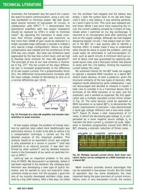
was a multiple cascoded current mirror shown<br />
in Fig. 24. The same devices could be operated as<br />
MOS transistors or as lateral BJT’s, to demonstrate the<br />
drastic improvement in precision. I also demonstrated<br />
a band gap voltage reference and a low-noise amplifier<br />
59 . Figure 25 shows a later measurement of 1/f<br />
noise, in which the decreasing gate voltage V G is compensated<br />
by a more negative source voltage V S to<br />
maintain the drain current I D constant (at 1μA). Operation<br />
is therefore progressively moved from MOS to<br />
BJT, showing a dramatic reduction of flicker noise.<br />
Fig. 24: Multiple cascode current mirror. Each inner concentric<br />
device can be configured as a MOS transistor or as<br />
a lateral BJT.<br />
Weak inversion provides several advantages that<br />
can be exploited in low-power circuits. But this mode<br />
of operation also has some drawbacks, the most<br />
important being the poor precision of current mirrors.<br />
Hence, even in very low-power circuits, the various<br />
18 <strong>IEEE</strong> SSCS NEWS Summer 2008