4 Final Report - Emits - ESA
4 Final Report - Emits - ESA
4 Final Report - Emits - ESA

Create successful ePaper yourself
Turn your PDF publications into a flip-book with our unique Google optimized e-Paper software.
4 <strong>Final</strong><br />
<strong>Report</strong><br />
4.3.3.2 UV-VNIR focal planes<br />
For UV and VNIR spectral bands (from 315 to 1040 nm), silicon semi-conductor is the only material<br />
considered, thanks to its large maturity, its lower cost, its ability to build large format arrays and its low<br />
dark current at ambient temperature. Monolithic CMOS array is preferred to CCD for its good maturity<br />
to build large arrays, its better immunity to GEO harsh radiation environment (as shown by<br />
GOCI/COMS CMOS detector qualification) and because smearing during transfer rules out large CCD<br />
arrays for Earth observation.<br />
Monolithic CMOS imagers manufactured with processes optimised for imaging applications (so-called<br />
“CIS”) look by far as the most promising technology for Geo-Oculus. Indeed, thanks to improved<br />
photodiode processes, CIS arrays are featuring excellent electro-optics performances even for small<br />
pixel pitches. Thinned backside CMOS technology is considered to improve the fill factor and therefore<br />
the detection efficiency. Back-illuminated CMOS are already available in the USA and are being<br />
investigated in Europe, so availability in a 5-year frame is very likely.<br />
Considering only mandatory channels, the spectral range to be covered by the CMOS detector (0.4<br />
0.9 µm) is compatible with a conventional “broadband” detector. When accounting for optional<br />
channels, it is impossible to have a good detection efficiency in the large spectral range to be covered<br />
by the CMOS detector (0.315 to 1.04 µm), so two detectors are used, one optimised for UV & short<br />
visible wavelengths (“UV-blue” detector) and the other for red & NIR wavelength (“Red-NIR” detector).<br />
The largest space CMOS arrays currently available in Europe are in the range of 1.5k x 1.5k pixels<br />
(e.g. COBRA2M 2 Mpixels detector developed by Astrium & ISAE/CIMI for the COMS/GOCI<br />
instrument). The next step will be 3k x 3k arrays, expected for 2010-2011. There is therefore a major<br />
step to be performed in order to reach the typical 100 Mpixel array size required for Geo-Oculus. Even<br />
though there is no strict limitation in CMOS array size, such large arrays set many technical<br />
challenges. In particular, the manufacturing process shall be well mastered to guaranty a sufficient<br />
yield, i.e. a reasonable cost & development schedule. Moreover, to build a very large format array<br />
without dead zone with good electro-optics performances and not to constraint too much the planarity,<br />
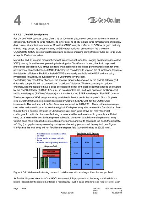
stitching (i.e. gap-less array assembly during manufacturing process) will be required (see Figure<br />
4.3-7) since the total array will not fit within the stepper field (currently limited to 22x22 mm²).<br />
– Sub-blocks are exposed one after<br />
another<br />
– Some blocks are used multiple<br />
times<br />
– Ultimate limit is given by wafer size<br />
22mm<br />
V<br />
1<br />
Stepper field<br />
horiscan2<br />
horiscan1<br />
V V<br />
2 3<br />
array<br />
Stitched CMOS Sensor<br />
horiscan1 horiscan2<br />
array array array<br />
array array array<br />
array array array<br />
Figure 4.3-7: Wafer-level stitching is used to build arrays with size larger than the stepper field<br />
As for the 2 Mpixels detector of the GOCI instrument, it is proposed that the array is divided 4 subblocks<br />
independently operated, offering a redundancy level in case of failure (see Figure 4.3-8). Each<br />
Page 4-34 Doc. No: GOC-ASG-RP-002<br />
Issue: 2<br />
Astrium GmbH Date: 13.05.2009<br />
V<br />
1<br />
V<br />
2<br />
V<br />
3