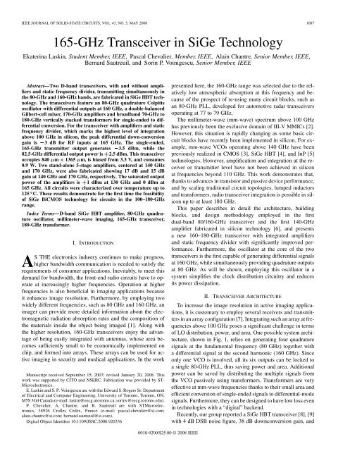
165-GHz Transceiver in SiGe Technology - Computer Engineering ...
165-GHz Transceiver in SiGe Technology - Computer Engineering ...
165-GHz Transceiver in SiGe Technology - Computer Engineering ...
Create successful ePaper yourself
Turn your PDF publications into a flip-book with our unique Google optimized e-Paper software.
IEEE JOURNAL OF SOLID-STATE CIRCUITS, VOL. 43, NO. 5, MAY 2008 1087<br />
<strong>165</strong>-<strong>GHz</strong> <strong>Transceiver</strong> <strong>in</strong> <strong>SiGe</strong> <strong>Technology</strong><br />
Ekater<strong>in</strong>a Lask<strong>in</strong>, Student Member, IEEE, Pascal Chevalier, Member, IEEE, Ala<strong>in</strong> Chantre, Senior Member, IEEE,<br />
Bernard Sautreuil, and Sor<strong>in</strong> P. Vo<strong>in</strong>igescu, Senior Member, IEEE<br />
Abstract—Two D-band transceivers, with and without amplifiers<br />
and static frequency divider, transmitt<strong>in</strong>g simultaneously <strong>in</strong><br />
the 80-<strong>GHz</strong> and 160-<strong>GHz</strong> bands, are fabricated <strong>in</strong> <strong>SiGe</strong> HBT technology.<br />
The transceivers feature an 80-<strong>GHz</strong> quadrature Colpitts<br />
oscillator with differential outputs at 160 <strong>GHz</strong>, a double-balanced<br />
Gilbert-cell mixer, 170-<strong>GHz</strong> amplifiers and broadband 70-<strong>GHz</strong> to<br />
180-<strong>GHz</strong> vertically stacked transformers for s<strong>in</strong>gle-ended to differential<br />
conversion. For the transceiver with amplifiers and static<br />
frequency divider, which marks the highest level of <strong>in</strong>tegration<br />
above 100 <strong>GHz</strong> <strong>in</strong> silicon, the peak differential down-conversion<br />
ga<strong>in</strong> is 3 dB for RF <strong>in</strong>puts at <strong>165</strong> <strong>GHz</strong>. The s<strong>in</strong>gle-ended,<br />
<strong>165</strong>-<strong>GHz</strong> transmitter output generates 3.5 dBm, while the<br />
82.5-<strong>GHz</strong> differential output power is C2.5 dBm. This transceiver<br />
occupies 840 m 1365 m, is biased from 3.3 V, and consumes<br />
0.9 W. Two stand-alone 5-stage amplifiers, centered at 140 <strong>GHz</strong><br />
and 170 <strong>GHz</strong>, were also fabricated show<strong>in</strong>g 17 dB and 15 dB<br />
ga<strong>in</strong> at 140 <strong>GHz</strong> and 170 <strong>GHz</strong>, respectively. The saturated output<br />
power of the amplifiers is C1 dBm at 130 <strong>GHz</strong> and 0 dBm at<br />
<strong>165</strong> <strong>GHz</strong>. All circuits were characterized over temperature up to<br />
125 C. These results demonstrate for the first time the feasibility<br />
of <strong>SiGe</strong> BiCMOS technology for circuits <strong>in</strong> the 100–180-<strong>GHz</strong><br />
range.<br />
Index Terms—D-band <strong>SiGe</strong> HBT amplifier, 80-<strong>GHz</strong> quadrature<br />
oscillator, millimeter-wave imag<strong>in</strong>g, <strong>165</strong>-<strong>GHz</strong> transceiver,<br />
180-<strong>GHz</strong> transformer.<br />
I. INTRODUCTION<br />
AS THE electronics <strong>in</strong>dustry cont<strong>in</strong>ues to make progress,<br />
higher bandwidth communication is needed to satisfy the<br />
requirements of consumer applications. Inevitably, to meet this<br />
demand for bandwidth, the front-end radio circuits have to operate<br />
at <strong>in</strong>creas<strong>in</strong>gly higher frequencies. Operation at higher<br />
frequencies is also beneficial <strong>in</strong> imag<strong>in</strong>g applications because<br />
it enhances image resolution. Furthermore, by employ<strong>in</strong>g two<br />
widely different frequencies, such as 80 <strong>GHz</strong> and 160 <strong>GHz</strong>, an<br />
imager can provide more detailed <strong>in</strong>formation about the electromagnetic<br />
radiation absorption rates and the composition of<br />
the materials <strong>in</strong>side the object be<strong>in</strong>g imaged [1]. Along with<br />
the higher resolution, 160-<strong>GHz</strong> transceivers enjoy the advantage<br />
of be<strong>in</strong>g easily <strong>in</strong>tegrated with antennas, whose area becomes<br />
sufficiently small to be economically implemented on<br />
chip, and formed <strong>in</strong>to arrays. These arrays can be used for active<br />
imag<strong>in</strong>g <strong>in</strong> security and medical applications. In the work<br />
Manuscript received September 15, 2007; revised January 20, 2008. This<br />
work was supported by CITO and NSERC. Fabrication was provided by ST-<br />
Microelectronics.<br />
E. Lask<strong>in</strong> and S. P. Vo<strong>in</strong>igescu are with the Edward S. Rogers Sr. Department<br />
of Electrical and <strong>Computer</strong> Eng<strong>in</strong>eer<strong>in</strong>g, University of Toronto, Toronto, ON,<br />
M5S 3G4 Canada (e-mail: lask<strong>in</strong>@eecg.utoronto.ca; sor<strong>in</strong>v@eecg.toronto.edu).<br />
P. Chevalier, A. Chantre, and B. Sautreuil are with STMicroelectronics,<br />
38926 Crolles Cedex, France (e-mail: pascal.chevalier@st.com;<br />
ala<strong>in</strong>.chantre@st.com; bernard.sautreuil@st.com).<br />
Digital Object Identifier 10.1109/JSSC.2008.920336<br />
0018-9200/$25.00 © 2008 IEEE<br />
presented here, the 160-<strong>GHz</strong> range was selected due to the relatively<br />
low atmospheric absorption at this frequency and because<br />
of the prospect of re-us<strong>in</strong>g many circuit blocks, such as<br />
an 80-<strong>GHz</strong> PLL, developed for automotive radar transceivers<br />
operat<strong>in</strong>g at 77 to 79 <strong>GHz</strong>.<br />
The millimeter-wave (mm-wave) spectrum above 100 <strong>GHz</strong><br />
has previously been the exclusive doma<strong>in</strong> of III-V MMICs [2].<br />
However, this situation is rapidly chang<strong>in</strong>g as some basic circuit<br />
blocks have recently been implemented <strong>in</strong> silicon. For example,<br />
mm-wave VCOs operat<strong>in</strong>g above 140 <strong>GHz</strong> have been<br />
previously realized <strong>in</strong> CMOS [3], <strong>SiGe</strong> HBT [4], and InP [5]<br />
technologies. However, amplification and <strong>in</strong>tegration at the receiver<br />
or transmitter level have not been achieved <strong>in</strong> silicon<br />
at frequencies beyond 110 <strong>GHz</strong>. This work demonstrates that,<br />
thanks to advances <strong>in</strong> transistor and passive device performance,<br />
and by scal<strong>in</strong>g traditional circuit topologies, lumped <strong>in</strong>ductors<br />
and transformers, radio transceiver <strong>in</strong>tegration is possible <strong>in</strong> silicon<br />
up to at least 180 <strong>GHz</strong>.<br />
This paper describes <strong>in</strong> detail the architecture, build<strong>in</strong>g<br />
blocks, and design methodology employed <strong>in</strong> the first<br />
dual-band 80/160-<strong>GHz</strong> transceiver and the first 140-<strong>GHz</strong><br />
amplifier fabricated <strong>in</strong> silicon technology [6], and presents<br />
a new 160–180-<strong>GHz</strong> transceiver with <strong>in</strong>tegrated amplifiers<br />
and static frequency divider with significantly improved performance.<br />
Furthermore, the oscillator at the core of the two<br />
transceivers is the first capable of generat<strong>in</strong>g differential signals<br />
at 160 <strong>GHz</strong>, while simultaneously provid<strong>in</strong>g quadrature outputs<br />
at 80 <strong>GHz</strong>. As will be shown, employ<strong>in</strong>g this oscillator <strong>in</strong> a<br />
system simplifies the clock distribution circuitry and reduces<br />
its power dissipation.<br />
II. TRANSCEIVER ARCHITECTURE<br />
To <strong>in</strong>crease the image resolution <strong>in</strong> active imag<strong>in</strong>g applications,<br />
it is customary to employ several receivers and transmitters<br />
<strong>in</strong> an array configuration [7]. Integrat<strong>in</strong>g such an array at frequencies<br />
above 100 <strong>GHz</strong> poses a significant challenge <strong>in</strong> terms<br />
of LO distribution, power, and area. One possible system architecture,<br />
shown <strong>in</strong> Fig. 1, relies on generat<strong>in</strong>g four quadrature<br />
signals at the fundamental frequency (80 <strong>GHz</strong>) together with<br />
a differential signal at the second harmonic (160 <strong>GHz</strong>). S<strong>in</strong>ce<br />
only one VCO is <strong>in</strong>volved, all its six outputs can be locked to<br />
a s<strong>in</strong>gle 80-<strong>GHz</strong> PLL, thus sav<strong>in</strong>g power and area. Additional<br />
power can be saved by distribut<strong>in</strong>g the multiple signals from<br />
the VCO passively us<strong>in</strong>g transformers. Transformers are very<br />
effective at mm-wave frequencies thanks to their small area and<br />
efficient conversion of s<strong>in</strong>gle-ended signals to differential-mode<br />
signals. Furthermore, they can be designed to have low loss even<br />
<strong>in</strong> technologies with a “digital” backend.<br />
Recently, our group reported a <strong>SiGe</strong> HBT transceiver [8], [9]<br />
with 4 dB DSB noise figure, 38 dB downconversion ga<strong>in</strong>, and
1088 IEEE JOURNAL OF SOLID-STATE CIRCUITS, VOL. 43, NO. 5, MAY 2008<br />
Fig. 1. Dual-frequency transceiver array block diagram.<br />
Fig. 2. Top-level 80/160-<strong>GHz</strong> transceiver schematic (transceiver 1).<br />
dBm output power, that can be employed as the 80-<strong>GHz</strong><br />
part of the system <strong>in</strong> Fig. 1. This paper focuses on the design<br />
of the 160-<strong>GHz</strong> part of the system and describes two transceivers.<br />
The first is a proof-of-concept s<strong>in</strong>gle-chip transceiver<br />
with reduced <strong>in</strong>tegration level, whose schematic is illustrated <strong>in</strong><br />
Fig. 2, and which will be henceforth referred to as transceiver<br />
1 [6]. The second s<strong>in</strong>gle-chip transceiver, referred to as transceiver<br />
2, builds on the first, and also <strong>in</strong>cludes three <strong>165</strong>-<strong>GHz</strong><br />
amplifiers and an 80-<strong>GHz</strong> static frequency divider, as illustrated<br />
<strong>in</strong> Fig. 3. It marks the highest level of <strong>in</strong>tegration <strong>in</strong> silicon<br />
above 100 <strong>GHz</strong>. In this transceiver, the s<strong>in</strong>gle-ended <strong>in</strong>put is<br />
amplified by the receive-amplifier and is converted to a differential<br />
signal by transformer T1 before reach<strong>in</strong>g the mixer. A<br />
differential <strong>165</strong>-<strong>GHz</strong> LO signal is generated us<strong>in</strong>g the 82.5-<strong>GHz</strong><br />
quadrature oscillator. This <strong>165</strong>-<strong>GHz</strong> differential LO is treated as<br />
two s<strong>in</strong>gle-ended signals, each of which is amplified separately.<br />
Transformer T2 connects the amplified LO signal to the mixer,<br />
while the second amplified LO signal is used as the <strong>165</strong>-<strong>GHz</strong><br />
transmitter output. The quadrature oscillator also produces two<br />
differential 82.5-<strong>GHz</strong> signals. One of the 82.5-<strong>GHz</strong> differential<br />
outputs drives the static frequency divider [10], while the other<br />
is term<strong>in</strong>ated with 50- resistors on-chip. However, <strong>in</strong> a future<br />
version of this chip, the latter can also be used to <strong>in</strong>tegrate an<br />
80-<strong>GHz</strong> transceiver on the same die. The mixer, oscillator and<br />
transformers are identical <strong>in</strong> both transceivers.<br />
III. CIRCUIT BUILDING BLOCKS<br />
A. 80-<strong>GHz</strong> Quadrature Oscillator<br />
In this work, we have employed a quadrature oscillator to<br />
demonstrate that such a topology simplifies the LO distribution<br />
among transceiver arrays. However, it should be noted that <strong>in</strong><br />
Fig. 3. Top-level schematic of the <strong>165</strong>-<strong>GHz</strong> transceiver with transmit, receive,<br />
and LO amplifiers and static frequency divider (transceiver 2).<br />
Fig. 4. A model of a quadrature oscillator, composed of two coupled differential<br />
Colpitts oscillators.<br />
the transceiver topologies discussed here, the quadrature phase<br />
relationship between the two 80-<strong>GHz</strong> differential outputs of<br />
the oscillator is not critical for correct operation. In the past,<br />
quadruple-push oscillators were designed for the purpose of<br />
efficiently generat<strong>in</strong>g a fourth-harmonic signal [11] us<strong>in</strong>g delay<br />
l<strong>in</strong>es. By far the most common quadrature oscillator topology<br />
consists of two <strong>in</strong>ter-locked cross-coupled LC oscillators [12].<br />
However, experimental data have shown that differential Colpitts<br />
oscillators exhibit superior performance <strong>in</strong> terms of phase<br />
noise, tun<strong>in</strong>g range, temperature stability, and operation at<br />
mm-wave frequencies [13]–[15]. To date, quadrature Colpitts<br />
oscillators have been implemented by <strong>in</strong>jection lock<strong>in</strong>g two differential<br />
oscillators [16], [17], as opposed to a quadruple-push<br />
oscillator, and at lower frequency than the oscillator presented<br />
here.<br />
Tak<strong>in</strong>g advantage of the Colpitts topology, and expand<strong>in</strong>g on<br />
a 3-push oscillator concept [18], we are propos<strong>in</strong>g the quadrature<br />
oscillator topology illustrated <strong>in</strong> Fig. 4. It consists of two<br />
coupled differential Colpitts oscillators. In each differential oscillator,<br />
a common-mode resistor ensures that its two outputs<br />
are 180 out of phase [19]. By a similar approach, resistor<br />
, common to both differential oscillators, i.e., shared by<br />
all four Colpitts sub-oscillators, will help to establish 90 phase<br />
difference between the two differential halves of the quadrature<br />
oscillator. The common-mode resistors, along with the star-connection<br />
of the tank <strong>in</strong>ductors at node P, ensure that the four oscillator<br />
outputs can be locked <strong>in</strong> quadrature, as will be shown next.<br />
The proposed oscillator can be analyzed us<strong>in</strong>g modal analysis<br />
by extend<strong>in</strong>g the theory previously developed for push-push and<br />
triple-push oscillators [18], [20], and power amplifiers [21], to<br />
a quadruple-push oscillator. Note that, <strong>in</strong> this paper the terms
LASKIN et al.: <strong>165</strong>-GHZ TRANSCEIVER IN SIGE TECHNOLOGY 1089<br />
Fig. 5. (a) Block diagram and port def<strong>in</strong>itions for a quadruple-push oscillator.<br />
(b) Equivalent circuit for one of the sub-oscillators.<br />
TABLE I<br />
EIGENVECTORS AND EIGENVALUES FOR EACH OSCILLATION MODE<br />
“even mode” and “common mode” are used <strong>in</strong>terchangeably to<br />
mean the same th<strong>in</strong>g. Similarly, “odd mode” and “differential<br />
mode” refer to the same circuit condition.<br />
To start the analysis, the oscillator is represented as the fourport<br />
circuit of Fig. 5(a). Each of the four Colpitts circuits, <strong>in</strong>clud<strong>in</strong>g<br />
their common-mode resistors, is modeled as a separate<br />
sub-oscillator. All four sub-oscillators are coupled with a network<br />
that consists of transmission l<strong>in</strong>es and a load resistor .<br />
The voltage, current, and impedance phasors of the 4-push oscillator<br />
topology are related by the follow<strong>in</strong>g matrix equation:<br />
. Tak<strong>in</strong>g <strong>in</strong>to account the symmetries that exist <strong>in</strong><br />
the circuit, i.e., for and<br />
, the matrix equation can be recast as<br />
The eigenvectors and eigenvalues of (1) represent all the oscillation<br />
modes of the circuit. The eigenvalues and eigenvectors<br />
obta<strong>in</strong>ed by solv<strong>in</strong>g (1) are given <strong>in</strong> Table I. In each oscillation<br />
mode (i.e., even, odd, or quadrature), the phases and relative amplitudes<br />
of the signals produced by the sub-oscillators are represented<br />
by the elements of the eigenvector that describes that<br />
mode. For example, the values of and <strong>in</strong> the<br />
odd mode, illustrate that sub-oscillators 1 and 2 produce signals<br />
of equal amplitude which are 180 out of phase. The impedance<br />
seen at the ports of the oscillator <strong>in</strong> a particular mode is given<br />
by the eigenvalue correspond<strong>in</strong>g to that mode.<br />
The quadrature oscillation mode is described by two eigenvectors<br />
which satisfy the equation and, at<br />
(1)<br />
Fig. 6. Equivalent circuit models for each oscillator mode. (a) Even mode.<br />
(b) Odd mode. (c) Quadrature mode.<br />
the same time, comply with the symmetry of the circuit. The<br />
symmetry requires hav<strong>in</strong>g equal-amplitude oscillations <strong>in</strong> all<br />
four sub-circuits. The two eigenvectors are<br />
To establish correct circuit operation, the even- and odd-mode<br />
oscillations must be suppressed and the quadrature oscillation<br />
mode must be amplified. The conditions for quadrature oscillation<br />
can be derived by <strong>in</strong>spect<strong>in</strong>g any of the quarter-circuits<br />
separately. In Fig. 5(b) the quarter-oscillator is modeled as a<br />
s<strong>in</strong>gle-port. Look<strong>in</strong>g to the left, the impedance of the negative<br />
resistance device appears <strong>in</strong> series with , which represents<br />
the comb<strong>in</strong>ation of and , shown earlier <strong>in</strong><br />
Fig. 4. To the right, one sees , which represents the oscillator<br />
tank, <strong>in</strong> series with the load .<br />
The s<strong>in</strong>gle-port sub-oscillator schematic of Fig. 5(b) is redrawn<br />
for each of the oscillation modes <strong>in</strong> Fig. 6, <strong>in</strong>dicat<strong>in</strong>g the<br />
values of the various common-mode resistors seen <strong>in</strong> each case.<br />
Note that both nodes and are common to all four sub-oscillators.<br />
In the quadrature oscillation mode,<br />
because nodes and appear as virtual grounds. In the odd<br />
mode of oscillation, and , because the<br />
resistors cancel <strong>in</strong> differential mode. S<strong>in</strong>ce two waveforms<br />
add <strong>in</strong> phase across and across their values double<br />
<strong>in</strong> the odd mode of oscillation. Similarly, <strong>in</strong> the even oscillation<br />
mode, where all sub-oscillators are <strong>in</strong> phase, the common-mode<br />
resistors at nodes and become and<br />
, respectively.<br />
By writ<strong>in</strong>g the conditions for suppress<strong>in</strong>g even- and<br />
odd-mode, and enhanc<strong>in</strong>g the quadrature-mode oscillations,<br />
and after substitut<strong>in</strong>g the impedances from Fig. 6, the follow<strong>in</strong>g<br />
equations are obta<strong>in</strong>ed:<br />
Even mode:<br />
(2)<br />
(3)
1090 IEEE JOURNAL OF SOLID-STATE CIRCUITS, VOL. 43, NO. 5, MAY 2008<br />
Fig. 7. Quadrature oscillator schematic.<br />
Odd mode:<br />
Quadrature mode:<br />
F<strong>in</strong>ally, (7) describes the quadrature oscillation condition and<br />
is obta<strong>in</strong>ed from <strong>in</strong>equalities (3), (4), and (5) and from (6), where<br />
is the negative resistance of the active device.<br />
It should be noted that, although the roles of and<br />
are not immediately apparent from the model of Fig. 5(a), they<br />
are critical <strong>in</strong> determ<strong>in</strong><strong>in</strong>g the phases of the oscillator outputs<br />
<strong>in</strong> a circuit implementation. S<strong>in</strong>ce the order of the entries of<br />
the quadrature-mode eigenvectors of (2) can be <strong>in</strong>terchanged<br />
without affect<strong>in</strong>g the solution, and are responsible<br />
for establish<strong>in</strong>g the exact phase relationships of the four outputs<br />
(i.e., which output is 0 , which is 90 , etc.). Furthermore,<br />
and help with suppress<strong>in</strong>g the odd and even oscillation<br />
modes by significantly degrad<strong>in</strong>g the of the capacitor <strong>in</strong><br />
Fig. 6(a) and (b).<br />
(4)<br />
(5)<br />
(6)<br />
(7)<br />
Fig. 8. Layout detail of the quadrature oscillator.<br />
Based on the concepts described above, the oscillator shown<br />
<strong>in</strong> Fig. 7 was designed for quadrature operation at a fundamental<br />
frequency of 80 <strong>GHz</strong>. S<strong>in</strong>ce AMOS varactors were not available<br />
<strong>in</strong> this technology, the oscillator was designed to operate<br />
at a constant frequency. However, more recent work <strong>in</strong> CMOS<br />
[15] illustrates that it is straightforward to extend this oscillator<br />
to a voltage-tunable version. In this design, the load resistor<br />
(of Fig. 5(a), where the fourth-harmonic signal is produced, is<br />
implemented with the bias resistors and . Cascode<br />
transistors are employed to adequately isolate the quadrature<br />
outputs from the tank. They also allow comb<strong>in</strong><strong>in</strong>g the two differential<br />
80-<strong>GHz</strong> signals <strong>in</strong>to two second-harmonic signals at<br />
160 <strong>GHz</strong> that are 180 out of phase.<br />
All transistors <strong>in</strong> the oscillator are biased at the peakcurrent<br />
density of 14 mA/ m to obta<strong>in</strong> the maximum output<br />
sw<strong>in</strong>g. Particular attention was paid to the symmetry of the oscillator<br />
layout, both for differential and for quadrature signals,<br />
as is illustrated <strong>in</strong> Fig. 8. The oscillator operates from 3.3 V, and
LASKIN et al.: <strong>165</strong>-GHZ TRANSCEIVER IN SIGE TECHNOLOGY 1091<br />
Fig. 9. Down-converter mixer schematic.<br />
consumes a total of 70 mA. To the best of our knowledge, this is<br />
the first quadrature oscillator at 80 <strong>GHz</strong> and the first differential<br />
oscillator at 160 <strong>GHz</strong> designed <strong>in</strong> a <strong>SiGe</strong> HBT technology.<br />
B. 160-<strong>GHz</strong> Gilbert-Cell Down-Convert Mixer<br />
A double-balanced Gilbert cell topology [22] mixer with<br />
on-chip RF and LO baluns is employed <strong>in</strong> the receiver. Its<br />
schematic is shown <strong>in</strong> Fig. 9. The baluns, described <strong>in</strong> detail <strong>in</strong><br />
the next section, perform s<strong>in</strong>gle-ended to differential conversion.<br />
The bias for the RF diff-pair and for the LO quad is applied<br />
to the center tap of the secondary coil of each transformer.<br />
Inductors are used <strong>in</strong>stead of a current source to achieve<br />
larger voltage headroom, better l<strong>in</strong>earity, and help to match<br />
the RF <strong>in</strong>put to 50 at 160 <strong>GHz</strong>. Series 36-pH <strong>in</strong>ductors are<br />
<strong>in</strong>serted between the collectors of the RF pair transistors and the<br />
emitters of the mix<strong>in</strong>g quad to suppress the second harmonic<br />
(320 <strong>GHz</strong>) of the RF and LO signals over a broad band. The<br />
reactance of the LO and RF <strong>in</strong>puts is tuned out by employ<strong>in</strong>g<br />
shunt capacitors and series <strong>in</strong>ductive transmission l<strong>in</strong>es, which<br />
are part of the <strong>in</strong>terconnect. The mixer schematic <strong>in</strong>cludes<br />
several <strong>in</strong>ductors that model every piece of <strong>in</strong>terconnect l<strong>in</strong>e<br />
<strong>in</strong> the mixer. L<strong>in</strong>es over the silicon substrate are modeled<br />
us<strong>in</strong>g the <strong>in</strong>ductor 2- model, while <strong>in</strong>terconnect that passes<br />
over metal is described as transmission l<strong>in</strong>es. Furthermore,<br />
all metal-to-metal overlap capacitances are extracted us<strong>in</strong>g<br />
ASITIC and are <strong>in</strong>cluded <strong>in</strong> the simulation schematic. They are<br />
not shown here for clarity.<br />
There is no IF amplifier at the mixer output. Instead, the differential<br />
IF output is matched to 50 at each side over a broad<br />
bandwidth (DC to 10 <strong>GHz</strong>) with the help of a network of <strong>in</strong>ductors,<br />
capacitors ( and ) and on-chip 50- resistors. A<br />
Fig. 10. Layout snapshot of the down-converter mixer.<br />
broad IF bandwidth is required for communications at data rates<br />
above 10 Gb/s and for applications such as radio astronomy and<br />
imag<strong>in</strong>g. In each IF match<strong>in</strong>g network two identical <strong>in</strong>ductors,<br />
, are employed <strong>in</strong>stead of a s<strong>in</strong>gle large <strong>in</strong>ductor, to <strong>in</strong>crease<br />
the self-resonance frequency of those <strong>in</strong>ductors beyond 50 <strong>GHz</strong>.<br />
Shunt capacitors tune the impedance to 50 .<br />
The mixer layout (illustrated <strong>in</strong> Fig. 10) is fully symmetric<br />
with respect to the LO-to-RF l<strong>in</strong>e. Symmetry is essential<br />
for proper double-balanced mix<strong>in</strong>g operation, for impedance<br />
match<strong>in</strong>g, and for achiev<strong>in</strong>g high isolation at mm-wave frequencies.<br />
The mixer operates from 3.3 V and consumes 15 mA.<br />
All transistors have the same size ( m, m)<br />
and are biased at the peak- current density of 14 mA/ m .<br />
Thanks to its balanced multiplier structure, this mixer works up<br />
to a record 180 <strong>GHz</strong>.
1092 IEEE JOURNAL OF SOLID-STATE CIRCUITS, VOL. 43, NO. 5, MAY 2008<br />
Fig. 11. Five-stage 140-<strong>GHz</strong> amplifier schematic.<br />
C. 5-Stage D-Band Amplifiers<br />
A tuned, 5-stage 160-<strong>GHz</strong> amplifier was designed at the<br />
same time as transceiver 1 [6]. Its schematic is illustrated <strong>in</strong><br />
Fig. 11. However, s<strong>in</strong>ce the transistor models were extracted<br />
from measurements below 110 <strong>GHz</strong> and on transistors with<br />
different vertical dop<strong>in</strong>g profiles, it was considered risky to<br />
<strong>in</strong>tegrate the amplifier <strong>in</strong> the transceiver. Indeed, although the<br />
160-<strong>GHz</strong> oscillator frequency was with<strong>in</strong> 1%–3% of simulation,<br />
the measured center frequency of the amplifier, which,<br />
unlike that of the oscillator, is sensitive to the transistor capacitances,<br />
was 13% lower, at 140 <strong>GHz</strong>, accentuat<strong>in</strong>g the difficulty<br />
of design<strong>in</strong>g at this frequency. A second amplifier was next<br />
re-tuned to 180 <strong>GHz</strong> and its center frequency was measured<br />
to be 170 <strong>GHz</strong>. Three 170-<strong>GHz</strong> amplifiers were <strong>in</strong>tegrated <strong>in</strong><br />
transceiver 2. Each of the three had different <strong>in</strong>put and/or output<br />
match<strong>in</strong>g networks, depend<strong>in</strong>g on its location <strong>in</strong> the transceiver.<br />
Both amplifiers were designed us<strong>in</strong>g the same methodology,<br />
described next.<br />
The amplifier design beg<strong>in</strong>s at the last stage and steps backwards<br />
towards the <strong>in</strong>put. The bias current and size of transistors<br />
<strong>in</strong> each stage are progressively scaled (<strong>in</strong>creased) from the<br />
<strong>in</strong>put to the output. Interstage match<strong>in</strong>g is employed to maximize<br />
the power ga<strong>in</strong>. The last two stages of the amplifier employ<br />
a common-emitter topology for higher output power, while<br />
the first 3 stages are implemented with cascodes to obta<strong>in</strong> larger<br />
ga<strong>in</strong>. Each of the <strong>in</strong>ductors shown <strong>in</strong> the amplifier schematic<br />
was simulated <strong>in</strong> ASITIC and described by its correspond<strong>in</strong>g<br />
2- equivalent circuit <strong>in</strong> simulation.<br />
The last stage consists of a CE transistor biased at 30 mA to<br />
obta<strong>in</strong> a 2 dBm (0.8 ) signal <strong>in</strong> a 50- load. Due to the<br />
large current that has to flow through this device and its metallization,<br />
it was implemented as two transistors connected <strong>in</strong> parallel,<br />
each with an emitter length of 7.5 m. The pieces of <strong>in</strong>terconnect<br />
lead<strong>in</strong>g to the parallel-connected devices are shown <strong>in</strong><br />
the schematic as 5.18-pH <strong>in</strong>ductors. The load of the fifth stage<br />
is split <strong>in</strong> two to provide space <strong>in</strong> the layout for the load and<br />
for the output match<strong>in</strong>g network. The last stage has an <strong>in</strong>put<br />
impedance of , which is conjugately matched to<br />
the output of the fourth stage. It, too, uses a CE transistor with<br />
<strong>in</strong>ductive load, whose emitter length and bias current are scaled<br />
down by a factor of 2 compared to the last stage, and presents<br />
an impedance of to the third stage.<br />
In each cascode stage, the output match<strong>in</strong>g network consists<br />
of series and shunt <strong>in</strong>ductors, and a series capacitor. The analysis<br />
and design of each of the amplifier stages can be carried out<br />
either <strong>in</strong> the traditional microwave way with the Smith Chart [1],<br />
or analytically, employ<strong>in</strong>g a lumped high-frequency equivalent<br />
circuit for the transistor, which <strong>in</strong>cludes the parasitic emitter and<br />
base resistances and . To improve the accuracy of this<br />
simplified equivalent circuit at mm-wave frequencies, we rely<br />
on the measured or simulated effective cutoff frequency<br />
and transconductance , where .<br />
Note that <strong>in</strong> Fig. 12(a) and (b), the <strong>in</strong>put capacitance of the transistor<br />
or of the cascode stage is described by , and<br />
<strong>in</strong>cludes the Miller effect. The reverse isolation is not captured<br />
by this circuit. However, it rema<strong>in</strong>s very low because<br />
.<br />
When <strong>in</strong>ductive degeneration is used, as <strong>in</strong> the amplifier stage<br />
under consideration, the <strong>in</strong>put impedance can be derived by<br />
look<strong>in</strong>g at the equivalent circuit <strong>in</strong> Fig. 12(b) and is given by<br />
(8)<br />
(9)<br />
(10)<br />
For conjugate match<strong>in</strong>g at the <strong>in</strong>put, first, is chosen such<br />
that the real part of is equal to . Then, a base <strong>in</strong>ductor<br />
is added to cancel the imag<strong>in</strong>ary part of . From (10), its<br />
value must be .<br />
To f<strong>in</strong>d the ga<strong>in</strong> of the stage, its model is redrawn <strong>in</strong> Fig. 12(c)<br />
assum<strong>in</strong>g that it is conjugately matched, so that . The<br />
losses at the output of the amplifier stage, <strong>in</strong>clud<strong>in</strong>g the transistor<br />
and the output match<strong>in</strong>g network, are represented by a<br />
parallel resistor at resonance. The available power ga<strong>in</strong> <strong>in</strong> a<br />
matched load (to ), is given by<br />
(11)
LASKIN et al.: <strong>165</strong>-GHZ TRANSCEIVER IN SIGE TECHNOLOGY 1093<br />
Fig. 12. (a) Transistor small-signal model. (b) Transistor small-signal model<br />
with <strong>in</strong>ductive degeneration. (c) Small-signal model of an amplifier stage.<br />
(d) Impedance transformation us<strong>in</strong>g split <strong>in</strong>ductor load.<br />
To evaluate the accuracy of the hand-design (8)–(11) and of<br />
the simplified equivalent circuit of the transistor, an HBT test<br />
structure with 5.74 m emitter length was measured on the same<br />
wafer with the amplifier. Its extracted small signal model parameters<br />
were scaled for transistors with emitter lengths of 4 m<br />
and 7.5 m and listed <strong>in</strong> Table II. The accuracy of the <strong>in</strong>put capacitance<br />
prediction for a CE stage us<strong>in</strong>g the simplified equivalent<br />
circuit was estimated by compar<strong>in</strong>g the measured<br />
with for the 7.5- m device. Less than 10% error<br />
was found. By substitut<strong>in</strong>g the values of Table II <strong>in</strong>to (10), the<br />
<strong>in</strong>put impedance of stage 3 of the amplifier can be calculated as<br />
at 140 <strong>GHz</strong>. The 16-fF series capacitor<br />
<strong>in</strong> front of stage 3 cancels the imag<strong>in</strong>ary part of this impedance,<br />
thus present<strong>in</strong>g a load of to stage 2. Similarly the<br />
<strong>in</strong>put impedance of stage 2 can be calculated as ,<br />
lead<strong>in</strong>g to for stage 2. The two 27.6-pH <strong>in</strong>ductive<br />
loads of stage 2, along with that consists of transistor<br />
and <strong>in</strong>ductor parasitics, transform to . These<br />
values, together with <strong>GHz</strong> can now be substituted<br />
TABLE II<br />
MEASURED SMALL SIGNAL MODEL PARAMETERS<br />
OF AMPLIFIER TRANSISTORS<br />
<strong>in</strong>to (11) to obta<strong>in</strong> the ga<strong>in</strong> for stage 2 as 4.3 dB. This value is<br />
close to the simulated ga<strong>in</strong> of 3 dB to 4 dB per stage, lead<strong>in</strong>g to<br />
a total ga<strong>in</strong> of 20 dB for the five amplifier stages<br />
(12)<br />
The impedance transformation that occurs <strong>in</strong> the split load<br />
of an amplifier stage can be expla<strong>in</strong>ed by (12), which gives the<br />
impedance look<strong>in</strong>g from the <strong>in</strong>put of a follow<strong>in</strong>g stage towards<br />
the of a preced<strong>in</strong>g stage, as shown <strong>in</strong> Fig. 12(d). From (12)<br />
it is apparent that to cancel the imag<strong>in</strong>ary part of must<br />
be equal to . In this case the real part of becomes<br />
. Thus, by employ<strong>in</strong>g split <strong>in</strong>ductor loads, ,<br />
which is seen at the collector, can be transformed to a much<br />
lower impedance that exists at the <strong>in</strong>put of the next amplifier<br />
stage.<br />
All transistors are biased at the peak- current density of<br />
14 mA/ m . This choice of bias<strong>in</strong>g and transistor siz<strong>in</strong>g helps<br />
to maximize the power transfer between stages because the<br />
of each stage (10) is approximately equal to the of the previous<br />
stage. The imag<strong>in</strong>ary part (which is approximately equal<br />
to 1/3 of the real part) is canceled us<strong>in</strong>g <strong>in</strong>terstage series capacitors<br />
and/or <strong>in</strong>ductors. In a similar manner, the first stage is<br />
matched to 50 by and impedance transformation<br />
<strong>in</strong> the the <strong>in</strong>put match<strong>in</strong>g network.<br />
All bias voltages, supply and ground are distributed on metal<br />
mesh planes with ample substrate contacts everywhere on chip.<br />
The metal mesh adds capacitance between the bias planes<br />
and ground [23]. For additional de-coupl<strong>in</strong>g, MiM capacitors<br />
of 0.5 pF (that are divided <strong>in</strong>to 250-fF capacitors <strong>in</strong> parallel<br />
to avoid resonance) are positioned near each DC node of the<br />
circuit. The amplifier is AC-coupled for simpler test<strong>in</strong>g.<br />
D. Passive Components<br />
1) 1-to-1 160-<strong>GHz</strong> Transformer: Identical transformers<br />
were employed at the RF and LO ports of the mixer for<br />
s<strong>in</strong>gle-ended to differential signal conversion. Passive transformers<br />
are preferred to other methods of s<strong>in</strong>gle-ended to<br />
differential conversion, such as differential pairs, s<strong>in</strong>ce they do<br />
not consume any DC power. Furthermore, due to their symmetry,<br />
transformers have better common mode rejection than<br />
differential pairs at mm-wave frequencies. In this transceiver,
1094 IEEE JOURNAL OF SOLID-STATE CIRCUITS, VOL. 43, NO. 5, MAY 2008<br />
Fig. 13. Transformer 2-% model (left) and transformer geometry (right).<br />
transformers are also used to AC-couple the RF and LO <strong>in</strong>puts<br />
to the mixer because they facilitate bias<strong>in</strong>g of the mixer through<br />
the transformer center tap.<br />
The transformer geometry and its model are shown <strong>in</strong><br />
Fig. 13. The primary and the secondary coils consist of one<br />
square turn with an <strong>in</strong>ner diameter of 20 m and with 2.5 m<br />
metal width. The transformer coils are placed directly above<br />
the silicon substrate, with the top coil implemented <strong>in</strong> the<br />
top alum<strong>in</strong>um (Alucap) layer, and the lower coil <strong>in</strong> Metal 6,<br />
which is made of copper. The top coil has a center tap for<br />
bias<strong>in</strong>g circuits connected to the transformer. The ASITIC<br />
[24] program (version 3.19.00) was employed to simulate the<br />
transformer geometry and to optimize it for lowest loss around<br />
160 <strong>GHz</strong>. A list of ASITIC commands used to def<strong>in</strong>e the<br />
transformer structure is given <strong>in</strong> the Appendix. Because of the<br />
small transformer footpr<strong>in</strong>t, the simulated silicon area below<br />
and around the transformer was reduced to 64 m 64 m<br />
to produce a sufficiently f<strong>in</strong>e grid <strong>in</strong> the metal w<strong>in</strong>d<strong>in</strong>gs, as<br />
required to ensure good accuracy.<br />
A lumped equivalent circuit, consist<strong>in</strong>g of frequency-<strong>in</strong>dependent<br />
circuit elements, was extracted for the transformer<br />
(Fig. 13) and was employed <strong>in</strong> all circuit simulations. It comprises<br />
a 2- model for the coils and 2- models for each of the<br />
short wires connected to the transformer coils. The 2- models<br />
were obta<strong>in</strong>ed by follow<strong>in</strong>g the procedure outl<strong>in</strong>ed <strong>in</strong> [25].<br />
The simulated self-resonance frequency of the transformer is<br />
approximately 400 <strong>GHz</strong>. Fig. 14 compares the transformer<br />
S-parameters simulated with ASITIC, those obta<strong>in</strong>ed with<br />
the 2- model <strong>in</strong> SpectreRF, and the measured and MAG<br />
(essentially the transformer loss) <strong>in</strong> the 1–70-<strong>GHz</strong>, 57–94-<strong>GHz</strong>,<br />
and 116–184-<strong>GHz</strong> frequency ranges. Good agreement of both<br />
and MAG is achieved, with<strong>in</strong> the measurement accuracy.<br />
Although shows a loss of approximately 4 dB, MAG<br />
represents the transformer loss as it is used <strong>in</strong> the circuit, when<br />
all ports are matched. Thus, the true transformer loss is below<br />
2 dB. For measurements below 94 <strong>GHz</strong>, LRM calibration and<br />
T-l<strong>in</strong>e de-embedd<strong>in</strong>g were employed, as described <strong>in</strong> [26].<br />
The scatter <strong>in</strong> the measured and data is due to the<br />
difficulty of accurately measur<strong>in</strong>g and de-embedd<strong>in</strong>g parasitic<br />
capacitances (below 1 fF), resistances (below 0.1 ) and <strong>in</strong>ductances<br />
(below 1 pH). For example, errors or uncerta<strong>in</strong>ty <strong>in</strong><br />
the probe-pad contact resistance of 0.1 , parasitic <strong>in</strong>ductance<br />
of 1 pH, and error <strong>in</strong> pad capacitance of 2 fF, can change the<br />
measured , and by as much as 1 dB <strong>in</strong> either<br />
direction for the small <strong>in</strong>ductors and transformers discussed<br />
Fig. 14. Comparison of transformer ƒ ƒ ƒ and MAG simulated us<strong>in</strong>g<br />
ASITIC (open circles), modeled with 2-% model <strong>in</strong> SpectreRF (l<strong>in</strong>es), and measured<br />
<strong>in</strong> three frequency ranges (dots) us<strong>in</strong>g two VNAs and power <strong>in</strong>sertion loss<br />
measurements beyond 110 <strong>GHz</strong>.<br />
<strong>in</strong> this paper. Above 100 <strong>GHz</strong>, the transmission loss<br />
of the transformer was measured us<strong>in</strong>g a scalar transmission<br />
measurement as described <strong>in</strong> Section V.<br />
2) 50-pH Oscillator Tank Inductor: To m<strong>in</strong>imize the phase<br />
noise of the Colpitts oscillator, the quality factor of the<br />
tank must be maximized. For this purpose, the loss of the tank<br />
<strong>in</strong>ductor was reduced by implement<strong>in</strong>g the <strong>in</strong>ductor coil with<br />
two metals shunted together (Alucap and Metal 6), and with<br />
a Metal 5 underpass (Fig. 15). An <strong>in</strong>ductor geometry with<br />
2.8- m metal width, 2- m spac<strong>in</strong>g, and an <strong>in</strong>ner diameter of<br />
9 m was chosen to push the self-resonance frequency above<br />
400 <strong>GHz</strong>. The <strong>in</strong>ductor coil was placed directly over the silicon<br />
substrate, without any polysilicon or metal shield. Microstrip<br />
transmission l<strong>in</strong>es (3.6- m-wide Metal 6 signal l<strong>in</strong>e over Metal<br />
1 and Metal 2 ground plane) were employed to symmetrically<br />
connect the four tank <strong>in</strong>ductors of the oscillator together.<br />
Just as <strong>in</strong> the transformer case, a 2- model was extracted<br />
from the ASITIC simulated Y-parameters, as shown <strong>in</strong> Fig. 15.<br />
Fig. 16 compares the measured L, R and effective of<br />
the <strong>in</strong>ductor to those simulated us<strong>in</strong>g ASITIC and modeled<br />
with the 2- model. The measurement was performed<br />
us<strong>in</strong>g two network analyzers cover<strong>in</strong>g the 1–70-<strong>GHz</strong> and<br />
the 57–94-<strong>GHz</strong> frequency ranges. Effective is def<strong>in</strong>ed as<br />
. The measured <strong>in</strong>ductance value<br />
<strong>in</strong>creases below 10 <strong>GHz</strong> due to imperfect probes and contact<br />
resistance. Except for the scatter <strong>in</strong> the measured data <strong>in</strong> the
LASKIN et al.: <strong>165</strong>-GHZ TRANSCEIVER IN SIGE TECHNOLOGY 1095<br />
Fig. 15. Inductor 2-% model (left) and <strong>in</strong>ductor geometry (right).<br />
Fig. 16. Comparison of <strong>in</strong>ductor L, R, and simulated us<strong>in</strong>g ASITIC, modeled<br />
with 2-% model, and measured over two frequency ranges us<strong>in</strong>g two different<br />
VNAs.<br />
57–94-<strong>GHz</strong> range due to the difficulty of measur<strong>in</strong>g resistance<br />
with less than 0.1- accuracy, the agreement between simulations<br />
and measurements is very good.<br />
IV. FABRICATION<br />
<strong>Transceiver</strong> 1 (Fig. 2) and the 140-<strong>GHz</strong> amplifier were<br />
fabricated <strong>in</strong> a <strong>SiGe</strong> HBT technology with nom<strong>in</strong>al of<br />
300 <strong>GHz</strong> and of 230 <strong>GHz</strong> [27]. <strong>Transceiver</strong> 2 (Fig. 3) and<br />
the 170-<strong>GHz</strong> amplifier were fabricated <strong>in</strong> a different run of the<br />
<strong>SiGe</strong> HBT technology, with the same backend, but where the<br />
was 340 <strong>GHz</strong> and was 270 <strong>GHz</strong>. The measured<br />
and curves for a nom<strong>in</strong>al device <strong>in</strong> each run are shown <strong>in</strong><br />
Fig. 17. S<strong>in</strong>ce the technology is still under development, the<br />
140-<strong>GHz</strong> amplifier was also fabricated <strong>in</strong> several different<br />
process splits where the HBT profile was <strong>in</strong>tentionally varied,<br />
to determ<strong>in</strong>e which structure results <strong>in</strong> the best circuit performance<br />
at frequencies above 100 <strong>GHz</strong>. The wafer splits cover<br />
<strong>SiGe</strong> HBTs with values which vary <strong>in</strong> a correlated<br />
manner between 230/240 <strong>GHz</strong> and 280/290 <strong>GHz</strong>, respectively.<br />
The collector dop<strong>in</strong>g, the emitter width, or the emitter-base<br />
junction parameters were <strong>in</strong>tentionally modified from wafer to<br />
wafer <strong>in</strong> order to produce the and variations. The rest<br />
of the <strong>SiGe</strong> BiCMOS process steps are identical for all wafer<br />
splits.<br />
The process features a digital CMOS backend with 6 copper<br />
layers and a regular thickness, top alum<strong>in</strong>um metal layer.<br />
MiM capacitors and polysilicon resistors are also available.<br />
Fig. 17. Plot of measured � and � versus current density. The two sets<br />
of curves correspond to two different fab runs: the 140-<strong>GHz</strong> amplifier and transceiver<br />
1 were fabricated <strong>in</strong> the first run. The 170-<strong>GHz</strong> amplifier and transceiver<br />
2 were fabricated <strong>in</strong> the second run.<br />
Fig. 18. Die photo of transceiver 1. The total area <strong>in</strong>clud<strong>in</strong>g pads is<br />
650 "m2 700 "m.<br />
Die photos of transceiver 1 and transceiver 2 are reproduced<br />
<strong>in</strong> Figs. 18 and 19, respectively. A die photo of the 140-<strong>GHz</strong><br />
amplifier is illustrated <strong>in</strong> Fig. 20.<br />
V. MEASUREMENT RESULTS<br />
Measurements were conducted on wafer us<strong>in</strong>g 110–170-<strong>GHz</strong><br />
waveguide probes. A 110–170-<strong>GHz</strong> OLM 12 multiplier<br />
signal source, an Agilent E4448A power spectrum analyzer<br />
(PSA) <strong>in</strong> conjunction with a Farran 110–170-<strong>GHz</strong> down-convert<br />
mixer, and an ELVA 110–170-<strong>GHz</strong> power sensor were<br />
employed for signal generation, spectral, and power measurements.<br />
The setup with power sensor is illustrated <strong>in</strong> Fig. 21.<br />
A 0–30-dB variable attenuator was used <strong>in</strong> the l<strong>in</strong>earity<br />
measurements.<br />
S<strong>in</strong>ce no network analyzer was available <strong>in</strong> the 110–170-<strong>GHz</strong><br />
range, the amplifier ga<strong>in</strong> and the transformer loss ( <strong>in</strong><br />
Fig. 14) <strong>in</strong> this frequency band were obta<strong>in</strong>ed with transmission<br />
measurements by follow<strong>in</strong>g a two-step procedure. In the first<br />
step a signal source was connected to the DUT (amplifier or<br />
transformer) <strong>in</strong>put and either the spectrum analyzer or the<br />
power sensor was connected at the output. The output power
1096 IEEE JOURNAL OF SOLID-STATE CIRCUITS, VOL. 43, NO. 5, MAY 2008<br />
Fig. 19. Die photo of transceiver 2 with <strong>in</strong>tegrated amplifiers and static frequency<br />
divider. The total area <strong>in</strong>clud<strong>in</strong>g pads is 840 "m21365 "m.<br />
Fig. 20. Die photo of the 140-<strong>GHz</strong>. The active circuit area is 200 "m2<br />
400 "m.<br />
Fig. 21. On-wafer 160-<strong>GHz</strong> test setup for transmitter output power measurements<br />
show<strong>in</strong>g the signal source on the left, applied at the receiver <strong>in</strong>put<br />
through 110–170-<strong>GHz</strong> waveguide probes. The 110–170-<strong>GHz</strong> power sensor is<br />
at the right. The IF output is collected at the bottom with differential probes.<br />
was recorded at each frequency. In the second step, the output<br />
power was recorded aga<strong>in</strong>, after replac<strong>in</strong>g the DUT by a “thru”<br />
located on a standard 110-<strong>GHz</strong> Cascade Microtech calibration<br />
Fig. 22. Measured ga<strong>in</strong> (symbols) at 25 C of the 140-<strong>GHz</strong> amplifier and the<br />
170-<strong>GHz</strong> amplifier. Simulated S-parameters (l<strong>in</strong>es) of the 170-<strong>GHz</strong> amplifier.<br />
substrate and keep<strong>in</strong>g the rest of the setup unchanged. The<br />
power measured with the “thru” was subtracted from the power<br />
measured with the DUT <strong>in</strong> place to obta<strong>in</strong> the ga<strong>in</strong>. Thus, all<br />
power ga<strong>in</strong> measurements <strong>in</strong>clude the on-wafer pads, which<br />
have not been de-embedded.<br />
A. D-Band Amplifiers<br />
The measured ga<strong>in</strong>s of the 140-<strong>GHz</strong> amplifier and the<br />
170-<strong>GHz</strong> amplifier at 25 C are reproduced <strong>in</strong> Fig. 22. For the<br />
140-<strong>GHz</strong> amplifier, the ga<strong>in</strong> rema<strong>in</strong>s above 15 dB from 126<br />
to 144 <strong>GHz</strong>. The measured ga<strong>in</strong> of the 170-<strong>GHz</strong> amplifier is<br />
15 dB, with 3-dB bandwidth from 164 to 175 <strong>GHz</strong>. Fig. 22 also<br />
<strong>in</strong>cludes the simulated S-parameters of the 170-<strong>GHz</strong> amplifier.<br />
There is less than 7% reduction <strong>in</strong> the center frequency between<br />
measurements and simulation, which may be expla<strong>in</strong>ed by the<br />
fact that the technology employed is still under development<br />
[27] and the models, which were extracted from S-parameter<br />
measurements below 110 <strong>GHz</strong>, do not reflect current device<br />
performance accurately. The of the amplifiers could not<br />
be measured due to <strong>in</strong>sufficient sensitivity <strong>in</strong> the measurement<br />
setup.<br />
Fig. 23 reproduces the measured ga<strong>in</strong> of the 140-<strong>GHz</strong> amplifier<br />
as a function of temperature. At 140 <strong>GHz</strong>, the ga<strong>in</strong> decreases<br />
from 17 dB at 25 C to 4 dB at 125 C while <strong>in</strong> the<br />
125–135-<strong>GHz</strong> range it rema<strong>in</strong>s above 10 dB for all temperatures.<br />
The ga<strong>in</strong> variation is small at the lower end and <strong>in</strong>creases<br />
at the upper end of the bandwidth, where the effect of temperature<br />
and process variation is more pronounced. This behavior is<br />
similar to that observed <strong>in</strong> tuned <strong>SiGe</strong> HBT and CMOS amplifiers<br />
operat<strong>in</strong>g at 80 and 60 <strong>GHz</strong>. The power ga<strong>in</strong> at the higher<br />
frequencies depends on the transistor and on the of<br />
the load <strong>in</strong>ductor, and rapidly degrades with <strong>in</strong>creas<strong>in</strong>g temperature,<br />
whereas, at the lower end of the amplifier bandwidth, the<br />
ga<strong>in</strong> is primarily controlled by the ratio of the collector load and<br />
emitter degeneration <strong>in</strong>ductors.<br />
To correlate the effect of the HBT and with the<br />
amplifier performance, several wafer splits were selected where<br />
only one HBT profile parameter, the collector dop<strong>in</strong>g, is varied.<br />
The and of devices <strong>in</strong> those splits, which have opposite<br />
trends, are plotted versus the relative collector dop<strong>in</strong>g <strong>in</strong>
LASKIN et al.: <strong>165</strong>-GHZ TRANSCEIVER IN SIGE TECHNOLOGY 1097<br />
Fig. 23. 140-<strong>GHz</strong> amplifier ga<strong>in</strong> over temperature measured us<strong>in</strong>g a D-band<br />
power sensor.<br />
Fig. 24. Measured � � , and amplifier ga<strong>in</strong> at 130, 135, and 140 <strong>GHz</strong><br />
plotted for four process splits where only the HBT collector dop<strong>in</strong>g is varied.<br />
Fig. 24, along with 140-<strong>GHz</strong> amplifier power ga<strong>in</strong> at three frequencies,<br />
130, 135, and 140 <strong>GHz</strong>. As can be observed, the amplifier<br />
ga<strong>in</strong> and the are both decreas<strong>in</strong>g with <strong>in</strong>creas<strong>in</strong>g<br />
collector dop<strong>in</strong>g, thus the ga<strong>in</strong> is correlated with the of<br />
the <strong>SiGe</strong> HBT, but not with the .<br />
L<strong>in</strong>earity measurements were conducted us<strong>in</strong>g a 12 multiplier<br />
signal source, a 0–30 dB D-band attenuator, and a<br />
D-band power sensor. The power sensor allows measurements<br />
of absolute power that are necessary for obta<strong>in</strong><strong>in</strong>g the P .<br />
The l<strong>in</strong>earity measurements for both amplifiers are illustrated<br />
<strong>in</strong> Fig. 25. The measured <strong>in</strong>put P is 17 dBm and the<br />
saturated output power is 1 dBm at 130 <strong>GHz</strong> for the 140-<strong>GHz</strong><br />
amplifier. The 170-<strong>GHz</strong> amplifier achieves an <strong>in</strong>put P of<br />
18 dBm and saturated output power of 0 dBm at <strong>165</strong> <strong>GHz</strong>.<br />
B. <strong>Transceiver</strong>s<br />
The close-<strong>in</strong> spectrum for phase-noise measurement of transceiver<br />
1 at the 80-<strong>GHz</strong> transmitter output is shown <strong>in</strong> Fig. 26.<br />
The measured power difference is dB at 10 MHz offset<br />
with respect to the carrier. S<strong>in</strong>ce this measurement was made<br />
with 1 MHz resolution bandwidth, the result<strong>in</strong>g phase noise is<br />
less than dBc/Hz at 10 MHz offset. This phase noise is<br />
Fig. 25. Measured l<strong>in</strong>earity of the 140-<strong>GHz</strong> amplifier at 130 <strong>GHz</strong> and measured<br />
l<strong>in</strong>earity of the 170-<strong>GHz</strong> amplifier at <strong>165</strong> <strong>GHz</strong>.<br />
Fig. 26. Measured phase noise of transceiver 1 at the 80-<strong>GHz</strong> transmitter<br />
output.<br />
larger than what was demonstrated previously <strong>in</strong> this technology<br />
[23]. The degradation can be attributed to the quadrature operation<br />
of the oscillator, where the sub-circuits affect each other’s<br />
phase, thus <strong>in</strong>creas<strong>in</strong>g the phase noise [20].<br />
The signal power and frequency at the 160-<strong>GHz</strong> transmitter<br />
outputs of both transceivers are plotted <strong>in</strong> Fig. 27 as a function<br />
of the oscillator supply voltage. After de-embedd<strong>in</strong>g cable and<br />
probe losses, the s<strong>in</strong>gle-ended transmitted power of transceiver<br />
1is 10 dBm at 160 <strong>GHz</strong>. <strong>Transceiver</strong> 2 achieves a maximum<br />
output power of 3.5 dBm at <strong>165</strong> <strong>GHz</strong>.<br />
The measured differential down-conversion receiver ga<strong>in</strong> <strong>in</strong><br />
the 160-<strong>GHz</strong> band is shown <strong>in</strong> Fig. 28 for both transceivers at<br />
25 C. All receiver down-conversion measurements were done<br />
with a fixed LO signal by sweep<strong>in</strong>g the RF. The measurements<br />
were performed with a spectrum analyzer and de-embedded<br />
by subtract<strong>in</strong>g the cable and probe losses from the measured<br />
<strong>in</strong>put RF power and output IF power. The circuit pads were not<br />
de-embedded. The conversion ga<strong>in</strong> of transceiver 1 is 24 dB,<br />
with 13-<strong>GHz</strong> bandwidth. The ga<strong>in</strong> is low due to <strong>in</strong>sufficient LO<br />
power produced by the oscillator <strong>in</strong> transceiver 1. For transceiver<br />
2 the ga<strong>in</strong> <strong>in</strong> the 160-<strong>GHz</strong> band is improved to 3 dB,
1098 IEEE JOURNAL OF SOLID-STATE CIRCUITS, VOL. 43, NO. 5, MAY 2008<br />
Fig. 27. S<strong>in</strong>gle-ended power and frequency at the 160-<strong>GHz</strong> transmitter outputs<br />
of transceiver 1 (filled symbols) and transceiver 2 (open symbols) versus the<br />
oscillator power supply voltage.<br />
Fig. 28. Measured differential down-conversion ga<strong>in</strong> of the receivers <strong>in</strong> transceiver<br />
1 and transceiver 2 at 25 C.<br />
thanks to the <strong>in</strong>tegrated 170-<strong>GHz</strong> amplifiers. However more amplification<br />
of the LO might be needed to br<strong>in</strong>g the LO power at<br />
the mixer to the optimal 0-dBm to 2-dBm level. Even though<br />
the mixer is the same <strong>in</strong> both transceivers, the 3-dB bandwidth<br />
of transceiver 2 is limited to 9 <strong>GHz</strong> by the RF amplifier. Note<br />
that IF amplifiers are not <strong>in</strong>tegrated on-chip, thus all the ga<strong>in</strong> is<br />
achieved at the RF frequency of 160 <strong>GHz</strong>.<br />
The receiver ga<strong>in</strong> of transceiver 2 is summarized <strong>in</strong> Fig. 29<br />
as a function of temperature. The ga<strong>in</strong> is reduced to 11 dB at<br />
75 C, and to 25 dB at 125 C, but the transceiver is still functional.<br />
Fig. 30 illustrates the receiver l<strong>in</strong>earity of transceiver 2<br />
from 25 C to 125 C. At 25 C, the <strong>in</strong>put dB of the receiver<br />
is 20 dBm. The l<strong>in</strong>earity, like the receiver ga<strong>in</strong>, degrades significantly<br />
above 100 C.<br />
The measured total DC power consumption of the <strong>165</strong>-<strong>GHz</strong><br />
transceiver with amplifiers and divider is 0.9 W. Out of that,<br />
340 mW are consumed by the oscillator, 100 mW by the static<br />
frequency divider and its output buffer, 32 mW are dissipated<br />
by the mixer, and each of the amplifiers requires 145 mW.<br />
The performance of both transceivers, the 140-<strong>GHz</strong> amplifier,<br />
and the 170-<strong>GHz</strong> amplifier is summarized <strong>in</strong> Table III.<br />
Fig. 29. Measured differential down-conversion receiver ga<strong>in</strong> of transceiver 2<br />
versus temperature.<br />
Fig. 30. Measured l<strong>in</strong>earity at 168 <strong>GHz</strong> of transceiver 2.<br />
TABLE III<br />
SUMMARY OF SIMULATION AND MEASUREMENT RESULTS FOR THE<br />
TRANSCEIVERS AND AMPLIFIERS<br />
VI. CONCLUSION<br />
This paper is the first to report highly <strong>in</strong>tegrated radio<br />
transceivers <strong>in</strong> silicon at frequencies above 100 <strong>GHz</strong>. Most<br />
importantly, good performance is achieved up to 180 <strong>GHz</strong>,<br />
a factor of two larger than <strong>in</strong> any other silicon transceiver of
LASKIN et al.: <strong>165</strong>-GHZ TRANSCEIVER IN SIGE TECHNOLOGY 1099<br />
comparable complexity, us<strong>in</strong>g design methodologies, circuit<br />
topologies, lumped <strong>in</strong>ductors and transformers commonly<br />
employed below 10 <strong>GHz</strong>. Two 160-<strong>GHz</strong> transceivers and two<br />
stand-alone D-band amplifiers were designed and fabricated.<br />
The first transceiver, which consists of an 80-<strong>GHz</strong> quadrature<br />
oscillator with differential 160-<strong>GHz</strong> outputs, 160-<strong>GHz</strong><br />
Gilbert-cell mixer, and 70–180-<strong>GHz</strong> transformers, proved the<br />
feasibility of a push-push differential oscillator capable of<br />
driv<strong>in</strong>g a double-balanced mixer differentially at 160 <strong>GHz</strong><br />
while simultaneously transmitt<strong>in</strong>g at 80 and 160 <strong>GHz</strong>. The<br />
second transceiver employs the same oscillator and mixer, but<br />
also <strong>in</strong>cludes 170-<strong>GHz</strong> amplifiers on the receive, transmit, and<br />
LO paths, and a static frequency divider. The D-band amplifiers<br />
<strong>in</strong>creased the downconversion ga<strong>in</strong> and transmitter output<br />
power of the second transceiver from 23.5 dB to 3 dB, and<br />
from 10 dBm to 3.5 dBm, respectively, when compared to<br />
the transceiver without amplifiers. Furthermore, its oscillator<br />
simultaneously drives two amplifiers at <strong>165</strong> <strong>GHz</strong> and a static<br />
frequency divider at 82.5 <strong>GHz</strong>, demonstrat<strong>in</strong>g an efficient<br />
solution to the LO distribution problem <strong>in</strong> 80+ <strong>GHz</strong> transceiver<br />
arrays. The Gilbert-cell mixer, the stand-alone amplifiers at 140<br />
and 170 <strong>GHz</strong> with 17 and 15 dB ga<strong>in</strong>, respectively, achieve<br />
record performance for silicon mixers and amplifiers. The<br />
circuits presented <strong>in</strong> this paper pave the way for future SoCs<br />
operat<strong>in</strong>g <strong>in</strong> the 100–200-<strong>GHz</strong> range.<br />
APPENDIX<br />
The follow<strong>in</strong>g code snippet gives the sequence of ASITIC<br />
commands that def<strong>in</strong>e the transformer geometry.<br />
ACKNOWLEDGMENT<br />
The authors wish to acknowledge CMC and J. Pristupa for<br />
CAD support, K. Yau for transistor measurement, and ECTI,<br />
OIT, CFI, and NSERC for fund<strong>in</strong>g.<br />
REFERENCES<br />
[1] D. M. Pozar, Microwave Eng<strong>in</strong>eer<strong>in</strong>g, 3rd ed. New York: Wiley,<br />
2005.<br />
[2] T. Kosugi, M. Tokumitsu, K. Murata, T. Enoki, H. Takahashi, A. Hirata,<br />
and T. Nagatsuma, “120-<strong>GHz</strong> TX/RX waveguide modules for<br />
10-Gbit/s wireless l<strong>in</strong>k system,” <strong>in</strong> 2006 IEEE Compound Semicond.<br />
Integrated Circuit Symp., San Antonio, TX, Nov. 2006, pp. 25–28.<br />
[3] K. K. O, C. Cao, E.-Y. Seok, and S. Sankaran, “CMOS millimeterwave<br />
signal sources and detectors,” <strong>in</strong> IEEE Int. Symp. Circuits Syst.,<br />
New Orleans, LA, May 2007, pp. 2614–2617.<br />
[4] P. Roux, Y. Baeyens, O. Wohlgemuth, and Y. Chen, “A monolithic<br />
<strong>in</strong>tegrated 180 <strong>GHz</strong> <strong>SiGe</strong> HBT push-push oscillator,” <strong>in</strong> 2005 13th<br />
Eur. Gallium Arsenide Other Compound Semicond. Application Symp.,<br />
Paris, France, Oct. 2005, pp. 341–343.<br />
[5] Y. Baeyens, N. Weimann, V. Houtsma, J. We<strong>in</strong>er, Y. Yang, J. Frackoviak,<br />
A. Tate, and Y. K. Chen, “High-power submicron InP D-HBT<br />
push-push oscillators operat<strong>in</strong>g up to 215 <strong>GHz</strong>,” <strong>in</strong> IEEE Compound<br />
Semicond. Integr. Circuit Symp. Dig., Oct. 2005, pp. 208–211.<br />
[6] E. Lask<strong>in</strong>, P. Chevalier, A. Chantre, B. Sautreuil, and S. Vo<strong>in</strong>igescu,<br />
“80/160-<strong>GHz</strong> transceiver and 140-<strong>GHz</strong> amplifier <strong>in</strong> <strong>SiGe</strong> technology,”<br />
<strong>in</strong> 2007 IEEE Radio Frequency Integrated Circuits (RFIC) Symp., Honolulu,<br />
HI, Jun. 2007, pp. 153–156.<br />
[7] S. P. Vo<strong>in</strong>igescu, S. T. Nicolson, M. Khanpour, K. Tang, K. H. K. Yau,<br />
N. Seyed-fathi, A. Timonov, A. Nachman, G. Eleftheriades, P. Schvan,<br />
and M. Yang, “CMOS SOCs at 100 <strong>GHz</strong>: System architectures, device<br />
characterization, and IC design examples,” <strong>in</strong> Proc. IEEE Int. Symp.<br />
Circuits Syst., New Orleans, LA, May 2007, pp. 1971–1974.<br />
[8] S. T. Nicolson, E. Lask<strong>in</strong>, M. Khanpour, R. Aroca, A. Tomk<strong>in</strong>s, K.<br />
H. K. Yau, P. Chevalier, P. Garcia, A. Chantre, B. Sautreuil, and S. P.<br />
Vo<strong>in</strong>igescu, “Design and model<strong>in</strong>g considerations for fully-<strong>in</strong>tegrated<br />
silicon W-band transceivers,” <strong>in</strong> RFIT Workshop Dig., S<strong>in</strong>gapore, 2007,<br />
pp. 141–149.<br />
[9] S. T. Nicolson, P. Chevalier, A. Chantre, B. Sautreuil, and S. P.<br />
Vo<strong>in</strong>igescu, “A 77–79 <strong>GHz</strong> doppler radar transceiver <strong>in</strong> silicon,” <strong>in</strong><br />
IEEE Compound Semicond. Integrated Circuits Symp. Tech. Dig.,<br />
Portland, OR, 2007, pp. 252–255.<br />
[10] E. Lask<strong>in</strong>, S. T. Nicolson, P. Chevalier, A. Chantre, B. Sautreuil, and<br />
S. P. Vo<strong>in</strong>igescu, “Low-power, low-phase noise <strong>SiGe</strong> HBT static frequency<br />
divider topologies up to 100 <strong>GHz</strong>,” <strong>in</strong> Proc. Bipolar/BiCMOS<br />
Circuits Technol. Meet<strong>in</strong>g, Maastricht, Holland, Oct. 2006, pp.<br />
235–238.<br />
[11] H. Xiao, T. Tanaka, and M. Aikawa, “A Ka-band quadruple-push oscillator,”<br />
<strong>in</strong> IEEE MTT-S Int. Microwave Symp. (IMS 2003), Philadelphia,<br />
PA, 2003, vol. 2, pp. 889–892.<br />
[12] B. Razavi, Design of Analog CMOS Integrated Circuits. New York:<br />
McGraw-Hill, 2001.<br />
[13] K. W. Tang, S. Leung, N. Tieu, P. Schvan, and S. P. Vo<strong>in</strong>igescu, “Frequency<br />
scal<strong>in</strong>g and topology comparison of millimeter-wave CMOS<br />
vcos,” <strong>in</strong> 2006 IEEE Compound Semicond. Integrated Circuit Symp.,<br />
San Antonio, TX, Nov. 2006, pp. 55–58.<br />
[14] C. Lee, T. Yao, A. Mangan, K. Yau, M. A. Copeland, and S. P.<br />
Vo<strong>in</strong>igescu, “<strong>SiGe</strong> BiCMOS 65-<strong>GHz</strong> BPSK transmitter and 30 to<br />
122 <strong>GHz</strong> LC-varactor VCOs with up to 21% tun<strong>in</strong>g range,” <strong>in</strong> IEEE<br />
Compound Semicond. Integrated Circuits Symp. Tech. Dig., Monterey,<br />
CA, 2004, pp. 179–1118.<br />
[15] E. Lask<strong>in</strong>, M. Khanpour, R. Aroca, K. W. Tang, P. Garcia, and S. P.<br />
Vo<strong>in</strong>igescu, “95 <strong>GHz</strong> receiver with fundamental frequency VCO and<br />
static frequency divider <strong>in</strong> 65 nm digital CMOS,” <strong>in</strong> IEEE ISSCC Dig.<br />
Tech. Papers, San Francisco, CA, 2008.<br />
[16] X. Li, S. Shekhar, and D. J. Allstot, “G -boosted common-gate LNA<br />
and differential Colpitts VCO/QVCO <strong>in</strong> 0.18-"m CMOS,” IEEE J.<br />
Solid-State Circuits, vol. 40, no. 12, pp. 2609–2619, Dec. 2005.<br />
[17] M. A. T. Sanduleanu and E. Stikvoort, “Highly l<strong>in</strong>ear, varactorless, 24<br />
<strong>GHz</strong> IQ oscillator,” <strong>in</strong> Proc. RFIC Symp., 2005, pp. 577–580.<br />
[18] Y.-L. Tang and H. Wang, “Triple-push oscillator approach: Theory<br />
and experiments,” IEEE J. Solid-State Circuits, vol. 36, no. 10, pp.<br />
1472–1479, Oct. 2001.<br />
[19] L. Dauph<strong>in</strong>ee, M. Copeland, and P. Schvan, “A balanced 1.5 <strong>GHz</strong><br />
voltage controlled oscillator with an <strong>in</strong>tegrated IC resonator,” <strong>in</strong> IEEE<br />
ISSCC Dig. Tech. Papers, San Francisco, CA, 1997, pp. 390–391, 491.<br />
[20] U. L. Rohde, A. K. Poddar, and G. Bock, The Design of Modern Microwave<br />
Oscillators For Wireless Applications. Hoboken, NJ: Wiley,<br />
2005.<br />
[21] R. G. Freitag, “A unified analysis of MMIC power amplifier stability,”<br />
<strong>in</strong> 1992 IEEE Microwave Symp. Dig. MTT-S, Albuquerque, NM, 1992,<br />
pp. 297–300.<br />
[22] B. Gilbert, “A precise four-quadrant multiplier with subnanosecond<br />
response,” IEEE J. Solid-State Circuits, vol. SC-3, no. 4, pp. 365–373,<br />
Dec. 1968.<br />
[23] S. T. Nicolson, K. Yau, P. Chevalier, A. Chantre, B. Sautreuil, K. Tang,<br />
and S. Vo<strong>in</strong>igescu, “Design and scal<strong>in</strong>g of W-band <strong>SiGe</strong> BiCMOS<br />
VCOs,” IEEE J. Solid-State Circuits, vol. 42, no. 9, pp. 1821–1833,<br />
Sep. 2007.<br />
[24] ASITIC. [Onl<strong>in</strong>e]. Available: http://rfic.eecs.berkeley.edu/niknejad/<br />
asitic.html<br />
[25] T. O. Dickson, M.-A. LaCroix, S. Boret, D. Gloria, R. Beerkens,<br />
and S. P. Vo<strong>in</strong>igescu, “30–100-<strong>GHz</strong> <strong>in</strong>ductors and transformers for<br />
millimeter-wave (Bi)CMOS <strong>in</strong>tegrated circuits,” IEEE Trans. Microw.<br />
Theory Tech., vol. 53, no. 1, pp. 123–133, Jan. 2005.<br />
[26] A. M. Mangan, S. P. Vo<strong>in</strong>igescu, M. T. Yang, and M. Tazlauanu, “Deembedd<strong>in</strong>g<br />
transmission l<strong>in</strong>e measurements for accurate model<strong>in</strong>g of<br />
IC designs,” IEEE Trans. Electron Devices, vol. 53, no. 2, pp. 235–241,<br />
Feb. 2006.
1100 IEEE JOURNAL OF SOLID-STATE CIRCUITS, VOL. 43, NO. 5, MAY 2008<br />
[27] P. Chevalier, B. Barbalat, L. Rubaldo, B. Vandelle, D. Dutartre, P.<br />
Bouillon, T. Jagueneau, C. Richard, F. Sagu<strong>in</strong>, A. Marga<strong>in</strong>, and A.<br />
Chantre, “300 <strong>GHz</strong> fmax self-aligned <strong>SiGe</strong>c HBT optimized towards<br />
CMOS compatiblity,” <strong>in</strong> Proc. 2005 Bipolar/BiCMOS Circuits<br />
Technol. Meet<strong>in</strong>g, Santa Barbara, CA, Oct. 2005, pp. 120–123.<br />
Ekater<strong>in</strong>a Lask<strong>in</strong> (S’04) received the B.A.Sc.<br />
(Hons.) degree <strong>in</strong> computer eng<strong>in</strong>eer<strong>in</strong>g and the<br />
M.A.Sc. degree <strong>in</strong> electrical eng<strong>in</strong>eer<strong>in</strong>g from<br />
the University of Toronto, Toronto, ON, Canada,<br />
<strong>in</strong> 2004 and 2006, respectively. She is currently<br />
work<strong>in</strong>g toward the Ph.D. degree <strong>in</strong> the Department<br />
of Electrical and <strong>Computer</strong> Eng<strong>in</strong>eer<strong>in</strong>g, University<br />
of Toronto.<br />
Her research <strong>in</strong>terests <strong>in</strong>clude the design of highspeed<br />
and millimeter-wave <strong>in</strong>tegrated circuits, with<br />
a focus on mm-wave imag<strong>in</strong>g systems. In 2006, she<br />
was on a 6-month <strong>in</strong>ternship with the IBM T. J. Watson Research Center, Yorktown<br />
Heights, NY.<br />
Ms. Lask<strong>in</strong> was a University of Toronto Scholar from 2000 to 2004. She<br />
received the National Science and Eng<strong>in</strong>eer<strong>in</strong>g Research Counsel of Canada<br />
(NSERC) undergraduate student research award <strong>in</strong> <strong>in</strong>dustry and university <strong>in</strong><br />
2002 and 2003. She was the recipient of the NSERC Postgraduate Scholarship<br />
and currently holds the NSERC Canada Graduate Scholarship. At the 2008<br />
IEEE ISSCC, she received the Beatrice W<strong>in</strong>ner award for editorial excellence.<br />
Pascal Chevalier (M’06) received the eng<strong>in</strong>eer<strong>in</strong>g<br />
degree <strong>in</strong> science of materials from the University<br />
School of Eng<strong>in</strong>eers of Lille (Polytech’Lille),<br />
France, <strong>in</strong> 1994 and the Ph.D. degree <strong>in</strong> electronics<br />
from the University of Lille <strong>in</strong> 1998. His doctoral<br />
research, done at the Institute of Electronics, Microelectronics<br />
and Nanotechnologies, Villeneuve<br />
d’Ascq (France), dealt with the development of<br />
100-nm AlInAs/GaInAs InP-based HEMT technologies<br />
for low-noise and power millimeter-wave<br />
amplification.<br />
In 1999, he jo<strong>in</strong>ed the <strong>Technology</strong> R&D department of Alcatel Microelectronics,<br />
Oudenaarde (Belgian Flanders) as Device and Integration Eng<strong>in</strong>eer on<br />
0.35-"m Si BiCMOS technology. He was Project Leader for the development<br />
of 0.35-"m <strong>SiGe</strong> BiCMOS technologies, developed <strong>in</strong> cooperation with the Interuniversity<br />
MicroElectronics Center, Leuven, Belgium. In 2002, he jo<strong>in</strong>ed the<br />
Analog & RF Process <strong>Technology</strong> Development Group of STMicroelectronics,<br />
Crolles, France, to develop high-speed self-aligned Si/<strong>SiGe</strong>:C HBTs for 130-nm<br />
millimeter-wave BiCMOS technology. He is currently <strong>in</strong> charge of the development<br />
of advanced devices for RF and millimeter-wave applications. He has<br />
authored or co-authored more than 80 technical papers and holds several patents.<br />
Dr. Chevalier belongs to the wireless work<strong>in</strong>g group of the International <strong>Technology</strong><br />
Roadmap for Semiconductors and is the process technology subcommittee<br />
chair for the IEEE Bipolar/BiCMOS Circuits and <strong>Technology</strong> Meet<strong>in</strong>g.<br />
Ala<strong>in</strong> Chantre (M’91–SM’97) was born <strong>in</strong> Reims,<br />
France, <strong>in</strong> 1953. He received the eng<strong>in</strong>eer<strong>in</strong>g degree<br />
<strong>in</strong> physics from the Institut National des Sciences<br />
Appliquées de Lyon, France, <strong>in</strong> 1976, and the Ph.D.<br />
degree from the Université Scientifique et Médicale<br />
de Grenoble, France, <strong>in</strong> 1979. His doctoral research<br />
concerned deep-level optical spectroscopy (DLOS)<br />
<strong>in</strong> GaAs.<br />
He jo<strong>in</strong>ed the Centre National d’Etudes des Télécommunications<br />
(CNET), Grenoble, <strong>in</strong> 1979. He<br />
worked from 1979 to 1985 at the CNET Grenoble<br />
laboratory and dur<strong>in</strong>g 1985–1986 at AT&T Bell Laboratories, Murray Hill, NJ,<br />
on deep level defects <strong>in</strong> silicon. From 1986 to 1992, he was <strong>in</strong> charge of a group<br />
work<strong>in</strong>g on the characterization of advanced silicon processes and devices.<br />
From 1993 to 1999, he has been work<strong>in</strong>g with<strong>in</strong> the GRESSI consortium<br />
between France Telecom CNET and CEA-LETI, as head of a group <strong>in</strong>volved<br />
<strong>in</strong> the development of advanced bipolar devices for submicron BiCMOS<br />
technologies. He jo<strong>in</strong>ed STMicroelectronics, Crolles, <strong>in</strong> 2000, where he is<br />
currently manag<strong>in</strong>g the development of advanced <strong>SiGe</strong> bipolar devices and<br />
technology for RF and optical communications applications. He has published<br />
over 130 technical papers related to his research, and holds 20 patents.<br />
Bernard Sautreuil received the Eng<strong>in</strong>eer degree <strong>in</strong><br />
material physics from INSA Lyon, France, <strong>in</strong> 1979.<br />
He completed his thesis on Ge solar cells for multicolor<br />
systems <strong>in</strong> 1982.<br />
In 1985, he jo<strong>in</strong>ed Thomson Semiconductor<br />
(which became STMicroelectronics <strong>in</strong> 1987), <strong>in</strong><br />
St. Egreve, France, where he acted successively<br />
as a process, ma<strong>in</strong>tenance, and device eng<strong>in</strong>eer.<br />
In 1991, he jo<strong>in</strong>ed the STMicroelectronics Crolles<br />
metallization process group and then moved to<br />
Metal-Implant management, followed by the photo<br />
and etch group, <strong>in</strong>clud<strong>in</strong>g R&D. In 1999, he jo<strong>in</strong>ed the R&D analog and RF<br />
technology group as Assistant Manager for BiCMOS <strong>Technology</strong> and Passive<br />
components development. S<strong>in</strong>ce 2004, he has worked as an <strong>in</strong>terface for<br />
STMicroelectronics BiCMOS RF and mixed-signal customers.<br />
Sor<strong>in</strong> P. Vo<strong>in</strong>igescu (M’90–SM’02) received the<br />
M.Sc. degree <strong>in</strong> electronics from the Polytechnic<br />
Institute of Bucharest, Romania, <strong>in</strong> 1984, and the<br />
Ph.D. degree <strong>in</strong> electrical and computer eng<strong>in</strong>eer<strong>in</strong>g<br />
from the University of Toronto, Toronto, ON,<br />
Canada, <strong>in</strong> 1994.<br />
From 1984 to 1991, he worked <strong>in</strong> R&D and<br />
academia <strong>in</strong> Bucharest, where he designed and<br />
lectured on microwave semiconductor devices and<br />
<strong>in</strong>tegrated circuits. Between 1994 and 2002, he was<br />
with Nortel Networks and Quake Technologies <strong>in</strong><br />
Ottawa, Canada, where he was responsible for projects <strong>in</strong> high-frequency<br />
characterization and statistical scalable compact model development for Si,<br />
<strong>SiGe</strong>, and III-V devices. He later conducted research on wireless and optical<br />
fiber build<strong>in</strong>g blocks and transceivers <strong>in</strong> these technologies. In 2002 he jo<strong>in</strong>ed<br />
the University of Toronto, where he is a full Professor. He has authored<br />
or co-authored over 100 refereed and <strong>in</strong>vited technical papers spann<strong>in</strong>g the<br />
simulation, model<strong>in</strong>g, design, and fabrication of high frequency semiconductor<br />
devices and circuits. His research and teach<strong>in</strong>g <strong>in</strong>terests focus on nanoscale<br />
semiconductor devices and their application <strong>in</strong> <strong>in</strong>tegrated circuits at frequencies<br />
beyond 200 <strong>GHz</strong>.<br />
Dr. Vo<strong>in</strong>igescu received NORTEL’s President Award for Innovation <strong>in</strong> 1996<br />
and is a member of the TPCs of the IEEE CSICS and BCTM. He is a co-recipient<br />
of the Best Paper Award at the 2001 IEEE CICC and at the 2005 IEEE CSICS,<br />
and of the Beatrice W<strong>in</strong>ner Award at the 2008 IEEE ISSCC. His students have<br />
won Best Student Paper Awards at the 2004 IEEE VLSI Circuits Symposium,<br />
the 2006 SiRF Meet<strong>in</strong>g, 2006 RFIC Symposium and 2006 BCTM.


