

165-GHz Transceiver in SiGe Technology - Computer Engineering ...
165-GHz Transceiver in SiGe Technology - Computer Engineering ...
165-GHz Transceiver in SiGe Technology - Computer Engineering ...

Create successful ePaper yourself
Turn your PDF publications into a flip-book with our unique Google optimized e-Paper software.
1094 IEEE JOURNAL OF SOLID-STATE CIRCUITS, VOL. 43, NO. 5, MAY 2008<br />
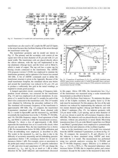
Fig. 13. Transformer 2-% model (left) and transformer geometry (right).<br />
transformers are also used to AC-couple the RF and LO <strong>in</strong>puts<br />
to the mixer because they facilitate bias<strong>in</strong>g of the mixer through<br />
the transformer center tap.<br />
The transformer geometry and its model are shown <strong>in</strong><br />
Fig. 13. The primary and the secondary coils consist of one<br />
square turn with an <strong>in</strong>ner diameter of 20 m and with 2.5 m<br />
metal width. The transformer coils are placed directly above<br />
the silicon substrate, with the top coil implemented <strong>in</strong> the<br />
top alum<strong>in</strong>um (Alucap) layer, and the lower coil <strong>in</strong> Metal 6,<br />
which is made of copper. The top coil has a center tap for<br />
bias<strong>in</strong>g circuits connected to the transformer. The ASITIC<br />
[24] program (version 3.19.00) was employed to simulate the<br />
transformer geometry and to optimize it for lowest loss around<br />
160 <strong>GHz</strong>. A list of ASITIC commands used to def<strong>in</strong>e the<br />
transformer structure is given <strong>in</strong> the Appendix. Because of the<br />
small transformer footpr<strong>in</strong>t, the simulated silicon area below<br />
and around the transformer was reduced to 64 m 64 m<br />
to produce a sufficiently f<strong>in</strong>e grid <strong>in</strong> the metal w<strong>in</strong>d<strong>in</strong>gs, as<br />
required to ensure good accuracy.<br />
A lumped equivalent circuit, consist<strong>in</strong>g of frequency-<strong>in</strong>dependent<br />
circuit elements, was extracted for the transformer<br />
(Fig. 13) and was employed <strong>in</strong> all circuit simulations. It comprises<br />
a 2- model for the coils and 2- models for each of the<br />
short wires connected to the transformer coils. The 2- models<br />
were obta<strong>in</strong>ed by follow<strong>in</strong>g the procedure outl<strong>in</strong>ed <strong>in</strong> [25].<br />
The simulated self-resonance frequency of the transformer is<br />
approximately 400 <strong>GHz</strong>. Fig. 14 compares the transformer<br />
S-parameters simulated with ASITIC, those obta<strong>in</strong>ed with<br />
the 2- model <strong>in</strong> SpectreRF, and the measured and MAG<br />
(essentially the transformer loss) <strong>in</strong> the 1–70-<strong>GHz</strong>, 57–94-<strong>GHz</strong>,<br />
and 116–184-<strong>GHz</strong> frequency ranges. Good agreement of both<br />
and MAG is achieved, with<strong>in</strong> the measurement accuracy.<br />
Although shows a loss of approximately 4 dB, MAG<br />
represents the transformer loss as it is used <strong>in</strong> the circuit, when<br />
all ports are matched. Thus, the true transformer loss is below<br />
2 dB. For measurements below 94 <strong>GHz</strong>, LRM calibration and<br />
T-l<strong>in</strong>e de-embedd<strong>in</strong>g were employed, as described <strong>in</strong> [26].<br />
The scatter <strong>in</strong> the measured and data is due to the<br />
difficulty of accurately measur<strong>in</strong>g and de-embedd<strong>in</strong>g parasitic<br />
capacitances (below 1 fF), resistances (below 0.1 ) and <strong>in</strong>ductances<br />
(below 1 pH). For example, errors or uncerta<strong>in</strong>ty <strong>in</strong><br />
the probe-pad contact resistance of 0.1 , parasitic <strong>in</strong>ductance<br />
of 1 pH, and error <strong>in</strong> pad capacitance of 2 fF, can change the<br />
measured , and by as much as 1 dB <strong>in</strong> either<br />
direction for the small <strong>in</strong>ductors and transformers discussed<br />
Fig. 14. Comparison of transformer ƒ ƒ ƒ and MAG simulated us<strong>in</strong>g<br />
ASITIC (open circles), modeled with 2-% model <strong>in</strong> SpectreRF (l<strong>in</strong>es), and measured<br />
<strong>in</strong> three frequency ranges (dots) us<strong>in</strong>g two VNAs and power <strong>in</strong>sertion loss<br />
measurements beyond 110 <strong>GHz</strong>.<br />
<strong>in</strong> this paper. Above 100 <strong>GHz</strong>, the transmission loss<br />
of the transformer was measured us<strong>in</strong>g a scalar transmission<br />
measurement as described <strong>in</strong> Section V.<br />
2) 50-pH Oscillator Tank Inductor: To m<strong>in</strong>imize the phase<br />
noise of the Colpitts oscillator, the quality factor of the<br />
tank must be maximized. For this purpose, the loss of the tank<br />
<strong>in</strong>ductor was reduced by implement<strong>in</strong>g the <strong>in</strong>ductor coil with<br />
two metals shunted together (Alucap and Metal 6), and with<br />
a Metal 5 underpass (Fig. 15). An <strong>in</strong>ductor geometry with<br />
2.8- m metal width, 2- m spac<strong>in</strong>g, and an <strong>in</strong>ner diameter of<br />
9 m was chosen to push the self-resonance frequency above<br />
400 <strong>GHz</strong>. The <strong>in</strong>ductor coil was placed directly over the silicon<br />
substrate, without any polysilicon or metal shield. Microstrip<br />
transmission l<strong>in</strong>es (3.6- m-wide Metal 6 signal l<strong>in</strong>e over Metal<br />
1 and Metal 2 ground plane) were employed to symmetrically<br />
connect the four tank <strong>in</strong>ductors of the oscillator together.<br />
Just as <strong>in</strong> the transformer case, a 2- model was extracted<br />
from the ASITIC simulated Y-parameters, as shown <strong>in</strong> Fig. 15.<br />
Fig. 16 compares the measured L, R and effective of<br />
the <strong>in</strong>ductor to those simulated us<strong>in</strong>g ASITIC and modeled<br />
with the 2- model. The measurement was performed<br />
us<strong>in</strong>g two network analyzers cover<strong>in</strong>g the 1–70-<strong>GHz</strong> and<br />
the 57–94-<strong>GHz</strong> frequency ranges. Effective is def<strong>in</strong>ed as<br />
. The measured <strong>in</strong>ductance value<br />
<strong>in</strong>creases below 10 <strong>GHz</strong> due to imperfect probes and contact<br />
resistance. Except for the scatter <strong>in</strong> the measured data <strong>in</strong> the


