

165-GHz Transceiver in SiGe Technology - Computer Engineering ...
165-GHz Transceiver in SiGe Technology - Computer Engineering ...
165-GHz Transceiver in SiGe Technology - Computer Engineering ...

Create successful ePaper yourself
Turn your PDF publications into a flip-book with our unique Google optimized e-Paper software.
LASKIN et al.: <strong>165</strong>-GHZ TRANSCEIVER IN SIGE TECHNOLOGY 1095<br />
Fig. 15. Inductor 2-% model (left) and <strong>in</strong>ductor geometry (right).<br />
Fig. 16. Comparison of <strong>in</strong>ductor L, R, and simulated us<strong>in</strong>g ASITIC, modeled<br />
with 2-% model, and measured over two frequency ranges us<strong>in</strong>g two different<br />
VNAs.<br />
57–94-<strong>GHz</strong> range due to the difficulty of measur<strong>in</strong>g resistance<br />
with less than 0.1- accuracy, the agreement between simulations<br />
and measurements is very good.<br />
IV. FABRICATION<br />
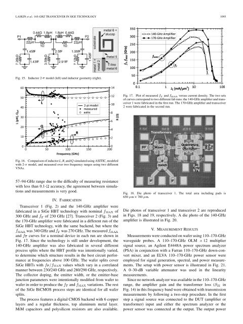
<strong>Transceiver</strong> 1 (Fig. 2) and the 140-<strong>GHz</strong> amplifier were<br />
fabricated <strong>in</strong> a <strong>SiGe</strong> HBT technology with nom<strong>in</strong>al of<br />
300 <strong>GHz</strong> and of 230 <strong>GHz</strong> [27]. <strong>Transceiver</strong> 2 (Fig. 3) and<br />
the 170-<strong>GHz</strong> amplifier were fabricated <strong>in</strong> a different run of the<br />
<strong>SiGe</strong> HBT technology, with the same backend, but where the<br />
was 340 <strong>GHz</strong> and was 270 <strong>GHz</strong>. The measured<br />
and curves for a nom<strong>in</strong>al device <strong>in</strong> each run are shown <strong>in</strong><br />
Fig. 17. S<strong>in</strong>ce the technology is still under development, the<br />
140-<strong>GHz</strong> amplifier was also fabricated <strong>in</strong> several different<br />
process splits where the HBT profile was <strong>in</strong>tentionally varied,<br />
to determ<strong>in</strong>e which structure results <strong>in</strong> the best circuit performance<br />
at frequencies above 100 <strong>GHz</strong>. The wafer splits cover<br />
<strong>SiGe</strong> HBTs with values which vary <strong>in</strong> a correlated<br />
manner between 230/240 <strong>GHz</strong> and 280/290 <strong>GHz</strong>, respectively.<br />
The collector dop<strong>in</strong>g, the emitter width, or the emitter-base<br />
junction parameters were <strong>in</strong>tentionally modified from wafer to<br />
wafer <strong>in</strong> order to produce the and variations. The rest<br />
of the <strong>SiGe</strong> BiCMOS process steps are identical for all wafer<br />
splits.<br />
The process features a digital CMOS backend with 6 copper<br />
layers and a regular thickness, top alum<strong>in</strong>um metal layer.<br />
MiM capacitors and polysilicon resistors are also available.<br />
Fig. 17. Plot of measured � and � versus current density. The two sets<br />
of curves correspond to two different fab runs: the 140-<strong>GHz</strong> amplifier and transceiver<br />
1 were fabricated <strong>in</strong> the first run. The 170-<strong>GHz</strong> amplifier and transceiver<br />
2 were fabricated <strong>in</strong> the second run.<br />
Fig. 18. Die photo of transceiver 1. The total area <strong>in</strong>clud<strong>in</strong>g pads is<br />
650 "m2 700 "m.<br />
Die photos of transceiver 1 and transceiver 2 are reproduced<br />
<strong>in</strong> Figs. 18 and 19, respectively. A die photo of the 140-<strong>GHz</strong><br />
amplifier is illustrated <strong>in</strong> Fig. 20.<br />
V. MEASUREMENT RESULTS<br />
Measurements were conducted on wafer us<strong>in</strong>g 110–170-<strong>GHz</strong><br />
waveguide probes. A 110–170-<strong>GHz</strong> OLM 12 multiplier<br />
signal source, an Agilent E4448A power spectrum analyzer<br />
(PSA) <strong>in</strong> conjunction with a Farran 110–170-<strong>GHz</strong> down-convert<br />
mixer, and an ELVA 110–170-<strong>GHz</strong> power sensor were<br />
employed for signal generation, spectral, and power measurements.<br />
The setup with power sensor is illustrated <strong>in</strong> Fig. 21.<br />
A 0–30-dB variable attenuator was used <strong>in</strong> the l<strong>in</strong>earity<br />
measurements.<br />
S<strong>in</strong>ce no network analyzer was available <strong>in</strong> the 110–170-<strong>GHz</strong><br />
range, the amplifier ga<strong>in</strong> and the transformer loss ( <strong>in</strong><br />
Fig. 14) <strong>in</strong> this frequency band were obta<strong>in</strong>ed with transmission<br />
measurements by follow<strong>in</strong>g a two-step procedure. In the first<br />
step a signal source was connected to the DUT (amplifier or<br />
transformer) <strong>in</strong>put and either the spectrum analyzer or the<br />
power sensor was connected at the output. The output power


