

165-GHz Transceiver in SiGe Technology - Computer Engineering ...
165-GHz Transceiver in SiGe Technology - Computer Engineering ...
165-GHz Transceiver in SiGe Technology - Computer Engineering ...

You also want an ePaper? Increase the reach of your titles
YUMPU automatically turns print PDFs into web optimized ePapers that Google loves.
LASKIN et al.: <strong>165</strong>-GHZ TRANSCEIVER IN SIGE TECHNOLOGY 1093<br />
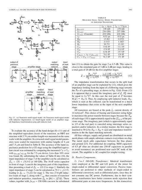
Fig. 12. (a) Transistor small-signal model. (b) Transistor small-signal model<br />
with <strong>in</strong>ductive degeneration. (c) Small-signal model of an amplifier stage.<br />
(d) Impedance transformation us<strong>in</strong>g split <strong>in</strong>ductor load.<br />
To evaluate the accuracy of the hand-design (8)–(11) and of<br />
the simplified equivalent circuit of the transistor, an HBT test<br />
structure with 5.74 m emitter length was measured on the same<br />
wafer with the amplifier. Its extracted small signal model parameters<br />
were scaled for transistors with emitter lengths of 4 m<br />
and 7.5 m and listed <strong>in</strong> Table II. The accuracy of the <strong>in</strong>put capacitance<br />
prediction for a CE stage us<strong>in</strong>g the simplified equivalent<br />
circuit was estimated by compar<strong>in</strong>g the measured<br />
with for the 7.5- m device. Less than 10% error<br />
was found. By substitut<strong>in</strong>g the values of Table II <strong>in</strong>to (10), the<br />
<strong>in</strong>put impedance of stage 3 of the amplifier can be calculated as<br />
at 140 <strong>GHz</strong>. The 16-fF series capacitor<br />
<strong>in</strong> front of stage 3 cancels the imag<strong>in</strong>ary part of this impedance,<br />
thus present<strong>in</strong>g a load of to stage 2. Similarly the<br />
<strong>in</strong>put impedance of stage 2 can be calculated as ,<br />
lead<strong>in</strong>g to for stage 2. The two 27.6-pH <strong>in</strong>ductive<br />
loads of stage 2, along with that consists of transistor<br />
and <strong>in</strong>ductor parasitics, transform to . These<br />
values, together with <strong>GHz</strong> can now be substituted<br />
TABLE II<br />
MEASURED SMALL SIGNAL MODEL PARAMETERS<br />
OF AMPLIFIER TRANSISTORS<br />
<strong>in</strong>to (11) to obta<strong>in</strong> the ga<strong>in</strong> for stage 2 as 4.3 dB. This value is<br />
close to the simulated ga<strong>in</strong> of 3 dB to 4 dB per stage, lead<strong>in</strong>g to<br />
a total ga<strong>in</strong> of 20 dB for the five amplifier stages<br />
(12)<br />
The impedance transformation that occurs <strong>in</strong> the split load<br />
of an amplifier stage can be expla<strong>in</strong>ed by (12), which gives the<br />
impedance look<strong>in</strong>g from the <strong>in</strong>put of a follow<strong>in</strong>g stage towards<br />
the of a preced<strong>in</strong>g stage, as shown <strong>in</strong> Fig. 12(d). From (12)<br />
it is apparent that to cancel the imag<strong>in</strong>ary part of must<br />
be equal to . In this case the real part of becomes<br />
. Thus, by employ<strong>in</strong>g split <strong>in</strong>ductor loads, ,<br />
which is seen at the collector, can be transformed to a much<br />
lower impedance that exists at the <strong>in</strong>put of the next amplifier<br />
stage.<br />
All transistors are biased at the peak- current density of<br />
14 mA/ m . This choice of bias<strong>in</strong>g and transistor siz<strong>in</strong>g helps<br />
to maximize the power transfer between stages because the<br />
of each stage (10) is approximately equal to the of the previous<br />
stage. The imag<strong>in</strong>ary part (which is approximately equal<br />
to 1/3 of the real part) is canceled us<strong>in</strong>g <strong>in</strong>terstage series capacitors<br />
and/or <strong>in</strong>ductors. In a similar manner, the first stage is<br />
matched to 50 by and impedance transformation<br />
<strong>in</strong> the the <strong>in</strong>put match<strong>in</strong>g network.<br />
All bias voltages, supply and ground are distributed on metal<br />
mesh planes with ample substrate contacts everywhere on chip.<br />
The metal mesh adds capacitance between the bias planes<br />
and ground [23]. For additional de-coupl<strong>in</strong>g, MiM capacitors<br />
of 0.5 pF (that are divided <strong>in</strong>to 250-fF capacitors <strong>in</strong> parallel<br />
to avoid resonance) are positioned near each DC node of the<br />
circuit. The amplifier is AC-coupled for simpler test<strong>in</strong>g.<br />
D. Passive Components<br />
1) 1-to-1 160-<strong>GHz</strong> Transformer: Identical transformers<br />
were employed at the RF and LO ports of the mixer for<br />
s<strong>in</strong>gle-ended to differential signal conversion. Passive transformers<br />
are preferred to other methods of s<strong>in</strong>gle-ended to<br />
differential conversion, such as differential pairs, s<strong>in</strong>ce they do<br />
not consume any DC power. Furthermore, due to their symmetry,<br />
transformers have better common mode rejection than<br />
differential pairs at mm-wave frequencies. In this transceiver,


