

165-GHz Transceiver in SiGe Technology - Computer Engineering ...
165-GHz Transceiver in SiGe Technology - Computer Engineering ...
165-GHz Transceiver in SiGe Technology - Computer Engineering ...

Create successful ePaper yourself
Turn your PDF publications into a flip-book with our unique Google optimized e-Paper software.
1092 IEEE JOURNAL OF SOLID-STATE CIRCUITS, VOL. 43, NO. 5, MAY 2008<br />
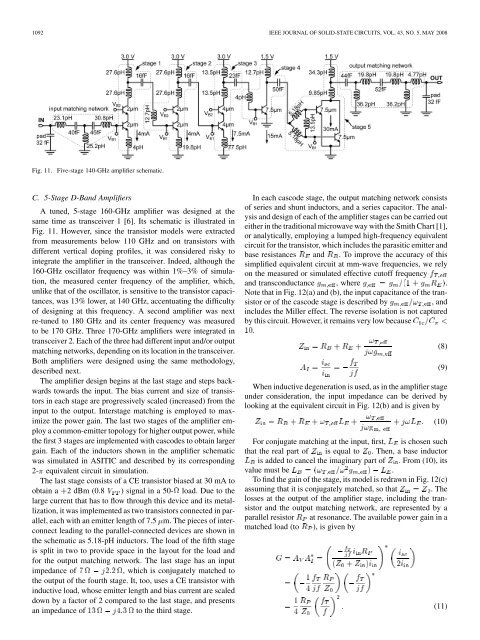
Fig. 11. Five-stage 140-<strong>GHz</strong> amplifier schematic.<br />
C. 5-Stage D-Band Amplifiers<br />
A tuned, 5-stage 160-<strong>GHz</strong> amplifier was designed at the<br />
same time as transceiver 1 [6]. Its schematic is illustrated <strong>in</strong><br />
Fig. 11. However, s<strong>in</strong>ce the transistor models were extracted<br />
from measurements below 110 <strong>GHz</strong> and on transistors with<br />
different vertical dop<strong>in</strong>g profiles, it was considered risky to<br />
<strong>in</strong>tegrate the amplifier <strong>in</strong> the transceiver. Indeed, although the<br />
160-<strong>GHz</strong> oscillator frequency was with<strong>in</strong> 1%–3% of simulation,<br />
the measured center frequency of the amplifier, which,<br />
unlike that of the oscillator, is sensitive to the transistor capacitances,<br />
was 13% lower, at 140 <strong>GHz</strong>, accentuat<strong>in</strong>g the difficulty<br />
of design<strong>in</strong>g at this frequency. A second amplifier was next<br />
re-tuned to 180 <strong>GHz</strong> and its center frequency was measured<br />
to be 170 <strong>GHz</strong>. Three 170-<strong>GHz</strong> amplifiers were <strong>in</strong>tegrated <strong>in</strong><br />
transceiver 2. Each of the three had different <strong>in</strong>put and/or output<br />
match<strong>in</strong>g networks, depend<strong>in</strong>g on its location <strong>in</strong> the transceiver.<br />
Both amplifiers were designed us<strong>in</strong>g the same methodology,<br />
described next.<br />
The amplifier design beg<strong>in</strong>s at the last stage and steps backwards<br />
towards the <strong>in</strong>put. The bias current and size of transistors<br />
<strong>in</strong> each stage are progressively scaled (<strong>in</strong>creased) from the<br />
<strong>in</strong>put to the output. Interstage match<strong>in</strong>g is employed to maximize<br />
the power ga<strong>in</strong>. The last two stages of the amplifier employ<br />
a common-emitter topology for higher output power, while<br />
the first 3 stages are implemented with cascodes to obta<strong>in</strong> larger<br />
ga<strong>in</strong>. Each of the <strong>in</strong>ductors shown <strong>in</strong> the amplifier schematic<br />
was simulated <strong>in</strong> ASITIC and described by its correspond<strong>in</strong>g<br />
2- equivalent circuit <strong>in</strong> simulation.<br />
The last stage consists of a CE transistor biased at 30 mA to<br />
obta<strong>in</strong> a 2 dBm (0.8 ) signal <strong>in</strong> a 50- load. Due to the<br />
large current that has to flow through this device and its metallization,<br />
it was implemented as two transistors connected <strong>in</strong> parallel,<br />
each with an emitter length of 7.5 m. The pieces of <strong>in</strong>terconnect<br />
lead<strong>in</strong>g to the parallel-connected devices are shown <strong>in</strong><br />
the schematic as 5.18-pH <strong>in</strong>ductors. The load of the fifth stage<br />
is split <strong>in</strong> two to provide space <strong>in</strong> the layout for the load and<br />
for the output match<strong>in</strong>g network. The last stage has an <strong>in</strong>put<br />
impedance of , which is conjugately matched to<br />
the output of the fourth stage. It, too, uses a CE transistor with<br />
<strong>in</strong>ductive load, whose emitter length and bias current are scaled<br />
down by a factor of 2 compared to the last stage, and presents<br />
an impedance of to the third stage.<br />
In each cascode stage, the output match<strong>in</strong>g network consists<br />
of series and shunt <strong>in</strong>ductors, and a series capacitor. The analysis<br />
and design of each of the amplifier stages can be carried out<br />
either <strong>in</strong> the traditional microwave way with the Smith Chart [1],<br />
or analytically, employ<strong>in</strong>g a lumped high-frequency equivalent<br />
circuit for the transistor, which <strong>in</strong>cludes the parasitic emitter and<br />
base resistances and . To improve the accuracy of this<br />
simplified equivalent circuit at mm-wave frequencies, we rely<br />
on the measured or simulated effective cutoff frequency<br />
and transconductance , where .<br />
Note that <strong>in</strong> Fig. 12(a) and (b), the <strong>in</strong>put capacitance of the transistor<br />
or of the cascode stage is described by , and<br />
<strong>in</strong>cludes the Miller effect. The reverse isolation is not captured<br />
by this circuit. However, it rema<strong>in</strong>s very low because<br />
.<br />
When <strong>in</strong>ductive degeneration is used, as <strong>in</strong> the amplifier stage<br />
under consideration, the <strong>in</strong>put impedance can be derived by<br />
look<strong>in</strong>g at the equivalent circuit <strong>in</strong> Fig. 12(b) and is given by<br />
(8)<br />
(9)<br />
(10)<br />
For conjugate match<strong>in</strong>g at the <strong>in</strong>put, first, is chosen such<br />
that the real part of is equal to . Then, a base <strong>in</strong>ductor<br />
is added to cancel the imag<strong>in</strong>ary part of . From (10), its<br />
value must be .<br />
To f<strong>in</strong>d the ga<strong>in</strong> of the stage, its model is redrawn <strong>in</strong> Fig. 12(c)<br />
assum<strong>in</strong>g that it is conjugately matched, so that . The<br />
losses at the output of the amplifier stage, <strong>in</strong>clud<strong>in</strong>g the transistor<br />
and the output match<strong>in</strong>g network, are represented by a<br />
parallel resistor at resonance. The available power ga<strong>in</strong> <strong>in</strong> a<br />
matched load (to ), is given by<br />
(11)


