

165-GHz Transceiver in SiGe Technology - Computer Engineering ...
165-GHz Transceiver in SiGe Technology - Computer Engineering ...
165-GHz Transceiver in SiGe Technology - Computer Engineering ...

Create successful ePaper yourself
Turn your PDF publications into a flip-book with our unique Google optimized e-Paper software.
1096 IEEE JOURNAL OF SOLID-STATE CIRCUITS, VOL. 43, NO. 5, MAY 2008<br />
Fig. 19. Die photo of transceiver 2 with <strong>in</strong>tegrated amplifiers and static frequency<br />
divider. The total area <strong>in</strong>clud<strong>in</strong>g pads is 840 "m21365 "m.<br />
Fig. 20. Die photo of the 140-<strong>GHz</strong>. The active circuit area is 200 "m2<br />
400 "m.<br />
Fig. 21. On-wafer 160-<strong>GHz</strong> test setup for transmitter output power measurements<br />
show<strong>in</strong>g the signal source on the left, applied at the receiver <strong>in</strong>put<br />
through 110–170-<strong>GHz</strong> waveguide probes. The 110–170-<strong>GHz</strong> power sensor is<br />
at the right. The IF output is collected at the bottom with differential probes.<br />
was recorded at each frequency. In the second step, the output<br />
power was recorded aga<strong>in</strong>, after replac<strong>in</strong>g the DUT by a “thru”<br />
located on a standard 110-<strong>GHz</strong> Cascade Microtech calibration<br />
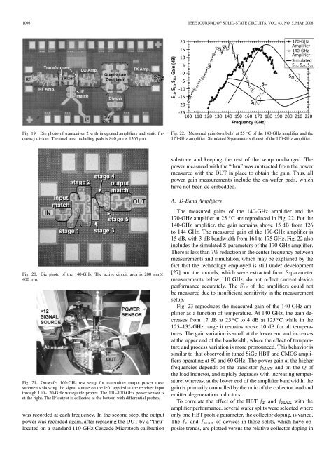
Fig. 22. Measured ga<strong>in</strong> (symbols) at 25 C of the 140-<strong>GHz</strong> amplifier and the<br />
170-<strong>GHz</strong> amplifier. Simulated S-parameters (l<strong>in</strong>es) of the 170-<strong>GHz</strong> amplifier.<br />
substrate and keep<strong>in</strong>g the rest of the setup unchanged. The<br />
power measured with the “thru” was subtracted from the power<br />
measured with the DUT <strong>in</strong> place to obta<strong>in</strong> the ga<strong>in</strong>. Thus, all<br />
power ga<strong>in</strong> measurements <strong>in</strong>clude the on-wafer pads, which<br />
have not been de-embedded.<br />
A. D-Band Amplifiers<br />
The measured ga<strong>in</strong>s of the 140-<strong>GHz</strong> amplifier and the<br />
170-<strong>GHz</strong> amplifier at 25 C are reproduced <strong>in</strong> Fig. 22. For the<br />
140-<strong>GHz</strong> amplifier, the ga<strong>in</strong> rema<strong>in</strong>s above 15 dB from 126<br />
to 144 <strong>GHz</strong>. The measured ga<strong>in</strong> of the 170-<strong>GHz</strong> amplifier is<br />
15 dB, with 3-dB bandwidth from 164 to 175 <strong>GHz</strong>. Fig. 22 also<br />
<strong>in</strong>cludes the simulated S-parameters of the 170-<strong>GHz</strong> amplifier.<br />
There is less than 7% reduction <strong>in</strong> the center frequency between<br />
measurements and simulation, which may be expla<strong>in</strong>ed by the<br />
fact that the technology employed is still under development<br />
[27] and the models, which were extracted from S-parameter<br />
measurements below 110 <strong>GHz</strong>, do not reflect current device<br />
performance accurately. The of the amplifiers could not<br />
be measured due to <strong>in</strong>sufficient sensitivity <strong>in</strong> the measurement<br />
setup.<br />
Fig. 23 reproduces the measured ga<strong>in</strong> of the 140-<strong>GHz</strong> amplifier<br />
as a function of temperature. At 140 <strong>GHz</strong>, the ga<strong>in</strong> decreases<br />
from 17 dB at 25 C to 4 dB at 125 C while <strong>in</strong> the<br />
125–135-<strong>GHz</strong> range it rema<strong>in</strong>s above 10 dB for all temperatures.<br />
The ga<strong>in</strong> variation is small at the lower end and <strong>in</strong>creases<br />
at the upper end of the bandwidth, where the effect of temperature<br />
and process variation is more pronounced. This behavior is<br />
similar to that observed <strong>in</strong> tuned <strong>SiGe</strong> HBT and CMOS amplifiers<br />
operat<strong>in</strong>g at 80 and 60 <strong>GHz</strong>. The power ga<strong>in</strong> at the higher<br />
frequencies depends on the transistor and on the of<br />
the load <strong>in</strong>ductor, and rapidly degrades with <strong>in</strong>creas<strong>in</strong>g temperature,<br />
whereas, at the lower end of the amplifier bandwidth, the<br />
ga<strong>in</strong> is primarily controlled by the ratio of the collector load and<br />
emitter degeneration <strong>in</strong>ductors.<br />
To correlate the effect of the HBT and with the<br />
amplifier performance, several wafer splits were selected where<br />
only one HBT profile parameter, the collector dop<strong>in</strong>g, is varied.<br />
The and of devices <strong>in</strong> those splits, which have opposite<br />
trends, are plotted versus the relative collector dop<strong>in</strong>g <strong>in</strong>


