

Xcell Journal Issue 78: Charge to Market with Xilinx 7 Series ...
Xcell Journal Issue 78: Charge to Market with Xilinx 7 Series ...
Xcell Journal Issue 78: Charge to Market with Xilinx 7 Series ...

You also want an ePaper? Increase the reach of your titles
YUMPU automatically turns print PDFs into web optimized ePapers that Google loves.
XCELLENCE IN PROTOTYPING<br />
3.3<br />
GPIO<br />
V5a<br />
47 38<br />
B5<br />
48 37<br />
B3<br />
42 44<br />
119<br />
10 LS<br />
V4a<br />
V4a V5a<br />
43 45<br />
3.3<br />
GPIO<br />
V5a<br />
31 33<br />
B1<br />
30 32<br />
V3a<br />
47 30<br />
A5<br />
48 37<br />
V2a<br />
43 45<br />
A3<br />
42 44<br />
A1<br />
30 32<br />
119<br />
119<br />
119<br />
119<br />
10 LS<br />
V4a V5a<br />
V1a<br />
31 33<br />
119<br />
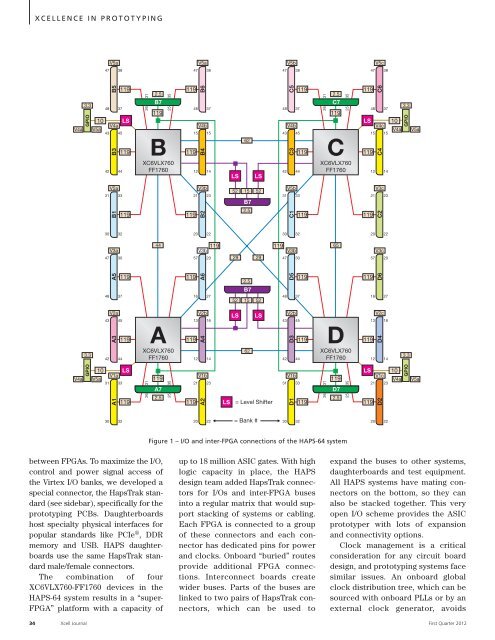
between FPGAs. To maximize the I/O,<br />
control and power signal access of<br />
the Virtex I/O banks, we developed a<br />
special connec<strong>to</strong>r, the HapsTrak standard<br />
(see sidebar), specifically for the<br />
pro<strong>to</strong>typing PCBs. Daughterboards<br />
host specialty physical interfaces for<br />
popular standards like PCIe ® , DDR<br />
memory and USB. HAPS daughterboards<br />
use the same HapsTrak standard<br />
male/female connec<strong>to</strong>rs.<br />
The combination of four<br />
XC6VLX760-FF1760 devices in the<br />
HAPS-64 system results in a “super-<br />
FPGA” platform <strong>with</strong> a capacity of<br />
31<br />
26<br />
2.5<br />
B7<br />
119<br />
35<br />
25<br />
B<br />
XC6VLX760<br />
FF1760<br />
31<br />
26<br />
44<br />
A<br />
XC6VLX760<br />
FF1760<br />
119<br />
A7<br />
2.5<br />
35<br />
25<br />
119<br />
119<br />
119<br />
119<br />
119<br />
119<br />
V5a<br />
47 38<br />
B6<br />
48 37<br />
V4b<br />
15 15<br />
B4<br />
12 14<br />
V3b<br />
21 23<br />
B2<br />
20 22<br />
A6<br />
16 27<br />
V2b<br />
13 16<br />
A4<br />
12 14<br />
V1b<br />
21 23<br />
A2<br />
20 22<br />
up <strong>to</strong> 18 million ASIC gates. With high<br />
logic capacity in place, the HAPS<br />
design team added HapsTrak connec<strong>to</strong>rs<br />
for I/Os and inter-FPGA buses<br />
in<strong>to</strong> a regular matrix that would support<br />
stacking of systems or cabling.<br />
Each FPGA is connected <strong>to</strong> a group<br />
of these connec<strong>to</strong>rs and each connec<strong>to</strong>r<br />
has dedicated pins for power<br />
and clocks. Onboard “buried” routes<br />
provide additional FPGA connections.<br />
Interconnect boards create<br />
wider buses. Parts of the buses are<br />
linked <strong>to</strong> two pairs of HapsTrak connec<strong>to</strong>rs,<br />
which can be used <strong>to</strong><br />
expand the buses <strong>to</strong> other systems,<br />
daughterboards and test equipment.<br />
All HAPS systems have mating connec<strong>to</strong>rs<br />
on the bot<strong>to</strong>m, so they can<br />
also be stacked <strong>to</strong>gether. This very<br />
open I/O scheme provides the ASIC<br />
pro<strong>to</strong>typer <strong>with</strong> lots of expansion<br />
and connectivity options.<br />
Clock management is a critical<br />
consideration for any circuit board<br />
design, and pro<strong>to</strong>typing systems face<br />
similar issues. An onboard global<br />
clock distribution tree, which can be<br />
sourced <strong>with</strong> onboard PLLs or by an<br />
external clock genera<strong>to</strong>r, avoids<br />
34 <strong>Xcell</strong> <strong>Journal</strong> First Quarter 2012<br />
V5b<br />
47 38<br />
C5<br />
48 37<br />
V4b<br />
43 45<br />
C3<br />
42 44<br />
V5b<br />
31 33<br />
C1<br />
30 32<br />
119<br />
V3b<br />
119<br />
V3b<br />
57 20 29 29<br />
47 30<br />
LS<br />
62<br />
LS LS<br />
52 15<br />
B7<br />
2.5<br />
2.5<br />
B7<br />
62<br />
52<br />
52 15 52<br />
LS LS<br />
= Level Shifter<br />
= Bank #<br />
D5<br />
48 37<br />
V2b<br />
43 45<br />
D3<br />
42 44<br />
V1b<br />
31 33<br />
D1<br />
30 32<br />
119<br />
119<br />
119<br />
119<br />
119<br />
119<br />
31<br />
26<br />
2.5<br />
C7<br />
119<br />
35<br />
25<br />
C<br />
XC6VLX760<br />
FF1760<br />
31<br />
26<br />
65<br />
D<br />
XC6VLX760<br />
FF1760<br />
Figure 1 – I/O and inter-FPGA connections of the HAPS-64 system<br />
119<br />
D7<br />
2.5<br />
35<br />
25<br />
119<br />
LS<br />
119<br />
119<br />
119<br />
119<br />
LS<br />
119<br />
V5c<br />
47 38<br />
C6<br />
48 37<br />
V4c<br />
15 15<br />
C4<br />
12 14<br />
V3c<br />
21 23<br />
C2<br />
20 22<br />
V3c<br />
57 20<br />
D6<br />
16 27<br />
V2c<br />
13 16<br />
D4<br />
12 14<br />
V1c<br />
21 23<br />
D2<br />
20 22<br />
10<br />
10<br />
3.3<br />
GPIO<br />
V4a V5a<br />
3.3<br />
GPIO<br />
V4a V5a


