BLOCKING READER: DESIGN AND IMPLEMENTATION OF A ...
BLOCKING READER: DESIGN AND IMPLEMENTATION OF A ...
BLOCKING READER: DESIGN AND IMPLEMENTATION OF A ...
You also want an ePaper? Increase the reach of your titles
YUMPU automatically turns print PDFs into web optimized ePapers that Google loves.
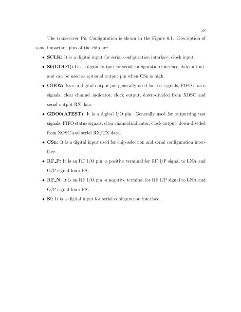
The transceiver Pin Configuration is shown in the Figure 6.1. Description of<br />
some important pins of the chip are<br />
• SCLK: It is a digital input for serial configuration interface, clock input.<br />
• S0(GDO1): It is a digital output for serial configuration interface, data output.<br />
and can be used as optional output pin when CSn is high.<br />
• GDO2: Its is a digital output pin generally used for test signals, FIFO status<br />
signals, clear channel indicator, clock output, down-divided from XOSC and<br />
serial output RX data<br />
• GDO0(ATEST): It is a digital I/O pin. Generally used for outputting test<br />
signals, FIFO status signals, clear channel indicator, clock output, down-divided<br />
from XOSC and serial RX/TX data.<br />
• CSn: It is a digital input used for chip selection and serial configuration inter-<br />
face.<br />
• RF P: It is an RF I/O pin, a positive terminal for RF I/P signal to LNA and<br />
O/P signal from PA.<br />
• RF N: It is an RF I/O pin, a negative terminal for RF I/P signal to LNA and<br />
O/P signal from PA.<br />
• SI: It is a digital input for serial configuration interface.<br />
58


