Thermal properties in mesoscopics: physics and ... - ResearchGate
Thermal properties in mesoscopics: physics and ... - ResearchGate
Thermal properties in mesoscopics: physics and ... - ResearchGate

Create successful ePaper yourself
Turn your PDF publications into a flip-book with our unique Google optimized e-Paper software.
optimal bias voltage (Vopt), Vopt ≈ (∆ − 0.66kBTe,N )/e,<br />
as well as for the maximum cool<strong>in</strong>g power at Vopt,<br />
˙Qopt ≈ ∆2<br />
e2 kBTe,N<br />
[0.59( RT ∆<br />
)3/2<br />
<br />
2πkBTe,S<br />
− ∆ exp(− ∆<br />
kBTe,S )].<br />
(78)<br />
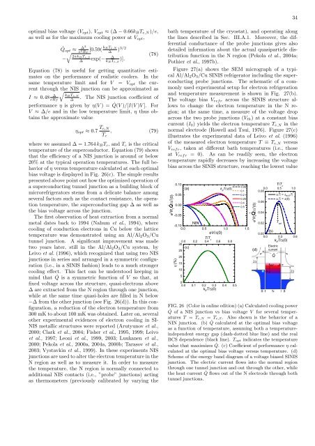
Equation (78) is useful for gett<strong>in</strong>g quantitative estimates<br />
on the performance of realistic coolers. In the<br />
same temperature limit <strong>and</strong> for V = Vopt the cur-<br />
rent through the NIS junction can be approximated as<br />
I ≈ 0.48 ∆<br />
eRT<br />
<br />
kBTe,N<br />
∆ . The NIS junction coefficient of<br />
performance η is given by η(V ) = ˙ Q(V )/[I(V )V ]. For<br />
V ≈ ∆/e <strong>and</strong> <strong>in</strong> the low temperature limit, η thus obta<strong>in</strong>s<br />
the approximate value<br />
ηopt ≈ 0.7 Te,N<br />
, (79)<br />
where we assumed ∆ = 1.764 kBTc, <strong>and</strong> Tc is the critical<br />
temperature of the superconductor. Equation (79) shows<br />
that the efficiency of a NIS junction is around or below<br />
20% at the typical operation temperatures. The full behavior<br />
of η versus temperature calculated at each optimal<br />
bias voltage is displayed <strong>in</strong> Fig. 26(c). The simple results<br />
presented above po<strong>in</strong>t out how the optimized operation of<br />
a superconduct<strong>in</strong>g tunnel junction as a build<strong>in</strong>g block of<br />
microrefrigerators stems from a delicate balance among<br />
several factors such as the contact resistance, the operation<br />
temperature, the superconduct<strong>in</strong>g gap ∆ as well as<br />
the bias voltage across the junction.<br />
The first observation of heat extraction from a normal<br />
metal dates back to 1994 (Nahum et al., 1994), where<br />
cool<strong>in</strong>g of conduction electrons <strong>in</strong> Cu below the lattice<br />
temperature was demonstrated us<strong>in</strong>g an Al/Al2O3/Cu<br />
tunnel junction. A significant improvement was made<br />
two years later, still <strong>in</strong> the Al/Al2O3/Cu system, by<br />
Leivo et al. (1996), which recognized that us<strong>in</strong>g two NIS<br />
junctions <strong>in</strong> series <strong>and</strong> arranged <strong>in</strong> a symmetric configuration<br />
(i.e., <strong>in</strong> a SINIS fashion) leads to a much stronger<br />
cool<strong>in</strong>g effect. This fact can be understood keep<strong>in</strong>g <strong>in</strong><br />
m<strong>in</strong>d that ˙ Q is a symmetric function of V so that, at<br />
fixed voltage across the structure, quasi-electrons above<br />
∆ are extracted from the N region through one junction,<br />
while at the same time quasi-holes are filled <strong>in</strong> N below<br />
−∆ from the other junction (see Fig. 26(d)). In this configuration,<br />
a reduction of the electron temperature from<br />
300 mK to about 100 mK was obta<strong>in</strong>ed. Later on, several<br />
other experimental evidences of electron cool<strong>in</strong>g <strong>in</strong> SI-<br />
NIS metallic structures were reported (Arutyunov et al.,<br />
2000; Clark et al., 2004; Fisher et al., 1995, 1999; Leivo<br />
et al., 1997; Leoni et al., 1999, 2003; Luukanen et al.,<br />
2000; Pekola et al., 2000a, 2004a, 2000b; Tarasov et al.,<br />
2003; Vystavk<strong>in</strong> et al., 1999). In these experiments NIS<br />
junctions are used to alter the electron temperature <strong>in</strong> the<br />
N region as well as to measure it. In order to measure<br />
the temperature, the N region is normally connected to<br />
additional NIS contacts (i.e., ”probe” junctions) act<strong>in</strong>g<br />
as thermometers (previously calibrated by vary<strong>in</strong>g the<br />
Tc<br />
34<br />
bath temperature of the cryostat), <strong>and</strong> operat<strong>in</strong>g along<br />
the l<strong>in</strong>es described <strong>in</strong> Sec. III.A.1. Moreover, the differential<br />
conductance of the probe junctions gives also<br />
detailed <strong>in</strong>formation about the actual quasiparticle distribution<br />
function <strong>in</strong> the N region (Pekola et al., 2004a;<br />
Pothier et al., 1997b).<br />
Figure 27(a) shows the SEM micrograph of a typical<br />
Al/Al2O3/Cu SINIS refrigerator <strong>in</strong>clud<strong>in</strong>g the superconduct<strong>in</strong>g<br />
probe junctions. The schematic of a commonly<br />
used experimental setup for electron refrigeration<br />
<strong>and</strong> temperature measurement is shown <strong>in</strong> Fig. 27(b).<br />
The voltage bias Vrefr across the SINIS structure allows<br />
to change the electron temperature <strong>in</strong> the N region;<br />
at the same time, a measure of the voltage drop<br />
across the two probe junctions (Vth) at a constant bias<br />
current (I0) yields the electron temperature Te,N <strong>in</strong> the<br />
normal electrode (Rowell <strong>and</strong> Tsui, 1976). Figure 27(c)<br />
illustrates the experimental data of Leivo et al. (1996)<br />
of the measured electron temperature T ≡ Te,N versus<br />
Vrefr, taken at different bath temperatures (i.e., those<br />
at Vrefr = 0). As can be readily seen, the electron<br />
temperature rapidly decreases by <strong>in</strong>creas<strong>in</strong>g the voltage<br />
bias across the SINIS structure, reach<strong>in</strong>g the lowest value<br />
e 2 R T /Δ 2 (0)<br />
Q&Q&<br />
-0.05<br />
η (%)<br />
0.10<br />
0.05<br />
0.00<br />
15<br />
10<br />
5<br />
(a)<br />
k B T/Δ(0)<br />
0<br />
0.0 0.1 0.2 0.3 0.4 0.5<br />
kBT/Δ(0) 0.05<br />
0.1<br />
0.2<br />
0.25<br />
0.4<br />
0.5<br />
e 2 R T /Δ 2 (0)<br />
Q&Q &<br />
T/Tc 0.0<br />
0.08<br />
0.5 1.0<br />
0.06<br />
0.04<br />
Δ(T) = Δ BCS (T)<br />
Δ(T) = Δ(0)<br />
NIN<br />
0.02<br />
-0.10<br />
0.0 0.5 1.0 1.5<br />
eV/Δ(0)<br />
(b)<br />
0.00<br />
T/T<br />
0.0 0.3 0.6<br />
c<br />
0.0 0.2 0.4 0.6 0.8<br />
kBT/Δ(0) 30<br />
Electric<br />
(c)<br />
25<br />
current<br />
20<br />
Q •<br />
(d)<br />
FIG. 26 (Color <strong>in</strong> onl<strong>in</strong>e edition) (a) Calculated cool<strong>in</strong>g power<br />
˙Q of a NIS junction vs bias voltage V for several temperatures<br />
T = Te,N = Te,S. Also shown is the behavior of a<br />
NIN junction. (b) ˙ Q calculated at the optimal bias voltage<br />
as a function of temperature, assum<strong>in</strong>g both a temperature<strong>in</strong>dependent<br />
energy gap (dash-dotted blue l<strong>in</strong>e) <strong>and</strong> the real<br />
BCS dependence (black l<strong>in</strong>e). Topt <strong>in</strong>dicates the temperature<br />
value that maximizes ˙ Q. (c) Coefficient of performance η calculated<br />
at the optimal bias voltage versus temperature. (d)<br />
Scheme of the energy b<strong>and</strong> diagram of a voltage biased SINIS<br />
junction. The electric current flows <strong>in</strong>to the normal region<br />
through one tunnel junction <strong>and</strong> out through the other, while<br />
the heat current ˙ Q flows out of the N electrode through both<br />
tunnel junctions.<br />
T opt